EP1324441A2 - Optical element module - Google Patents
Optical element module Download PDFInfo
- Publication number
- EP1324441A2 EP1324441A2 EP02256083A EP02256083A EP1324441A2 EP 1324441 A2 EP1324441 A2 EP 1324441A2 EP 02256083 A EP02256083 A EP 02256083A EP 02256083 A EP02256083 A EP 02256083A EP 1324441 A2 EP1324441 A2 EP 1324441A2
- Authority
- EP
- European Patent Office
- Prior art keywords
- light emitting
- emitting element
- connecting portion
- coil
- optical element
- Prior art date
- Legal status (The legal status is an assumption and is not a legal conclusion. Google has not performed a legal analysis and makes no representation as to the accuracy of the status listed.)
- Granted
Links
Images









Classifications
-
- G—PHYSICS
- G02—OPTICS
- G02B—OPTICAL ELEMENTS, SYSTEMS OR APPARATUS
- G02B6/00—Light guides; Structural details of arrangements comprising light guides and other optical elements, e.g. couplings
- G02B6/24—Coupling light guides
- G02B6/42—Coupling light guides with opto-electronic elements
- G02B6/4201—Packages, e.g. shape, construction, internal or external details
-
- G—PHYSICS
- G02—OPTICS
- G02B—OPTICAL ELEMENTS, SYSTEMS OR APPARATUS
- G02B6/00—Light guides; Structural details of arrangements comprising light guides and other optical elements, e.g. couplings
- G02B6/24—Coupling light guides
- G02B6/42—Coupling light guides with opto-electronic elements
- G02B6/4201—Packages, e.g. shape, construction, internal or external details
- G02B6/4274—Electrical aspects
-
- G—PHYSICS
- G02—OPTICS
- G02B—OPTICAL ELEMENTS, SYSTEMS OR APPARATUS
- G02B6/00—Light guides; Structural details of arrangements comprising light guides and other optical elements, e.g. couplings
- G02B6/24—Coupling light guides
- G02B6/42—Coupling light guides with opto-electronic elements
- G02B6/4201—Packages, e.g. shape, construction, internal or external details
- G02B6/4274—Electrical aspects
- G02B6/4279—Radio frequency signal propagation aspects of the electrical connection, high frequency adaptations
-
- H—ELECTRICITY
- H01—ELECTRIC ELEMENTS
- H01S—DEVICES USING THE PROCESS OF LIGHT AMPLIFICATION BY STIMULATED EMISSION OF RADIATION [LASER] TO AMPLIFY OR GENERATE LIGHT; DEVICES USING STIMULATED EMISSION OF ELECTROMAGNETIC RADIATION IN WAVE RANGES OTHER THAN OPTICAL
- H01S5/00—Semiconductor lasers
- H01S5/02—Structural details or components not essential to laser action
- H01S5/022—Mountings; Housings
- H01S5/02208—Mountings; Housings characterised by the shape of the housings
- H01S5/02216—Butterfly-type, i.e. with electrode pins extending horizontally from the housings
-
- H—ELECTRICITY
- H01—ELECTRIC ELEMENTS
- H01S—DEVICES USING THE PROCESS OF LIGHT AMPLIFICATION BY STIMULATED EMISSION OF RADIATION [LASER] TO AMPLIFY OR GENERATE LIGHT; DEVICES USING STIMULATED EMISSION OF ELECTROMAGNETIC RADIATION IN WAVE RANGES OTHER THAN OPTICAL
- H01S5/00—Semiconductor lasers
- H01S5/02—Structural details or components not essential to laser action
- H01S5/022—Mountings; Housings
- H01S5/0225—Out-coupling of light
- H01S5/02251—Out-coupling of light using optical fibres
-
- H—ELECTRICITY
- H01—ELECTRIC ELEMENTS
- H01S—DEVICES USING THE PROCESS OF LIGHT AMPLIFICATION BY STIMULATED EMISSION OF RADIATION [LASER] TO AMPLIFY OR GENERATE LIGHT; DEVICES USING STIMULATED EMISSION OF ELECTROMAGNETIC RADIATION IN WAVE RANGES OTHER THAN OPTICAL
- H01S5/00—Semiconductor lasers
- H01S5/02—Structural details or components not essential to laser action
- H01S5/022—Mountings; Housings
- H01S5/023—Mount members, e.g. sub-mount members
- H01S5/02325—Mechanically integrated components on mount members or optical micro-benches
-
- H—ELECTRICITY
- H01—ELECTRIC ELEMENTS
- H01S—DEVICES USING THE PROCESS OF LIGHT AMPLIFICATION BY STIMULATED EMISSION OF RADIATION [LASER] TO AMPLIFY OR GENERATE LIGHT; DEVICES USING STIMULATED EMISSION OF ELECTROMAGNETIC RADIATION IN WAVE RANGES OTHER THAN OPTICAL
- H01S5/00—Semiconductor lasers
- H01S5/04—Processes or apparatus for excitation, e.g. pumping, e.g. by electron beams
- H01S5/042—Electrical excitation ; Circuits therefor
-
- H—ELECTRICITY
- H10—SEMICONDUCTOR DEVICES; ELECTRIC SOLID-STATE DEVICES NOT OTHERWISE PROVIDED FOR
- H10W—GENERIC PACKAGES, INTERCONNECTIONS, CONNECTORS OR OTHER CONSTRUCTIONAL DETAILS OF DEVICES COVERED BY CLASS H10
- H10W72/00—Interconnections or connectors in packages
- H10W72/01—Manufacture or treatment
- H10W72/015—Manufacture or treatment of bond wires
- H10W72/01551—Changing the shapes of bond wires
-
- H—ELECTRICITY
- H10—SEMICONDUCTOR DEVICES; ELECTRIC SOLID-STATE DEVICES NOT OTHERWISE PROVIDED FOR
- H10W—GENERIC PACKAGES, INTERCONNECTIONS, CONNECTORS OR OTHER CONSTRUCTIONAL DETAILS OF DEVICES COVERED BY CLASS H10
- H10W72/00—Interconnections or connectors in packages
- H10W72/071—Connecting or disconnecting
- H10W72/075—Connecting or disconnecting of bond wires
-
- H—ELECTRICITY
- H10—SEMICONDUCTOR DEVICES; ELECTRIC SOLID-STATE DEVICES NOT OTHERWISE PROVIDED FOR
- H10W—GENERIC PACKAGES, INTERCONNECTIONS, CONNECTORS OR OTHER CONSTRUCTIONAL DETAILS OF DEVICES COVERED BY CLASS H10
- H10W72/00—Interconnections or connectors in packages
- H10W72/071—Connecting or disconnecting
- H10W72/075—Connecting or disconnecting of bond wires
- H10W72/07551—Connecting or disconnecting of bond wires characterised by changes in properties of the bond wires during the connecting
- H10W72/07553—Connecting or disconnecting of bond wires characterised by changes in properties of the bond wires during the connecting changes in shapes
-
- H—ELECTRICITY
- H10—SEMICONDUCTOR DEVICES; ELECTRIC SOLID-STATE DEVICES NOT OTHERWISE PROVIDED FOR
- H10W—GENERIC PACKAGES, INTERCONNECTIONS, CONNECTORS OR OTHER CONSTRUCTIONAL DETAILS OF DEVICES COVERED BY CLASS H10
- H10W72/00—Interconnections or connectors in packages
- H10W72/50—Bond wires
- H10W72/521—Structures or relative sizes of bond wires
- H10W72/522—Multilayered bond wires, e.g. having a coating concentric around a core
-
- H—ELECTRICITY
- H10—SEMICONDUCTOR DEVICES; ELECTRIC SOLID-STATE DEVICES NOT OTHERWISE PROVIDED FOR
- H10W—GENERIC PACKAGES, INTERCONNECTIONS, CONNECTORS OR OTHER CONSTRUCTIONAL DETAILS OF DEVICES COVERED BY CLASS H10
- H10W72/00—Interconnections or connectors in packages
- H10W72/50—Bond wires
- H10W72/531—Shapes of wire connectors
- H10W72/5363—Shapes of wire connectors the connected ends being wedge-shaped
-
- H—ELECTRICITY
- H10—SEMICONDUCTOR DEVICES; ELECTRIC SOLID-STATE DEVICES NOT OTHERWISE PROVIDED FOR
- H10W—GENERIC PACKAGES, INTERCONNECTIONS, CONNECTORS OR OTHER CONSTRUCTIONAL DETAILS OF DEVICES COVERED BY CLASS H10
- H10W72/00—Interconnections or connectors in packages
- H10W72/50—Bond wires
- H10W72/531—Shapes of wire connectors
- H10W72/5368—Shapes of wire connectors the bond wires having helical loops
-
- H—ELECTRICITY
- H10—SEMICONDUCTOR DEVICES; ELECTRIC SOLID-STATE DEVICES NOT OTHERWISE PROVIDED FOR
- H10W—GENERIC PACKAGES, INTERCONNECTIONS, CONNECTORS OR OTHER CONSTRUCTIONAL DETAILS OF DEVICES COVERED BY CLASS H10
- H10W72/00—Interconnections or connectors in packages
- H10W72/50—Bond wires
- H10W72/551—Materials of bond wires
- H10W72/552—Materials of bond wires comprising metals or metalloids, e.g. silver
- H10W72/5522—Materials of bond wires comprising metals or metalloids, e.g. silver comprising gold [Au]
-
- H—ELECTRICITY
- H10—SEMICONDUCTOR DEVICES; ELECTRIC SOLID-STATE DEVICES NOT OTHERWISE PROVIDED FOR
- H10W—GENERIC PACKAGES, INTERCONNECTIONS, CONNECTORS OR OTHER CONSTRUCTIONAL DETAILS OF DEVICES COVERED BY CLASS H10
- H10W72/00—Interconnections or connectors in packages
- H10W72/50—Bond wires
- H10W72/551—Materials of bond wires
- H10W72/552—Materials of bond wires comprising metals or metalloids, e.g. silver
- H10W72/5525—Materials of bond wires comprising metals or metalloids, e.g. silver comprising copper [Cu]
-
- H—ELECTRICITY
- H10—SEMICONDUCTOR DEVICES; ELECTRIC SOLID-STATE DEVICES NOT OTHERWISE PROVIDED FOR
- H10W—GENERIC PACKAGES, INTERCONNECTIONS, CONNECTORS OR OTHER CONSTRUCTIONAL DETAILS OF DEVICES COVERED BY CLASS H10
- H10W72/00—Interconnections or connectors in packages
- H10W72/90—Bond pads, in general
- H10W72/951—Materials of bond pads
- H10W72/952—Materials of bond pads comprising metals or metalloids, e.g. PbSn, Ag or Cu
-
- H—ELECTRICITY
- H10—SEMICONDUCTOR DEVICES; ELECTRIC SOLID-STATE DEVICES NOT OTHERWISE PROVIDED FOR
- H10W—GENERIC PACKAGES, INTERCONNECTIONS, CONNECTORS OR OTHER CONSTRUCTIONAL DETAILS OF DEVICES COVERED BY CLASS H10
- H10W90/00—Package configurations
- H10W90/701—Package configurations characterised by the relative positions of pads or connectors relative to package parts
- H10W90/751—Package configurations characterised by the relative positions of pads or connectors relative to package parts of bond wires
- H10W90/759—Package configurations characterised by the relative positions of pads or connectors relative to package parts of bond wires between a chip and a laterally-adjacent discrete passive device
Definitions
- This invention relates to an optical element module having a coil in a bias circuit for supplying power.
- Fig. 28 is a top view showing a structural example of a conventional optical element module.
- reference numerals 1, 2, and 3 respectively designate a light emitting element for converting an electric signal and an optical signal, a light emitting element carrier as a substrate for mounting this light emitting element 1 and manufactured by aluminum nitride, and a light receiving element for monitoring a rear face output from the light emitting element 1.
- Reference numerals 4, 5, and 6 respectively designate a light receiving element carrier for mounting this light receiving element 3, a filter, and a filter substrate for mounting this filter 5.
- Reference numerals 9 , 11, and 13 respectively designate a package for airtightly sealing the light emitting element 1, etc., a feed-through having a coplanar or a microstrip line, etc. for electrically conducting the interior and the exterior of this package 9, and an electrode for high frequency arranged in this feed-through 11 and supplying an RF signal to the light emitting element 1.
- Reference numerals 15, and 17 respectively designate an electrode for bias arranged in the feed-through 11 and supplying a bias electric current from an unillustrated power source to the light emitting element 1, and an optical fiber for transmitting the optical signal.
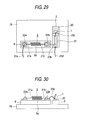
- Fig. 29 is a top view of a main portion of the conventional optical element module shown in Fig. 28.
- Fig. 30 is a side view of the main portion shown in Fig. 29.
- reference numerals 19, 20, and 5a respectively designate a base carrier for placing the light emitting element carrier 2 and the light receiving element carrier 4, a pattern formed on the light emitting element carrier 2, and an air-core coil as a central portion of the filter 5.
- Reference numerals 21a and 21b designate connecting portions extending from one end and the other end of this air-core coil 5a.
- the filter 5 is constructed by this air-core coil 5a and the connecting portions 21a and 21b.
- Reference numerals 22a and 22b respectively designate solder joining portions for soldering and joining the connecting portions 21a and 21b to the filter substrate 6.
- Reference numeral 23a designates a bonding wire for making an electrical connection between the electrode 15 for bias and the solder joining portion 22a.
- Reference numeral 23b designates a bonding wire for making an electrical connection between the solder joining portion 22b and the pattern 20.
- Reference numeral 23c designates a bonding wire for making an electrical connection between the pattern 20 and the light emitting element 1.
- Reference numeral 23d designates a bonding wire for making an electrical connection between the pattern 20 and the electrode for high frequency.
- the conventional optical element module is constructed as mentioned above.
- An RF signal transmitted from an unillustrated driver IC is inputted to the light emitting element 1 via the electrode 13 for high frequency, the bonding wire 23d, the pattern 20 and the bonding wire 23c.
- a direct current (DC) for supplying the bias electric current from the power source to the light emitting element 1 is inputted to the light emitting element 1 via the electrode 15 for bias, the bonding wire 23a, the solder j joining portion 22a, the connecting portion 21a, the air-core coil 5a, the connecting portion 21b, the solder joining portion 22b, the bonding wire 23b, the pattern 20 and the bonding wire 23c.
- a bias circuit for supplying power is generally arranged in the optical element module in addition to a circuit for supplying the RF signal.
- the air-core coil 5a is a noise countermeasure part used in this bias circuit, and functions as a filter for preventing the RF signal from being transmitted to the bias circuit.
- the air-core coil 5a is widely used as a part for the bias circuit for the following reasons, etc. Namely, (1) compactness can be realized by a precise winding technique, (2) the electric current flowing through the air-core coil 5a can be increased since the air-core coil 5a has low direct current resistance, and (3) the RF signal can be prevented in a wide band since parasitic capacity is small and self resonance frequency is high.
- the optical element module of 10 Gbps or more is required instead of the conventional optical element module of 2.5 Gbps.
- the length of a line path (the total of lengths of the connecting portion 21b, the solder joining portion 22b, the bonding wire 23b, the pattern 20 and the bonding wire 23c) between the light emitting element 1 and the bias circuit (the air-core coil 5a in this case) is longer than 1/4 of an upper limit frequency wavelength in a passing band
- the resonance frequency of the line path itself between the light emitting element 1 and the bias circuit lies within this passing band. Therefore, the passing band is limited by this resonance. It is necessary to set the line path length between the light emitting element 1 and one end of the air-core coil 5a to about 1 mm or less so as to cope with the recent high speed of 10 Gbps or more.
- the filter substrate 6 mounting the air-core coil 5a thereto is mounted in the vicinity of the light emitting element 1, and the light emitting element 1 and the air-core coil 5a are electrically connected to each other by the bonding wires 23b, 23c, etc. Therefore, a problem exists in that it is difficult to set the line path length between the light emitting element 1 and the air-core coil 5a to about 1 mm or less, and no preferable high frequency characteristics are obtained.
- This invention is made to solve the above problem, and an object of this invention is to provide an optical element module able to obtain preferable high frequency characteristics by shortening the line path length between the light emitting element 1 and the air-core coil 5a.
- An optical element module in this invention comprises a light emitting element; and a filter portion used in one portion of a bias circuit for supplying a bias electric current from a power source to this light emitting element; wherein this filter portion has a coil portion and a first connecting portion extending from one end of this coil portion; and the first connecting portion directly connects the coil portion and the light emitting element without electrically joining the first connecting portion to any substrate on the way.
- the coil portion and the light emitting element are connected to each other by thermocompression-bonding a one-side end portion of the first connecting portion to the light emitting element.
- the light emitting element has a metallic electrode on its surface, and a one-side end portion of the first connecting portion is constructed by forming a metallic film on a lead wire, and the coil portion and the light emitting element are connected to each other by joining the one-side end portion having the metallic film to the metallic electrode.
- the light emitting element has a metallic electrode on its surface, and the coil portion and the light emitting element are connected to each other by fixing a one-side end portion of the first connecting portion to this metallic electrode by a bump.
- the one-side end portion of the first connecting portion is constructed by forming a metallic film on a lead wire.
- the first connecting portion has a length shorter than 1/4 of a wavelength corresponding to an upper limit frequency of a high frequency signal supplied to the light emitting element.
- the first connecting portion has a length of 1 mm or less.
- an optical element module comprises a package; a feed-through for electrically conducting the interior and the exterior of this package, and having a shelf portion projected to the interior; a light emitting element included within the package; and a filter portion used in one portion of a bias circuit for supplying a bias electric current from a power source to the light emitting element; wherein this filter portion has a coil portion and a first connecting portion extending from one end of this coil portion, and also has a second connecting portion extending from the other end of the coil portion; the first connecting portion directly connects the coil portion and the light emitting element without electrically joining the first connecting portion to any substrate on the way; and the second connecting portion directly connects the other end of the coil portion and the shelf portion of the feed-through without electrically joining the second connecting portion to any substrate on the way.
- a filter portion for low frequency is arranged in the shelf portion of the feed-through, and is electrically connected in series to the coil through the second connecting portion.
- the light emitting element has a gold electrode on its surface, and the filter portion is constructed by one copper wire, and an insulating film is formed on the coil portion, and a gold film is formed on a one-side end portion of the first connecting portion, and the coil portion and the light emitting element are connected to each other by joining the one-side end portion having this gold film to the gold electrode of the light emitting element.
- an optical element module comprises a light emitting element; a substrate mounting this light emitting element thereto; and a filter portion used in one portion of a bias circuit for supplying a bias electric current from a power source to the light emitting element; wherein this filter portion has a coil portion and a first connecting portion extending from one end of this coil portion; and the first connecting portion directly connects the coil portion and the substrate mounting the light emitting element thereto without electrically joining the first connecting portion to any substrate on the way.
- the coil portion and the substrate mounting the light emitting element thereto are connected to each other by thermocompression-bonding a one-side end portion of the first connecting portion to the substrate mounting the light emitting element thereto.
- the substrate mounting the light emitting element thereto has a metallic pattern on its surface, and a one-side end portion of the first connecting portion is constructed by forming a metallic film on a lead wire, and the coil portion and the substrate mounting the light emitting element thereto are connected to each other by joining the one-side end portion having the metallic film to the metallic pattern.
- the substrate mounting the light emitting element thereto has a metallic pattern on its surface, and the coil portion and the substrate mounting the light emitting element thereto are connected to each other by fixing a one-side end portion of the first connecting portion to this metallic pattern by a bump.
- the one-side end portion of the first connecting portion is constructed by forming a metallic film on a lead wire.
- the length of a line path from one end of the coil portion to the light emitting element is shorter than 1/4 of a wavelength corresponding to an upper limit frequency of a high frequency signal supplied to the light emitting element.
- the length of a line path from one end of the coil portion to the light emitting element is set to 1 mm or less.
- an optical element module comprises a package; a feed-through for electrically conducting the interior and the exterior of this package, and having a shelf portion projected to the interior; a light emitting element included within the package; a substrate mounting this light emitting element thereto; and a filter portion used in one portion of a bias circuit for supplying a bias electric current from a power source to the light emitting element; wherein this filter portion has a coil portion and a first connecting portion extending from one end of this coil portion, and also has a second connecting portion extending from the other end of the coil portion; the first connecting portion directly connects the coil portion and the substrate mounting the light emitting element thereto without electrically joining the first connecting portion to any substrate on the way; and the second connecting portion directly connects the other end of the coil portion and the shelf portion of the feed-through without electrically joining the second connecting portion to any substrate on the way.
- a filter portion for low frequency is arranged in the shelf portion of the feed-through, and is electrically connected in series to the coil through the second connecting portion.
- the substrate mounting the light emitting element thereto has a gold pattern constructed by gold on its surface, and the filter portion is constructed by one copper wire, and an insulating film is formed on the coil portion, and a gold film is formed on a one-side end portion of the first connecting portion, and the coil portion and the substrate mounting the light emitting element thereto are connected to each other by joining the one-side end portion having this gold film to the gold pattern.
- Fig. 1 is a top view showing the structure of an optical element module in accordance with an embodiment mode 1 of this invention.
- reference numerals 11a and 11b respectively designate a shelf portion constituting one portion of a feed-through 11 and projected inside from a side wall of a package 9, and a shelf portion projected outside from the side wall of the package 9.
- An electrode 15 for bias is formed on surfaces of the shelf portions 11a and 11b, and electrically conducts the interior and the exterior of the package 9 through the side wall.
- Reference numeral 30 designates a filter portion used in one portion of a bias circuit for supplying a bias electric current from an unillustrated power source to a light emitting element 1.
- this filter portion 30 is connected to the light emitting element 1, and the other is connected to the electrode 15 for bias on the surface of the shelf portion 11a of the feed-through 11. Namely, in the optical element module in this embodiment mode 1, the filter portion 30 is laid and arranged between the light emitting element 1 and the feed-through 11. Therefore, no substrate for mounting the filter portion 30 exists.
- Fig. 2 is a top view of a main portion of the optical element module in accordance with the embodiment mode 1 shown in Fig. 1
- Fig. 3 is a side view of the main portion shown in Fig. 2.
- Fig. 3A is a side view showing a connecting situation of the filter portion 30 seen from a side of the feed-through 11
- Fig. 3B is a sectional view seen from a I-I section of Fig. 2.
- reference numerals 33, 35 and 37 respectively designate an air-core coil corresponding to a coil portion as a central portion of the filter portion 30, a first connecting portion extending from one end of this air-core coil 33, and a second connecting portion extending from the other end of the air-core coil 33.
- the first connecting portion 35 directly connects the air-core coil 33 and the light emitting element 1 without electrically joining the first connecting portion 35 to any substrate on the way.
- “electrically” means that a mechanical connection may be also made. Namely, there is also a case in which the filter portion 30 is mechanically joined (held) to a base carrier 19, a light emitting element carrier 2, etc.
- the filter portion 30 is heavy in weight, etc.
- the filter portion 30 is mechanically joined to the base carrier 19, the light emitting element carrier 2, etc. in the air-core coil 33, or the first connecting portion 35 and the second connecting portion 37.
- the second connecting portion 37 directly connects the air-core coil 33 and the electrode 15 for bias arranged on the surface of the shelf portion 11a of the feed-through 11 without electrically joining the second connecting portion 37 to any substrate on the way.
- the first connecting portion 35, the air-core coil 33 and the second connecting portion 37 are formed by constructing the air-core coil 33 by forming a spiral in an intermediate portion of one copper wire. Namely, no filter portion 30 has a cutting face on the way except for both ends of this filter portion 30.
- the first connecting portion 35 has a length shorter than 1/4 of a wavelength corresponding to an upper limit frequency of a high frequency signal supplied to the light emitting element 1. Namely, this length is set to 1 mm or less in consideration of the case of a high speed of 10 Gbps or more.
- the filter portion 30 is naturally arranged in an unobstructing position when back face light of the light emitting element 1 reaches a light receiving element 3.
- an electrode 13 for high frequency in the feed-through 11 forms a coplanar line path.
- a pattern 20 is a strip-shaped conductor, and the light emitting element carrier 2 is a dielectric substrate, and the base carrier 19 is a plane conductor plate. Therefore, the pattern 20, the light emitting element carrier 2 and the base carrier 19 function as a microstrip line path. This microstrip line path is connected by the coplanar line path of the feed-through 11 and a bonding wire 23d.
- Reference numeral 20x designates a ground conductor interposed between the light emitting element 1 and the light emitting element carrier 2, and connected to the plane conductor 19 by a VIA hole 20y.
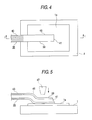
- Fig. 4 is an enlarged view in which a joining portion of the light emitting element 1 and the first connecting portion 35 in Fig. 2 is seen from a top face.
- Fig. 5 is a sectional view in a I-I section of the joining portion shown in Fig. 4.
- reference numerals 1a, 39 and 41 respectively designate a gold electrode as a metallic electrode formed on the surface of the light emitting element 1, a one-side end portion of the first connecting portion 35, and a copper wire as an example of a lead wire communicated over an entire length (the first connecting portion 35, the air-core coil 33 and the second connecting portion 37) of the filter portion 30 including this one-side end portion 39 without a cutting face.
- Reference numeral 43 designates an insulating film made by enamel and the copper wire 41 is coated with this insulating film 43. The insulating film 43 is formed in the air-core coil 33, one portion of the first connecting portion 35 and one portion of the second connecting portion 37.
- Reference numeral 45 designates gold plating as a metallic film formed on the copper wire 41 in a portion of the one-side end portion 39.
- the filter portion 30 has a construction having the air-core coil 33 between the first connecting portion 35 and the second connecting portion 37 by forming a spiral in an intermediate portion of the one copper wire 41 coated with the insulating film 43. Further, this filter portion 30 is constructed by removing at least the insulating film 43 on the surface of the one-side end portion 39 of the first connecting portion 35, and gold-plating the copper wire 41.
- the one-side end portion 39 having the gold plating 45 is joined to the gold electrode 1a by thermocompression bonding using an instrument, etc. widely used as a device and a jig for wire bonding such as a capillary 47.
- the air-core coil 33 and the light emitting element 1 are connected to each other by the first connecting portion 35 by this joining.
- temperature of the thermocompression bonding is set to about 150°C.
- the optical element module in this embodiment mode is constructed as mentioned above, it is possible to omit the solder joining portion 22b, the bonding wire 23b, the filter substrate 6, etc. conventionally arranged. Further, the light emitting element 1 and the air-core coil 33 can be directly joined to each other by the first connecting portion 35 without passing through the bonding wire 23c and the pattern 20. As a result, the distance between both the light emitting element 1 and the air-core coil 33 can be shortened. Therefore, it is possible to obtain an optical element module having preferable high frequency characteristics.
- the filter portion 30 in this embodiment mode is formed by one copper wire 41 over the entire length of this filter portion 30, and is constructed by gold-plating the surface of the one-side end portion 39 of the first connecting portion 35.
- the copper wire 41 is a hard raw material in comparison with gold. Therefore, there is an effect of easily making the air-core coil 33 by using the copper wire 41. Further, the gold wire is expensive and price of the air-core coil 33 is increased.
- the joining is performed without removing the insulating film 43 similarly to the air-core coil 33 instead of the gold plating 45 with respect to the one-side end portion 39.
- dielectric breakdown of the insulating film 43 formed on the one-side end portion 39 is performed at a high temperature such as about 300°C, and the one-side end portion 39 is pressurized and thermocompression-bonded to the gold electrode 1a of the light emitting element 1 so that the one-side end portion 39 is joined to the gold electrode 1a.
- this method is not suitable in a case in which the light emitting element 1 is weak in high temperature, etc.
- a method for joining the one-side end portion 39 of the first connecting portion 35 to the light emitting element 1 by resistance welding, soldering, etc. is also considered.
- the thermal load to the light emitting element 1 is large, and there is a possibility that the deterioration of characteristics is caused.
- the size of a jig for the joining is increased. Therefore, there is a possibility that it is difficult to perform the joining in a narrow range on an upper face of the light emitting element 1.
- the soldering there is a fear that solder flows out in the vicinity of the one-side end portion 39. Therefore, there is a possibility that the solder is attached to a light emitting point of the light emitting element 1.
- the joining method using the resistance welding, the soldering, etc. is not appropriate as a method for joining the one-side end portion 39 to the light emitting element 1.
- the constructing case of the filter portion 30 using one copper wire 41 has been explained in this embodiment mode.
- this invention is not limited to this case. Namely, it is sufficient to directly join the air-core coil 33 to the light emitting element 1 by the first connecting portion 35 without electrically joining the air-core coil 33 to any substrate on the way.
- the case for constructing the air-core coil 33 and the first connecting portion 35 by the copper wire 41 has been explained.
- the air-core coil 33 and the first connecting portion 35 may be also constructed by any lead wire formed by an electroconductive material having hardness equal to that of copper.
- the gold electrode 1a of the light emitting element 1 and the gold plating of the one-side end portion 39 are also examples of materials considered as optimum materials. Accordingly, a metallic electrode and a metallic film formed by another metal may be also used instead of gold if a similar role is fulfilled.
- unillustrated drive ICs are arranged in the exterior of the package 9 .
- this invention is not limited to this case. Namely, these drive ICs may be also included within the package 9.
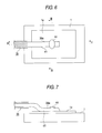
- FIG. 6 is an enlarged view in which a joining portion of the light emitting element 1 and the first connecting portion 35 in Fig. 2 is seen from a top face.
- Fig. 7 is a sectional view seen from a II-II section of the joining portion shown in Fig. 6.
- Fig. 8 is a sectional view seen from a III-III section of the joining portion shown in Fig. 6.
- This embodiment mode 2 differs from the embodiment mode 1 only in a thermocompression bonding method of the first connecting portion 35 and the light emitting element 1, and the others points are similar to those in the embodiment mode 1.
- reference numeral 39a designates a one-side end portion of the first connecting portion 35. However, no surface of this one-side end portion 39a is gold-plated, but a copper wire 41 is exposed to this surface.
- Reference numeral 44 designates a gold bump as an example of the bump.
- the one-side end portion 39a is pressed and joined to the gold electrode 1a by this gold bump 44 in an exposure portion of the copper wire 41.
- the one-side end portion 39a and the gold electrode 1a can be also joined to each other by such pressing of the gold bump 44. In this case, the joining can be also performed by using a capillary 47, etc.
- the copper wire 41 is more firmly joined to the gold electrode 1a by joining the gold bump 44 and the gold electrode 1a.
- the gold bump 44 and the gold electrode 1a are electrically conducted by joining the gold bump 44 and the gold electrode 1a to each other.
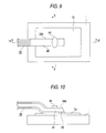
- FIG. 9 is an enlarged view in which a joining portion of the light emitting element 1 and the first connecting portion 35 in Fig. 2 is seen from a top face.
- Fig. 10 is a sectional view seen from a IV-IV section of the joining portion shown in Fig. 9.
- Fig. 11 is a sectional view seen from a V-V section of the joining portion shown in Fig. 9.
- This embodiment mode 3 differs from the embodiment mode 1 only in a thermocompression bonding method of the first connecting portion 35 and the light emitting element 1, and the others points are similar to those in the embodiment mode 1.
- reference numeral 39b designates a one-side end portion of the first connecting portion 35, and gold-plating 45 is formed on the surface of this one-side end portion 39b.
- Reference numeral 44 designates a gold bump as an example of the bump.
- the one-side end portion 39b is pressed and joined to the gold electrode 1a by this gold bump 44 in a forming portion of the gold plating 45.
- the one-side end portion 39b and the gold electrode 1a can be also joined to each other by forming the gold plating 45 on the copper wire 41 and then further pressing the gold bump 44.
- the joining can be also performed by using a capillary, etc.
- the gold plating 45 and the gold electrode 1a are also joined to each other in addition to the joining of the gold bump 44 and the gold electrode 1a. Therefore, the copper wire 41 is more firmly joined to the gold electrode 1a in comparison with the above embodiment mode 2. In addition to the joining between the gold bump 44 and the gold electrode 1a, the copper wire 41 is also electrically conducted to the gold electrode 1a by the joining of the gold plating 45 and the gold electrode 1a.
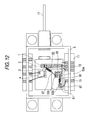
- Fig. 12 is a top view showing the structure of an optical element module in accordance with an embodiment mode 4 of this invention.
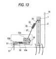
- Fig. 13 is a top view showing a main portion of the optical element module shown in Fig. 12.
- reference numerals 50 and 51 respectively designate a filter portion for low frequency, and a filter substrate for mounting this filter portion 50 for low frequency and manufactured by alumina.
- the filter portion 50 for low frequency may be constructed by an air-core coil, but may be also constructed by a chip inductor. Both ends of the filter portion 50 for low frequency are joined to the filter substrate 51 in solder joining portions 53a and 53b.
- the filter portion 30 functions as a filter portion for high frequency.
- solder joining portion 53c An end portion of a second connecting portion 37 of this filter portion 30 for high frequency is joined to the filter substrate 51 by a solder joining portion 53c.
- this solder joining portion 53c is electrically connected to the solder joining portion 53a by a third connecting portion 55.
- the solder joining portion 53b is also electrically connected to an electrode 15 for bias by a fourth connecting portion 57.
- the filter portion 50 for low frequency is electrically connected in series to the air-core coil 33 of the filter portion 30 through the second connecting portion 37.
- the problem of resonance as a subject of this invention mainly depends on the length of a line path between the light emitting element 1 and the air-core coil 33 near the light emitting element 1. Accordingly, high frequency characteristics can be improved in comparison with the conventional case by dividing the filter portion into two portions for high and low frequencies, and directly connecting the first connecting portion 35 of the filter portion 30 for high frequency near the light emitting element 1 to the light emitting element 1 without electrically joining the first connecting portion 35 to any substrate on the way as in this embodiment mode.
- “electrically” means that a mechanical connection may be also made. Namely, when the filter portion 30 is heavy in weight, there is a case in which the filter portion 30 is mechanically joined (held) to a base carrier 19, a light emitting element carrier 2, etc. by an adhesive, etc. In this case, the filter portion 30 is mechanically joined to the base carrier 19, the light emitting element carrier 2, etc. in the air-core coil 33, or the first connecting portion 35 and the second connecting portion 37.
- this embodiment mode 4 portions different from those in the optical element module shown in the embodiment mode 1 are explained, and explanations of the same or corresponding portions are omitted. Further, in this embodiment mode 4, the above embodiment mode 2 or 3 can be also adopted with respect to the joining method of the first connecting portion 35 and the light emitting element 1.
- Fig. 14 is a top view showing the structure of an optical element module in accordance with an embodiment mode 5 of this invention.
- Fig. 15 is a top view showing a main portion of the optical element module shown in Fig. 14.
- reference numeral 50a designates a filter portion for low frequency.
- This filter portion for low frequency may be constructed by an air-core coil, but may be also constructed by a chip inductor.
- This filter portion 50a for low frequency is arranged on a shelf portion 11a of a feed-through 11. Both ends of this filter portion 50a for low frequency are joined onto the shelf portion 11a by solder joining portions 53e and 53f.
- a filter portion 30 functions as a filter portion for high frequency.
- a second connecting portion 37 of this filter portion 30 for high frequency is joined to a portion near the solder joining portion 53f on the shelf portion 11a. Further, the solder joining portion 53e is connected to an electrode 15 for bias. Namely, the filter portion 50a for low frequency is electrically connected in series to the air-core coil 33 of the filter portion 30 through the second connecting portion 37.
- the problem of resonance as a subject of this invention mainly depends on the length of a line path between the light emitting element 1 and the air-core coil 33 near the light emitting element 1. Accordingly, high frequency characteristics can be improved in comparison with the conventional case by dividing the filter portion into two portions for high and low frequencies, and directly connecting the first connecting portion 35 of the filter portion 30 for high frequency near the light emitting element 1 to the light emitting element 1 without electrically joining the first connecting portion 35 to any substrate on the way as in this embodiment mode.
- the filter portion 50a for low frequency is arranged on the shelf portion 11a of the feed-through 11. Therefore, there is also an effect of being able to omit the filter substrate 51 in comparison with the embodiment mode 4.
- this embodiment mode 4 portions different from those in the optical element module shown in the embodiment mode 1 are explained, and explanations of the same or corresponding portions are omitted. Further, in this embodiment mode 5, the above embodiment mode 2 or 3 can be also adopted with respect to the joining method of the first connecting portion 35 and the light emitting element 1.
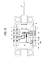
- Fig. 16 is a top view showing the structure of an optical element module in accordance with an embodiment mode 6 of this invention.
- reference numeral 30a designates a filter portion used in one portion of a bias circuit for supplying a bias electric current from a power source to the light emitting element 1.
- One end of this filter portion 30a is connected to a light emitting element carrier 2 as a substrate mounting the light emitting element 1 thereto, and the other end is connected to an electrode 15 for bias on the surface of a shelf portion 11a of the feed-through 11.
- Reference numeral 50a designates a filter portion for low frequency connected to this electrode 15 for bias, but a chip inductor is used here as this filter portion 50a for low frequency. This filter portion 50a for low frequency can be also omitted.
- the filter portion 30a is laid and arranged between the light emitting element carrier 2 and the feed-through 11. Therefore, there is also no conventionally existing substrate for mounting the filter portion 30a in this embodiment mode.
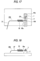
- Fig. 17 is a top view of a main portion of the optical element module in accordance with the embodiment mode 6 shown in Fig. 16.
- Fig. 18 is a side view of the main portion shown in Fig. 16.
- each of reference numerals 60a and 60b designates a gold pattern as a metallic pattern formed on the surface of the light emitting element carrier 2.
- the light emitting element 1 is placed on an upper face of this gold pattern 60a.
- the light emitting element 1 and the gold pattern 60b are connected to each other by a bonding wire 23c. Details of a microstrip line path, etc. are similar to those in Figs. 2 and 3.
- Reference numerals 33 and 35a respectively designate an air-core coil corresponding to a coil portion as a central portion of the filter portion 30a, and a first connecting portion extending from one end of this air-core coil 33. An end portion of this first connecting portion 35a is joined to the gold pattern 60b by thermocompression bonding.
- Reference numeral 37 designates a second connecting portion extending from the other end of the air-core coil 33.
- the first connecting portion 35a directly connects the air-core coil 33 and the light emitting element carrier 2 as a substrate mounting the light emitting element 1 thereto without electrically joining the first connecting portion 35a to any substrate on the way.
- the second connecting portion 37 directly connects the air-core coil 33 and the electrode 15 for bias arranged on the surface of the shelf portion 11a of the feed-through 11 without electrically joining the second connecting portion 37 to any substrate on the way.
- the length of a line path from one end of the air-core coil 33 to the light emitting element 1, i.e., the total of a length of the first connecting portion 35a and lengths of the gold pattern 60b and the bonding wire 23c is shorter than 1/4 of a wavelength corresponding to an upper limit frequency of a high frequency signal supplied to the light emitting element 1. Namely, this length is set to 1 mm or less in consideration of a high speed of 10 Gbps or more.
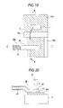
- Fig. 19 is an enlarged view in which a joining portion of the light emitting element carrier 2 and the first connecting portion 35a in Fig. 17 is seen from a top face.
- Fig. 20 is a sectional view in a I-I section of the joining portion shown in Fig. 19.
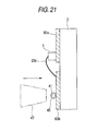
- Fig. 21 is a sectional view in a II-II section of the joining portion shown in Fig. 19.
- reference numeral 39 designates a one-side end portion of the first connecting portion 35a, and this one-side end portion 39 is thermocompression-bonded to the gold pattern 60b.
- Reference numeral 41 designates a copper wire communicated over an entire length (the first connecting portion 35a, the air-core coil 33 and the second connecting portion 37) of the filter portion 30 including this one-side end portion 39 without a cutting face. This copper wire 41 is coated with an insulating film 43. The insulating film 43 is formed in the air-core coil 33, one portion of the first connecting portion 35a and one portion of the second connecting portion 37.
- Reference numeral 45 designates gold plating as a metallic film formed in the copper wire 41 in a portion of the one-side end portion 39.
- the filter portion 30a has a construction having the air-core coil 33 between the first connecting portion 35a and the second connecting portion 37 by forming a spiral in an intermediate portion of the one copper wire 41 coated with the insulating film 43. Further, this filter portion 30a is constructed by removing at least the insulating film 43 on the surface of the one-side end portion 39 of the first connecting portion 35a, and forming the gold-plating 45 on the copper wire 41.
- the one-side end portion 39 having the gold plating 45 is joined to the gold pattern 60b by thermocompression bonding using an instrument, etc. widely used as a device and a jig for wire bonding such as a capillary 47.
- the air-core coil 33 and the light emitting element carrier 2 are connected to each other by the first connecting portion 35a by this joining.
- Temperature of the thermocompression bonding is set to about 150°C, and a supersonic wave can be also used together in the joining.
- the optical element module in this embodiment mode is constructed as mentioned above, it is possible to omit the solder joining portion 22b, the bonding wire 23b, etc. conventionally arranged. Therefore, the light emitting element carrier 2 and the air-core coil 33 can be directly j joined to each other by the first connecting portion 35a, and the distance between both the light emitting element carrier 2 and the air-core coil 33 can be shortened. As a result, it is possible to obtain an optical element module having preferable high frequency characteristics.
- the filter portion 30 in this embodiment mode is formed by one copper wire 41 over the entire length of this filter portion 30, and is constructed by forming gold-plating 45 on the surface of the one-side end portion 39 of the first connecting portion 35a. This is because it is considered that, when all of the first connecting portion 35a is constructed by gold wire, the first connecting portion 35a is too soft to form the air-core coil 33. Therefore, there is an effect of easily making the air-core coil 33 by using the copper wire 41. Further, the gold wire is expensive and price of the air-core coil 33 is increased.
- the joining can be performed by using a device and a jig (capillary 47, etc.) for wire bonding widely executed so that time and cost required in the joining can be reduced.
- the case for joining the one-side end portion 39 of the first connecting portion 35a to the gold pattern 60b connected to the light emitting element 1 by the bonding wire 23c has been explained.
- this invention is not limited to this case. Namely, if the gold pattern is arranged on the light emitting element carrier 2, the one-side end portion 39 may be also j joined to the gold pattern 60a placing the light emitting element 1 thereon. Further, the pattern is not limited to gold, but may be also set to aluminum.
- a filter portion 50 for low frequency is also used and variations of constructions as shown in the embodiment modes 4 and 5 can be made in this embodiment mode. Namely, similar to Fig. 12, the filter portion 50 for low frequency is mounted to a filter substrate 51, and an end portion of the second connecting portion 37 of the filter portion 30 can be electrically connected to one end of this filter portion 50 for low frequency. In accordance with such a construction, the filter portion 50 for low frequency is electrically connected in series to the air-core coil 33 of the filter portion 30 through the second connecting portion 37.
- the filter portion 50a for low frequency is arranged in a shelf portion 11a of the feed-through 11, and one end of this filter portion 50a for low frequency and an end portion of the second connecting portion 37 can be also connected to each other.
- the filter portion 50a for low frequency is electrically connected in series to the air-core coil 33 through the second connecting portion 37.
- FIG. 22 is an enlarged view in which a joining portion of the light emitting element carrier 2 and the first connecting portion 35a in Fig. 17 is seen from a top face.
- Fig. 23 is a sectional view seen from a III-III section of the joining portion shown in Fig. 22.
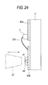
- Fig. 24 is a sectional view seen from a IV-IV section of the j oining portion shown in Fig. 22.
- This embodiment mode 7 differs from the embodiment mode 6 only in a thermocompression bonding method of the first connecting portion 35a and the light emitting element carrier 2, and the other points are similar to those in the embodiment mode 6.
- reference numeral 39a designates a one-side end portion of the first connecting portion 35a. However, no surface of this one-side end portion 39a is gold-plated, but a copper wire 41 is exposed to this surface.
- Reference numeral 44 designates a gold bump as an example of the bump.
- the one-side end portion 39a is pressed and joined to a gold pattern 60b by this gold bump 44 in an exposure portion of the copper wire 41.
- the one-side end portion 39a and the gold pattern 60b can be also joined to each other by such pressing of the gold bump 44. In this case, the joining can be also performed by using a capillary, etc.
- the copper wire 41 is more firmly joined to the gold pattern 60b by joining the gold bump 44 and the gold pattern 60b.
- the gold bump 44 and the gold pattern 60b are also electrically conducted by joining the gold bump 44 and the gold pattern 60b to each other.
- FIG. 25 is an enlarged view in which the joining portion of the light emitting element carrier 2 and the first connecting portion 35a in Fig. 17 is seen from the top face.
- Fig. 26 is a sectional view seen from a V-V section of the joining portion shown in Fig. 25.
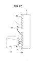
- Fig. 27 is a sectional view seen from a VI-VI section of the joining portion shown in Fig. 25.
- This embodiment mode 8 differs from the embodiment mode 6 only in a thermocompression bonding method of the first connecting portion 35a and the light emitting element carrier 2, and the other points are similar to those in the embodiment mode 6.
- reference numeral 39b designates a one-side end portion of the first connecting portion 35a, and gold-plating 45 is formed on the surface of this one-side end portion 39b.
- Reference numeral 44 designates a gold bump as an example of the bump.
- the one-side end portion 39b is pressed and joined to the gold pattern 60b by this gold bump 44 in a forming portion of the gold plating 45.
- the one-side end portion 39b and the gold pattern 60b can be also joined to each other by forming the gold plating 45 on the copper wire 41 and then further pressing the gold bump 44. In this case, the joining can be also performed by using a capillary, etc.
- the gold plating 45 and the gold pattern 60b are also joined to each other in addition to the joining of the gold bump 44 and the gold pattern 60b. Therefore, the copper wire 41 is more firmly joined to the gold pattern 60b in comparison with the above embodiment mode 7. In addition to the joining between the gold bump 44 and the gold pattern 60b, the copper wire 41 is electrically conducted to the gold pattern 60b by the joining of the gold plating 45 and the gold pattern 60b.
- An optical element module in this invention has a light emitting element, and a filter portion used in one portion of a bias circuit for supplying a bias electric current from a power source to this light emitting element, wherein this filter portion has a coil portion and a first connecting portion extending from one end of this coil portion, and the first connecting portion directly connects the coil portion and the light emitting element without electrically joining the first connecting portion to any substrate on the way. Accordingly, the length of a line path between the light emitting element and the coil is shortened and preferable high frequency characteristics can be obtained.
- an optical element module in this invention has a light emitting element, a substrate mounting this light emitting element thereto, and a filter portion used in one portion of a bias circuit for supplying a bias electric current from a power source to the light emitting element, wherein this filter portion has a coil portion and a first connecting portion extending from one end of this coil portion, and the first connecting portion directly connects the coil portion and the substrate mounting the light emitting element thereto without electrically joining the first connecting portion to any substrate on the way. Accordingly, the length of a line path between the light emitting element and the coil is shortened and preferable high frequency characteristics can be obtained.
Landscapes
- Physics & Mathematics (AREA)
- General Physics & Mathematics (AREA)
- Optics & Photonics (AREA)
- Optical Couplings Of Light Guides (AREA)
- Semiconductor Lasers (AREA)
Abstract
Description
Claims (20)
- An optical element module comprising:wherein this filter portion (30) has a coil portion (33) and a first connecting portion (35) extending from one end of this coil portion (33); anda light emitting element (1); anda filter portion (30) used in one portion of a bias circuit for supplying a bias electric current from a power source to this light emitting element (1);
said first connecting portion (35) directly connects said coil portion (33) and said light emitting element (1) without electrically joining the first connecting portion (35) to any substrate on the way. - An optical element module according to claim 1, wherein said coil portion (33) and said light emitting element (1) are connected to each other by thermocompression-bonding a one-side end portion (39) of the first connecting portion (35) to the light emitting element (1).
- An optical element module according to claim 1 or 2,
wherein the light emitting element (1) has a metallic electrode (1a) on its surface,
a one-side end portion (39) of the first connecting portion (35) is constructed by forming a metallic film on a lead wire, and
said coil portion (33) and said light emitting element (1) are connected to each other by joining the one-side end portion (39) having said metallic film to said metallic electrode (1a). - An optical element module according to claim 1 or 2,
wherein the light emitting element (1) has a metallic electrode (1a) on its surface, and
the coil portion (33) and said light emitting element (1) are connected to each other by fixing a one-side end portion (39) of the first connecting portion (35) to this metallic electrode (1a) by a bump (44). - An optical element module according to claim 4,
wherein the one-side end portion (39) of the first connecting portion (35) is constructed by forming a metallic film on a lead wire. - An optical element module according to any preceding claim,
wherein the first connecting portion (35) has a length shorter than 1/4 of a wavelength corresponding to an upper limit frequency of a high frequency signal supplied to the light emitting element (1). - An optical element module according to any preceding claim,
wherein the first connecting portion (35) has a length of 1 mm or less. - An optical element module comprising:wherein this filter portion (30) has a coil portion (33) and a first connecting portion (35) extending from one end of this coil portion (33), and also has a second connecting portion (37) extending from the other end of said coil portion (33);a package (9);a feed-through (11) for electrically conducting the interior and the exterior of this package (9), and having a shelf portion projected to said interior;a light emitting element (1) included within said package (9); anda filter portion (30) used in one portion of a bias circuit for supplying a bias electric current from a power source to said light emitting element (1);
said first connecting portion (35) directly connects said coil portion (33) and said light emitting element (1) without electrically joining the first connecting portion (35) to any substrate on the way; and
said second connecting portion (37) directly connects the other end of said coil portion (33) and the shelf portion of said feed-through (11) without electrically joining the second connecting portion (37) to any substrate on the way. - An optical element module according to claim 8,
wherein a filter portion (50) for low frequency is arranged in the shelf portion of the feed-through (11), and is electrically connected in series to the coil through the second connecting portion (37). - An optical element module according to claim 1,
wherein the light emitting element (1) has a gold electrode (6a) on its surface,
the filter portion (30) is constructed by one copper wire, and an insulating film is formed on the coil portion (33) , and a gold film is formed on a one-side end portion (39) of the first connecting portion (35), and
said coil portion (33) and said light emitting element (1) are connected to each other by joining the one-side end portion (39) having this gold film to the gold electrode (6a) of said light emitting element (1). - An optical element module comprising:wherein this filter portion (30) has a coil portion (33) and a first connecting portion (35) extending from one end of this coil portion (33); anda light emitting element (1);a substrate mounting this light emitting element (1) thereto; anda filter portion (30) used in one portion of a bias circuit for supplying a bias electric current from a power source to said light emitting element (1);
said first connecting portion (35) directly connects said coil portion (33) and said substrate mounting the light emitting element (1) thereto without electrically joining the first connecting portion (35) to any substrate on the way. - An optical element module according to claim 11,
wherein said coil portion (33) and said substrate mounting the light emitting element (1) thereto are connected to each other by thermocompression-bonding a one-side end portion (39) of the first connecting portion (35) to the substrate mounting the light emitting element (1) thereto. - An optical element module according to claim 11 or 12,
wherein the substrate mounting the light emitting element (1) thereto has a metallic pattern (1a) on its surface,
aone-side end portion (39) of the first connecting portion (35) is constructed by forming a metallic film on a lead wire, and
said coil portion (33) and said substrate mounting the light emitting element (1) thereto are connected to each other by joining the one-side end portion (39) having said metallic film to said metallic pattern (1a). - An optical element module according to claim 11 or 12,
wherein the substrate mounting the light emitting element (1) thereto has a metallic pattern (1a) on its surface, and
the coil portion (33) and said substrate mounting the light emitting element (1) thereto are connected to each other by fixing a one-side end portion (39) of the first connecting portion (35) to this metallic pattern (1a) by a bump (44). - An optical element module according to claim 14,
wherein the one-side end portion (39) of the first connecting portion (35) is constructed by forming a metallic film on a lead wire. - An optical element module according to any one of claims 11 to 15,
wherein the length of a line path from one end of the coil portion (33) to the light emitting element (1) is shorter than 1/4 of a wavelength corresponding to an upper limit frequency of a high frequency signal supplied to said light emitting element (1). - An optical element module according to any one of claims 11 to 16,
wherein the length of a line path from one end of the coil portion (33) to the light emitting element (1) is set to 1 mm or less. - An optical element module comprising:wherein this filter portion (30) has a coil portion (33) and a first connecting portion (35) extending from one end of this coil portion (33) , and also has a second connecting portion (37) extending from the other end of said coil portion (33) ;a package (9) ;a feed-through (11) for electrically conducting the interior and the exterior of this package (9), and having a shelf portion projected to said interior;a light emitting element (1) included within said package (9);a substrate mounting this light emitting element (1) thereto; anda filter portion (30) used in one portion of a bias circuit for supplying a bias electric current from a power source to said light emitting element (1);
said first connecting portion (35) directly connects said coil portion (33) and said substrate mounting the light emitting element (1) thereto without electrically joining the first connecting portion (35) to any substrate on the way; and
said second connecting portion (37) directly connects the other end of said coil portion (33) and the shelf portion of said feed-through (11) without electrically joining the second connecting portion (37) to any substrate on the way. - An optical element module according to claim 18,
wherein a filter portion (50) for low frequency is arranged in the shelf portion of the feed-through (11), and is electrically connected in series to the coil through the second connecting portion (37). - An optical element module according to claim 11,
wherein the substrate mounting the light emitting element (1) thereto has a gold pattern constructed by gold on its surface,
the filter portion (30) is constructed by one copper wire, and an insulating film is formed on the coil portion (33) , and a gold film is formed on a one-side end portion (39) of the first connecting portion (35), and
said coil portion (33) and said substrate mounting the light emitting element (1) thereto are connected to each other by joining the one-side end portion (39) having this gold film to said gold pattern.
Applications Claiming Priority (2)
| Application Number | Priority Date | Filing Date | Title |
|---|---|---|---|
| JP2001364450 | 2001-11-29 | ||
| JP2001364450A JP2003163403A (en) | 2001-11-29 | 2001-11-29 | Optical element module |
Publications (3)
| Publication Number | Publication Date |
|---|---|
| EP1324441A2 true EP1324441A2 (en) | 2003-07-02 |
| EP1324441A3 EP1324441A3 (en) | 2004-01-21 |
| EP1324441B1 EP1324441B1 (en) | 2006-06-07 |
Family
ID=19174641
Family Applications (1)
| Application Number | Title | Priority Date | Filing Date |
|---|---|---|---|
| EP02256083A Expired - Lifetime EP1324441B1 (en) | 2001-11-29 | 2002-09-02 | Optical element module |
Country Status (4)
| Country | Link |
|---|---|
| US (1) | US6753615B2 (en) |
| EP (1) | EP1324441B1 (en) |
| JP (1) | JP2003163403A (en) |
| DE (1) | DE60212057T2 (en) |
Families Citing this family (2)
| Publication number | Priority date | Publication date | Assignee | Title |
|---|---|---|---|---|
| EP1647036B1 (en) * | 2003-07-11 | 2007-11-21 | Nxp B.V. | Inductive-system |
| US6940181B2 (en) * | 2003-10-21 | 2005-09-06 | Micron Technology, Inc. | Thinned, strengthened semiconductor substrates and packages including same |
Family Cites Families (13)
| Publication number | Priority date | Publication date | Assignee | Title |
|---|---|---|---|---|
| JPS63104391A (en) | 1986-10-21 | 1988-05-09 | Seiko Epson Corp | Semiconductor laser driving device |
| JP3067151B2 (en) * | 1990-03-13 | 2000-07-17 | 日本電気株式会社 | Photoelectric conversion element subcarrier |
| JP3218797B2 (en) | 1993-05-20 | 2001-10-15 | 株式会社日立製作所 | Method for manufacturing high-frequency circuit module |
| US6044097A (en) | 1993-06-30 | 2000-03-28 | Fujitsu Limited | Modulator integrated distributed feed-back laser diode module and device using the same |
| JP3047735B2 (en) * | 1994-05-16 | 2000-06-05 | 住友電気工業株式会社 | Optical receiving module and method of manufacturing the same |
| JP3199611B2 (en) * | 1995-08-09 | 2001-08-20 | 京セラ株式会社 | Optical semiconductor element storage package |
| JPH11288961A (en) | 1998-04-03 | 1999-10-19 | Kaijo Corp | Conductor connection method, conductor wiring method, and wire bonding method |
| JP3353718B2 (en) | 1998-09-14 | 2002-12-03 | 日本電気株式会社 | Optical communication module |
| KR20000034841A (en) | 1998-11-10 | 2000-06-26 | 윤종용 | RF input unit ofahigh speed optical module |
| JP2000196175A (en) * | 1998-12-28 | 2000-07-14 | Toshiba Corp | Subcarrier and semiconductor device |
| US6207950B1 (en) * | 1999-01-11 | 2001-03-27 | Lightlogic, Inc. | Optical electronic assembly having a flexure for maintaining alignment between optical elements |
| US6227724B1 (en) * | 1999-01-11 | 2001-05-08 | Lightlogic, Inc. | Method for constructing an optoelectronic assembly |
| JP4031605B2 (en) | 2000-03-13 | 2008-01-09 | ローム株式会社 | Surge-protected semiconductor laser and optical pickup |
-
2001
- 2001-11-29 JP JP2001364450A patent/JP2003163403A/en active Pending
-
2002
- 2002-08-28 US US10/229,118 patent/US6753615B2/en not_active Expired - Lifetime
- 2002-09-02 EP EP02256083A patent/EP1324441B1/en not_active Expired - Lifetime
- 2002-09-02 DE DE60212057T patent/DE60212057T2/en not_active Expired - Lifetime
Also Published As
| Publication number | Publication date |
|---|---|
| DE60212057T2 (en) | 2007-01-04 |
| JP2003163403A (en) | 2003-06-06 |
| US20030098507A1 (en) | 2003-05-29 |
| EP1324441A3 (en) | 2004-01-21 |
| US6753615B2 (en) | 2004-06-22 |
| EP1324441B1 (en) | 2006-06-07 |
| DE60212057D1 (en) | 2006-07-20 |
Similar Documents
| Publication | Publication Date | Title |
|---|---|---|
| CN102422193B (en) | Optical subassembly with optical device having ceramic pacakge | |
| US6836492B2 (en) | Laser-diode module, optical transceiver and fiber transmission system | |
| WO2004008593A1 (en) | Package for optical semiconductor | |
| WO2015046292A1 (en) | Electronic component housing package and electronic device | |
| US11973312B2 (en) | Semiconductor laser device | |
| EP1324441B1 (en) | Optical element module | |
| US7192201B2 (en) | Optical transmitting module having a de-coupling inductor therein | |
| JP2010034386A (en) | Optical semiconductor device | |
| JP3810276B2 (en) | Optical semiconductor element storage package | |
| WO2013042627A1 (en) | Electronic component mounting substrate, electronic component accommodating package and electronic device | |
| JP2001160598A (en) | Substrate for mounting semiconductor element and package for storing optical semiconductor element | |
| JP7036646B2 (en) | Packages for semiconductor devices and semiconductor devices | |
| JP2004228552A (en) | Optical module | |
| US12439516B2 (en) | Optical apparatus | |
| JP3206716B2 (en) | Semiconductor device and lead frame pair | |
| JP2006287962A (en) | High frequency transmitting/receiving module | |
| JP3374732B2 (en) | Semiconductor element module and semiconductor device | |
| JP3860831B2 (en) | Optical semiconductor element storage package | |
| JP2003078065A (en) | Substrate for mounting semiconductor element and package for storing optical semiconductor element | |
| JP2004253409A (en) | Optical semiconductor element storage package and optical semiconductor device | |
| JP2002016456A (en) | High frequency composite element | |
| JP2003133630A (en) | Semiconductor element storage package and semiconductor device | |
| JP2002314190A (en) | Optical semiconductor element storage package and optical semiconductor device | |
| JP3726718B2 (en) | Semiconductor device | |
| JP2003224324A (en) | Optical semiconductor element storage package and optical semiconductor device |
Legal Events
| Date | Code | Title | Description |
|---|---|---|---|
| PUAI | Public reference made under article 153(3) epc to a published international application that has entered the european phase |
Free format text: ORIGINAL CODE: 0009012 |
|
| AK | Designated contracting states |
Designated state(s): AT BE BG CH CY CZ DE DK EE ES FI FR GB GR IE IT LI LU MC NL PT SE SK TR |
|
| AX | Request for extension of the european patent |
Extension state: AL LT LV MK RO SI |
|
| PUAL | Search report despatched |
Free format text: ORIGINAL CODE: 0009013 |
|
| AK | Designated contracting states |
Kind code of ref document: A3 Designated state(s): AT BE BG CH CY CZ DE DK EE ES FI FR GB GR IE IT LI LU MC NL PT SE SK TR |
|
| AX | Request for extension of the european patent |
Extension state: AL LT LV MK RO SI |
|
| 17P | Request for examination filed |
Effective date: 20040406 |
|
| 17Q | First examination report despatched |
Effective date: 20040709 |
|
| AKX | Designation fees paid |
Designated state(s): DE FR GB IT SE |
|
| GRAP | Despatch of communication of intention to grant a patent |
Free format text: ORIGINAL CODE: EPIDOSNIGR1 |
|
| GRAS | Grant fee paid |
Free format text: ORIGINAL CODE: EPIDOSNIGR3 |
|
| RAP1 | Party data changed (applicant data changed or rights of an application transferred) |
Owner name: MITSUBISHI DENKI KABUSHIKI KAISHA |
|
| GRAA | (expected) grant |
Free format text: ORIGINAL CODE: 0009210 |
|
| AK | Designated contracting states |
Kind code of ref document: B1 Designated state(s): DE FR GB IT SE |
|
| PG25 | Lapsed in a contracting state [announced via postgrant information from national office to epo] |
Ref country code: IT Free format text: LAPSE BECAUSE OF FAILURE TO SUBMIT A TRANSLATION OF THE DESCRIPTION OR TO PAY THE FEE WITHIN THE PRESCRIBED TIME-LIMIT;WARNING: LAPSES OF ITALIAN PATENTS WITH EFFECTIVE DATE BEFORE 2007 MAY HAVE OCCURRED AT ANY TIME BEFORE 2007. THE CORRECT EFFECTIVE DATE MAY BE DIFFERENT FROM THE ONE RECORDED. Effective date: 20060607 |
|
| REG | Reference to a national code |
Ref country code: GB Ref legal event code: FG4D |
|
| REF | Corresponds to: |
Ref document number: 60212057 Country of ref document: DE Date of ref document: 20060720 Kind code of ref document: P |
|
| PG25 | Lapsed in a contracting state [announced via postgrant information from national office to epo] |
Ref country code: SE Free format text: LAPSE BECAUSE OF FAILURE TO SUBMIT A TRANSLATION OF THE DESCRIPTION OR TO PAY THE FEE WITHIN THE PRESCRIBED TIME-LIMIT Effective date: 20060907 |
|
| ET | Fr: translation filed | ||
| PLBE | No opposition filed within time limit |
Free format text: ORIGINAL CODE: 0009261 |
|
| STAA | Information on the status of an ep patent application or granted ep patent |
Free format text: STATUS: NO OPPOSITION FILED WITHIN TIME LIMIT |
|
| 26N | No opposition filed |
Effective date: 20070308 |
|
| REG | Reference to a national code |
Ref country code: GB Ref legal event code: 746 Effective date: 20080125 |
|
| PGFP | Annual fee paid to national office [announced via postgrant information from national office to epo] |
Ref country code: FR Payment date: 20140906 Year of fee payment: 13 |
|
| REG | Reference to a national code |
Ref country code: FR Ref legal event code: ST Effective date: 20160531 |
|
| PG25 | Lapsed in a contracting state [announced via postgrant information from national office to epo] |
Ref country code: FR Free format text: LAPSE BECAUSE OF NON-PAYMENT OF DUE FEES Effective date: 20150930 |
|
| PGFP | Annual fee paid to national office [announced via postgrant information from national office to epo] |
Ref country code: DE Payment date: 20160831 Year of fee payment: 15 Ref country code: GB Payment date: 20160831 Year of fee payment: 15 |
|
| REG | Reference to a national code |
Ref country code: DE Ref legal event code: R119 Ref document number: 60212057 Country of ref document: DE |
|
| GBPC | Gb: european patent ceased through non-payment of renewal fee |
Effective date: 20170902 |
|
| PG25 | Lapsed in a contracting state [announced via postgrant information from national office to epo] |
Ref country code: DE Free format text: LAPSE BECAUSE OF NON-PAYMENT OF DUE FEES Effective date: 20180404 Ref country code: GB Free format text: LAPSE BECAUSE OF NON-PAYMENT OF DUE FEES Effective date: 20170902 |