EP1324261A1 - Non-contact data carrier and method of fabricating the same - Google Patents
Non-contact data carrier and method of fabricating the same Download PDFInfo
- Publication number
- EP1324261A1 EP1324261A1 EP20020029038 EP02029038A EP1324261A1 EP 1324261 A1 EP1324261 A1 EP 1324261A1 EP 20020029038 EP20020029038 EP 20020029038 EP 02029038 A EP02029038 A EP 02029038A EP 1324261 A1 EP1324261 A1 EP 1324261A1
- Authority
- EP
- European Patent Office
- Prior art keywords
- semiconductor device
- conductive substrate
- contact data
- data carrier
- coil antenna
- Prior art date
- Legal status (The legal status is an assumption and is not a legal conclusion. Google has not performed a legal analysis and makes no representation as to the accuracy of the status listed.)
- Granted
Links
Images



Classifications
-
- G—PHYSICS
- G06—COMPUTING OR CALCULATING; COUNTING
- G06K—GRAPHICAL DATA READING; PRESENTATION OF DATA; RECORD CARRIERS; HANDLING RECORD CARRIERS
- G06K19/00—Record carriers for use with machines and with at least a part designed to carry digital markings
- G06K19/06—Record carriers for use with machines and with at least a part designed to carry digital markings characterised by the kind of the digital marking, e.g. shape, nature, code
- G06K19/067—Record carriers with conductive marks, printed circuits or semiconductor circuit elements, e.g. credit or identity cards also with resonating or responding marks without active components
- G06K19/07—Record carriers with conductive marks, printed circuits or semiconductor circuit elements, e.g. credit or identity cards also with resonating or responding marks without active components with integrated circuit chips
- G06K19/077—Constructional details, e.g. mounting of circuits in the carrier
- G06K19/07749—Constructional details, e.g. mounting of circuits in the carrier the record carrier being capable of non-contact communication, e.g. constructional details of the antenna of a non-contact smart card
- G06K19/0775—Constructional details, e.g. mounting of circuits in the carrier the record carrier being capable of non-contact communication, e.g. constructional details of the antenna of a non-contact smart card arrangements for connecting the integrated circuit to the antenna
-
- G—PHYSICS
- G06—COMPUTING OR CALCULATING; COUNTING
- G06K—GRAPHICAL DATA READING; PRESENTATION OF DATA; RECORD CARRIERS; HANDLING RECORD CARRIERS
- G06K19/00—Record carriers for use with machines and with at least a part designed to carry digital markings
- G06K19/06—Record carriers for use with machines and with at least a part designed to carry digital markings characterised by the kind of the digital marking, e.g. shape, nature, code
- G06K19/067—Record carriers with conductive marks, printed circuits or semiconductor circuit elements, e.g. credit or identity cards also with resonating or responding marks without active components
- G06K19/07—Record carriers with conductive marks, printed circuits or semiconductor circuit elements, e.g. credit or identity cards also with resonating or responding marks without active components with integrated circuit chips
- G06K19/077—Constructional details, e.g. mounting of circuits in the carrier
- G06K19/07749—Constructional details, e.g. mounting of circuits in the carrier the record carrier being capable of non-contact communication, e.g. constructional details of the antenna of a non-contact smart card
-
- H—ELECTRICITY
- H01—ELECTRIC ELEMENTS
- H01F—MAGNETS; INDUCTANCES; TRANSFORMERS; SELECTION OF MATERIALS FOR THEIR MAGNETIC PROPERTIES
- H01F41/00—Apparatus or processes specially adapted for manufacturing or assembling magnets, inductances or transformers; Apparatus or processes specially adapted for manufacturing materials characterised by their magnetic properties
- H01F41/02—Apparatus or processes specially adapted for manufacturing or assembling magnets, inductances or transformers; Apparatus or processes specially adapted for manufacturing materials characterised by their magnetic properties for manufacturing cores, coils, or magnets
- H01F41/04—Apparatus or processes specially adapted for manufacturing or assembling magnets, inductances or transformers; Apparatus or processes specially adapted for manufacturing materials characterised by their magnetic properties for manufacturing cores, coils, or magnets for manufacturing coils
- H01F41/041—Printed circuit coils
- H01F41/042—Printed circuit coils by thin film techniques
-
- H—ELECTRICITY
- H10—SEMICONDUCTOR DEVICES; ELECTRIC SOLID-STATE DEVICES NOT OTHERWISE PROVIDED FOR
- H10W—GENERIC PACKAGES, INTERCONNECTIONS, CONNECTORS OR OTHER CONSTRUCTIONAL DETAILS OF DEVICES COVERED BY CLASS H10
- H10W70/00—Package substrates; Interposers; Redistribution layers [RDL]
- H10W70/60—Insulating or insulated package substrates; Interposers; Redistribution layers
- H10W70/699—Insulating or insulated package substrates; Interposers; Redistribution layers for flat cards, e.g. credit cards
-
- H—ELECTRICITY
- H10—SEMICONDUCTOR DEVICES; ELECTRIC SOLID-STATE DEVICES NOT OTHERWISE PROVIDED FOR
- H10W—GENERIC PACKAGES, INTERCONNECTIONS, CONNECTORS OR OTHER CONSTRUCTIONAL DETAILS OF DEVICES COVERED BY CLASS H10
- H10W74/00—Encapsulations, e.g. protective coatings
- H10W74/01—Manufacture or treatment
- H10W74/019—Manufacture or treatment using temporary auxiliary substrates
-
- H—ELECTRICITY
- H01—ELECTRIC ELEMENTS
- H01F—MAGNETS; INDUCTANCES; TRANSFORMERS; SELECTION OF MATERIALS FOR THEIR MAGNETIC PROPERTIES
- H01F5/00—Coils
- H01F5/003—Printed circuit coils
-
- H—ELECTRICITY
- H01—ELECTRIC ELEMENTS
- H01F—MAGNETS; INDUCTANCES; TRANSFORMERS; SELECTION OF MATERIALS FOR THEIR MAGNETIC PROPERTIES
- H01F5/00—Coils
- H01F5/06—Insulation of windings
-
- H—ELECTRICITY
- H10—SEMICONDUCTOR DEVICES; ELECTRIC SOLID-STATE DEVICES NOT OTHERWISE PROVIDED FOR
- H10W—GENERIC PACKAGES, INTERCONNECTIONS, CONNECTORS OR OTHER CONSTRUCTIONAL DETAILS OF DEVICES COVERED BY CLASS H10
- H10W72/00—Interconnections or connectors in packages
- H10W72/50—Bond wires
- H10W72/551—Materials of bond wires
- H10W72/552—Materials of bond wires comprising metals or metalloids, e.g. silver
- H10W72/5522—Materials of bond wires comprising metals or metalloids, e.g. silver comprising gold [Au]
-
- H—ELECTRICITY
- H10—SEMICONDUCTOR DEVICES; ELECTRIC SOLID-STATE DEVICES NOT OTHERWISE PROVIDED FOR
- H10W—GENERIC PACKAGES, INTERCONNECTIONS, CONNECTORS OR OTHER CONSTRUCTIONAL DETAILS OF DEVICES COVERED BY CLASS H10
- H10W74/00—Encapsulations, e.g. protective coatings
-
- H—ELECTRICITY
- H10—SEMICONDUCTOR DEVICES; ELECTRIC SOLID-STATE DEVICES NOT OTHERWISE PROVIDED FOR
- H10W—GENERIC PACKAGES, INTERCONNECTIONS, CONNECTORS OR OTHER CONSTRUCTIONAL DETAILS OF DEVICES COVERED BY CLASS H10
- H10W90/00—Package configurations
- H10W90/701—Package configurations characterised by the relative positions of pads or connectors relative to package parts
- H10W90/751—Package configurations characterised by the relative positions of pads or connectors relative to package parts of bond wires
- H10W90/754—Package configurations characterised by the relative positions of pads or connectors relative to package parts of bond wires between a chip and a stacked insulating package substrate, interposer or RDL
-
- H—ELECTRICITY
- H10—SEMICONDUCTOR DEVICES; ELECTRIC SOLID-STATE DEVICES NOT OTHERWISE PROVIDED FOR
- H10W—GENERIC PACKAGES, INTERCONNECTIONS, CONNECTORS OR OTHER CONSTRUCTIONAL DETAILS OF DEVICES COVERED BY CLASS H10
- H10W90/00—Package configurations
- H10W90/701—Package configurations characterised by the relative positions of pads or connectors relative to package parts
- H10W90/751—Package configurations characterised by the relative positions of pads or connectors relative to package parts of bond wires
- H10W90/758—Package configurations characterised by the relative positions of pads or connectors relative to package parts of bond wires between a chip and a stacked discrete passive device
-
- Y—GENERAL TAGGING OF NEW TECHNOLOGICAL DEVELOPMENTS; GENERAL TAGGING OF CROSS-SECTIONAL TECHNOLOGIES SPANNING OVER SEVERAL SECTIONS OF THE IPC; TECHNICAL SUBJECTS COVERED BY FORMER USPC CROSS-REFERENCE ART COLLECTIONS [XRACs] AND DIGESTS
- Y10—TECHNICAL SUBJECTS COVERED BY FORMER USPC
- Y10T—TECHNICAL SUBJECTS COVERED BY FORMER US CLASSIFICATION
- Y10T436/00—Chemistry: analytical and immunological testing
- Y10T436/17—Nitrogen containing
Definitions
- the present invention relates to a non-contact data carrier and a method of fabricating the same.
- a non-contact data carrier is provided with a memory capable of storing various data and is capable of non-contact communication with external reader/writer.
- Non-contact data carriers are used for automatic package sorting, inventory control, commodity protection from theft, production management and distribution management.
- Such a non-contact data carrier is fabricated by the following procedure.
- An antenna pattern is formed by etching a metal foil, such as an aluminum foil, laminated to a substrate of a resin through a resist pattern.
- a jumping circuit is formed by forming conductive members on the back surface of the substrate and connecting the antenna pattern through through holes to the conductive members.
- An IC chip provided with bumps is located such that the bumps correspond to antenna connecting terminals, and the bumps are electrically connected to the antenna connecting terminals. Then, the antenna pattern and the IC chip are covered with a protective coating.
- the jumping circuit In fabricating this non-contact data carrier, the jumping circuit must be formed by connecting the antenna pattern and the conductive members through the through holes, the IC chip provided with the bumps must be located relative to the antenna connecting terminals, and the bumps formed on the back surface of the IC chip must be electrically connected to the antenna connecting terminals. Since the antenna pattern and the IC chip are separately manufactured, the cost of the non-contact data carrier is high.
- non-contact data carriers using a microwave of the 2.45 GHz frequency band cost 5 to 100 odd dollars ("Micro Stamp presented by Mitsui & Co., Ltd. http://www.mbd.co.jp/mc/rfid.00.html ").
- a non-contact data carrier comprises: a semiconductor device; a coil antenna having opposite ends; wires connecting the semiconductor device and the opposite ends of the coil antenna; and a sealing resin coating encapsulating the semiconductor device, the coil antenna and the wires therein.
- the semiconductor device is mounted on a semiconductor device mount substantially provided on the same plane as that of the coil antenna.
- a protective layer is formed on surfaces of the coil antenna and the semiconductor device mount opposite to the side of the sealing resin coating.
- a non-contact data carrier fabricating method comprises the steps of: preparing a conductive substrate; forming a first resist pattern layer provided with openings on one of the surfaces of the conductive substrate, and forming a second resist pattern layer provided with openings on the other surface of the conductive substrate; forming locating holes in the substrate by coating the first resist pattern layer with a protective film and etching the conductive substrate through the openings of the second resist pattern layer; forming a coil antenna having opposite ends, and a semiconductor device mount by removing the protective film from the first resist pattern layer and plating the conductive substrate through the openings of the first resist pattern layer; removing the first and the second resist pattern layer from the conductive substrate; fixedly mounting a semiconductor device on the semiconductor device mount and connecting the opposite ends of the coil antenna to the semiconductor device; encapsulating the semiconductor device, the coil antenna, the wires and the surroundings of the semiconductor device mount with a sealing resin coating; and removing the conductive substrate from the semiconductor device mount and the coil antenna.
- one of the surfaces of the conductive substrate is roughened by a sandblasting process to form irregularities therein before forming the fist resist pattern layer.
- an oxide film is formed on the roughened surface of the conductive substrate by using an oxidizing solution.
- a protective layer is formed on the surfaces of the coil antenna and the semiconductor device mount opposite to the side of the sealing resin coating after removing the conductive substrate from the semiconductor device mount and the coil antenna.
- a plurality of semiconductor devices and a plurality of coil antennas respectively corresponding to the semiconductor devices are formed on the conductive substrate, and the sealing resin coating is cut and divided into divisions, each including one of the semiconductor devices and the coil antenna corresponding to the semiconductor device after removing the conductive substrate from the semiconductor mounts and the coil antennas.
- the non-contact data carrier does not need any work for forming the jumping circuit by connecting the antenna pattern to the conductive member through the through holes, locating the IC chip with its bumps coincided with the antenna connecting terminals, or electrically connecting the bumps to the antenna connecting terminals. Since the non-contact data carrier can be fabricated by steps of simply placing the semiconductor device on the semiconductor device mount and connecting the semiconductor device to the coil antenna by the wires, the non-contact data carrier of the present invention can be manufactured at a low cost.
- the non-contact data carrier of the present invention is small and has a short communication distance, the communication distance can be extended by providing a label or a card of a tag body with a booster antenna when the non-contact data carrier is used as a tag.
- An antenna pattern having a proper inductance may be formed on the surface of the sealing resin coating or the protective layer or on both the surfaces of the sealing resin coating and the protective layer, and the antenna pattern may be used as a component of a booster antenna or a resonance circuit.
- the antennal pattern may be electrically connected through via holes or through holes to the coil antenna so that the antenna pattern may resonate with the coil antenna.
- An additional antenna may be formed without forming any via holes or through holes, a proper pattern may be formed on the antenna, and an insulating layer, such as the sealing resin coating or the protective layer, may be used as a component of capacitor, and those may be used for resonation.
- Fig. 1 is a sectional view of a non-contact data carrier according to the present invention and Fig. 2 is a plan view of the non-contact data carrier.
- the non-contact data carrier includes a semiconductor device 11, a coil antenna 12 surrounding the semiconductor device 11 and having opposite ends 12a and 12b, and wires 14 connecting the opposite ends 12a and 12b of the coil antenna 12 to the semiconductor device 11.
- the semiconductor device 11 is mounted on a semiconductor device mount 15 having substantially the same plane as that of the coil antenna 12.
- the semiconductor device 11, the coil antenna 12, the semiconductor device mount 15 and the wires 14 are encapsulated by a sealing resin coating 13.
- Fig. 3 shows a non-contact data carrier in a comparative example.
- a resonance circuit is formed by a coil antenna pattern 3 formed on a substrate 1 of a plastic material, and a capacitor connected to the coil antenna pattern 3 to receive and send out radio waves of a fixed frequency.
- a coil antenna pattern 3 formed on a substrate 1 of a plastic material
- a capacitor connected to the coil antenna pattern 3 to receive and send out radio waves of a fixed frequency.
- medium waves of 125 kHz and microwaves of 13.56 MHz and 2.45 GHz are used for communication.
- a jumping circuit is formed by connecting the coil antenna pattern 3 through through holes to a conductive member 4 formed on the back surface of the substrate 1.
- the connecting terminals 3c of the coil antenna pattern 3 are connected to bumps formed on the back surface of AN IC chip 2.
- a capacitor is included in the IC chip.
- the non-contact data carrier of the present invention does not need any work for forming a jumping circuit by connecting an antenna pattern to a conductive member through through holes, locating an IC chip with its bumps coincided with antenna connecting terminals, or electrically connecting the bumps to the antenna connecting terminals. Since the non-contact data carrier of the present invention needs simple steps of placing the semiconductor device on the semiconductor device mount, and connecting the electrodes of the semiconductor device to the opposite ends of the coil antenna by the wires, the non-contact data carrier of the present invention can be manufactured at a low cost as compared with the non-contact data carrier in a comparative example.
- Fig. 4 illustrates a first non-contact data carrier fabricating method according to the present invention.
- a conductive substrate 21 of a copper alloy, 42 alloy or a stainless steel, such as SUS430 or SUS304 (JIS) is prepared.
- a surface of the conductive substrate 21 on which a coil antenna is to be formed is roughened by sandblasting to form irregularities 21a therein.
- the surface provided with the irregularities 21a of the conductive substrate 21 is subjected to a separating layer forming process by oxidizing the surface having the irregularities 21a with a chromic acid solution (oxidizing solution) to form an oxide film 21b.
- the oxide film 21b facilitates the separation of a conductive metal film and a sealing resin coating, which are formed by later processes, from the conductive substrate 21 (Figs. 4(1) and 7).
- photosensitive resist layers of a dry film resist are formed on both the surfaces of the conductive substrate 21.
- the photosensitive resist layers are subjected to an exposure process and a developing process to form a first resist pattern layer 22 provided with openings 22a corresponding to a coil antenna and a semiconductor device mount for a non-contact data carrier on the surface treated for roughening and removal facilitation of the conductive substrate 21, and to form a second resist pattern 23 provided with openings 23a corresponding to locating holes on the other surface of the conductive substrate 21 (Fig. 4(2)).
- the dry film resist is a three-layer structure consisting of a base film, a resist film formed on the base film, and a protective coating film.
- the protective coating film is peeled off, the resist film is exposed to light.
- the dry film resist is applied to the conductive substrate 21 with the resist film in close contact with the surface of the conductive substrate 21, and then the base film is removed to form the photosensitive resist layer on the surface of the conductive substrate 21.
- the first resist pattern layer 22 and the second resist pattern layer 23 may be formed by a printing process, such as a screen printing process or a gravure printing process.
- the first resist pattern layer 22 formed on the conductive substrate 21 is coated with a corrosion-resistant protective film 24, such as a polyethylene terephthalate film (Fig. 4(3)).
- Parts of the conductive substrate 21 corresponding to the openings 23a of the second resist pattern layer 23 are etched to form locating holes 25 (Fig. 4(4)).
- the protective film 24 is removed, the first resist pattern layer 22 is exposed (Fig. 4(5)), and parts of the conductive substrate 21 corresponding to the openings 22a of the first resist pattern layer 22 are plated with a film of Au, Ag, Cu, Pd or Ni or with a multilayer film of some of those materials (Fig. 4(6)). Then, the first resist pattern layer 22 is immersed in a stripping liquid to remove the same from the conductive substrate 21, and then the conductive substrate 21 is subjected to a cleaning process or the like to complete a coil antenna 12 and a semiconductor device mount 15 (Fig. 4(7)). The second resist pattern layer 23 is removed together with the first resist pattern layer 22.
- a semiconductor device 11 is fixedly mounted on the semiconductor device mount 15 (Fig. 4(8)).
- the electrodes 11a of the semiconductor device 11 are connected to the opposite ends 12a and 12b of the coil antenna 12 by wire bonding using wires 14 of a noble metal, such as Au (Fig. 4(9)).
- the wire bonding using the wires 14 may be carried out by a wire bonding machine, such as a thermocompression wire bonder using only heating and compressing, a ultrasonic thermocompression wire bonder using heating, compressing and ultrasonic waves or a wedge bonder using only ultrasonic vibrations at an ordinary temperature.
- the coil antenna 12, the semiconductor device 11 and the wires 14 are encapsulated by a sealing resin coating 13 of an epoxy resin or the like (Fig. 4(10)).
- a sealing resin coating 13 of an epoxy resin or the like Fig. 4(10).
- the metal films forming the coil antenna 12 and the semiconductor device mount 15 can adhere firmly to the conductive substrate 21, withstand pressure, particularly, lateral pressure, that acts thereon during the molding process and therefore the coil antenna 12 and the semiconductor device mount 15, never come off the conductive substrate 21 because the surface the conductive substrate 21 on which the coil antenna 12 and the semiconductor device mount 15 are formed has irregularities 21a.
- the conductive substrate 21 is separated from the coil antenna 12 and the semiconductor device 11 sealed in the sealing resin coating 13 (Fig. 4(11)). Due to the surface treatment and the separating layer forming process for the surface of the conductive substrate 21, the conductive substrate 21 can easily be separated from the coil antenna 12 and the semiconductor device 11 by exerting a force perpendicularly to the conductive substrate 21.
- a modification of the first non-contact data carrier fabricating method will be described.
- a conductive substrate 21 of a copper alloy is used, and a coil antenna 12 and a semiconductor device mount 15 are formed by processing a two-layer film consisting of a Cu film and a Pd film.
- the conductive substrate 21 is dissolved selectively in a liquid capable of dissolving Cu and incapable of dissolving Pd.
- the rest of steps of the modification are the same as those of the first non-contact data carrier fabricating method.
- Figs. 5 and 6 illustrates a second non-contact data carrier fabricating method.
- a conductive substrate 31 of a copper alloy, 42 alloy or a stainless steel, such as SUS430 (JIS) is prepared.
- Asurface of the conductive substrate 31 on which a coil antenna is to be formed is roughened by sandblasting to form irregularities 31a therein.
- the surface provided with the irregularities 31a of the conductive substrate 31 is subjected to a separating layer forming process by oxidizing the surface having the irregularities 31a with a chromic acid solution (oxidizing solution) to form an oxide film 31b.
- the oxide film 31b facilitates the separation of a conductive metal film and a sealing resin coating, which are formed by later processes, from the conductive substrate 31 (Figs. 5(1) and 8).
- photosensitive resist layers are formed on both the surfaces of the conductive substrate 31 by using a dry film resist.
- the photosensitive resist layers are subjected to an exposure process and a developing process to form a first resist pattern layer 32 provided with openings 32a corresponding to a plurality of coil antennas and a plurality of semiconductor device mounts for a plurality of non-contact data carriers on the surface treated for roughening and removal facilitation of the conductive substrate 31, and to form a second resist pattern layer 33 provided with openings 33a corresponding to locating holes on the other surface of the conductive substrate 31 (Fig. 5(2)).
- the first resist pattern layer 32 and the second resist pattern layer 33 may be formed by a printing process, such as a screen printing process or a gravure printing process.
- the first resist pattern layer 32 formed on the conductive substrate 31 is coated with a corrosion-resistant protective film 34, such as a polyethylene terephthalate film (Fig. 5(3)).
- Parts of the conductive substrate 31 corresponding to the openings 33a of the second resist pattern layer 33 are etched to form locating holes 35 (Fig. 5(4)).
- the protective film 34 is removed, the first resist pattern layer 32 is exposed (Fig. 5(5)), and parts of the conductive substrate 31 corresponding to the openings 32a of the first resist pattern layer 32 are plated with a film of Au, Ag, Cu, Pd or Ni or with a multilayer film of some of those materials (Fig. 5(6)). Then, the first resist pattern layer 32 is immersed in a stripping liquid to remove the same from the conductive substrate 31, and then the conductive substrate 31 is subjected to a cleaning process or the like to complete coil antennas 12 and semiconductor device mounts 15 (Fig. 5(7)). The second resist pattern layer 33 is removed together with the first resist pattern layer 32.
- a plurality of semiconductor devices 11 are fixedly mounted on the semiconductor device mounts 15 (Fig. 6(1)), respectively.
- the plurality of semiconductor devices 11 correspond to the plurality of coil antennas 12 formed on the conductive substrate 31, respectively.
- the electrodes 11a of the semiconductor devices 11 are connected to the opposite ends 12a and 12b of the corresponding coil antennas 12, respectively, by wire bonding using wires 14 of a noble metal, such as Au (Fig. 6(2)).
- the coil antennas 12, the semiconductor devices 11 and the wires 14 are encapsulated by a sealing resin coating 13 of an epoxy resin or the like (Fig. 6(3)).
- the conductive substrate 31 is separated from the coil antennas 12 and the semiconductor devices 11 sealed in the sealing resin coating 13, and the respective surfaces of the coil antennas 12 and the semiconductor device mounts 15 opposite to the side of the sealing resin coating 13 are coated with a protective layer 16 of solder paste or the like (Fig. 6(4)).
- the sealing resin coating 13 and the protective layer 36 are cut into divisions, each including one of the semiconductor device 11 and one of the coil antenna 12 corresponding to the semiconductor device 11 (Fig. 6(5)).
- the second non-contact data carrier fabricating method is able to fabricate a plurality of non-contact data carriers efficiently simultaneously.
- a modification of the second non-contact data carrier fabricating method will be described.
- a conductive substrate 31 of a copper alloy is used, and coil antennas 12 and semiconductor device mounts 15 are formed by processing a two-layer film consisting of a Cu film and a Pd film.
- the conductive substrate 31 is dissolved selectively in a liquid capable of dissolving Cu and incapable of dissolving Pd.
- the rest of steps of the modification are the same as those of the second non-contact data carrier fabricating method.
- the communication distance of the non-contact data carrier of the present invention can be extended by applying a booster antenna to the non-contact data carrier.
- the non-contact data carrier of the present invention is characterized in that the semiconductor device and the coil antenna are sealed in the sealing resin coating, and that the semiconductor device is connected to the opposite ends of the coil antenna by the wires.
- the present invention does not need any work, that is needed by the conventional non-contact data carrier, for forming a jumping circuit by connecting an antenna pattern to a conductive member through through holes, locating an IC chip with its bumps coincided with antenna connecting terminals, or electrically connecting the bumps to the antenna connecting terminals.
- the non-contact data carrier of the present invention can be manufactured at a low cost as compared with the conventional non-contact data carrier.
- the non-contact data carrier fabricating method of the present invention comprises the steps of forming a coil antenna and a semiconductor device mount on a substrate, mounting a semiconductor device on a semiconductor device mount, and connecting the electrodes of the semiconductor device to the opposite ends of the coil antenna by wires.
- the non-contact data carrier fabricating method of the present invention does not need any work, that is needed by the conventional non-contact data carrier fabricating method, for forming a jumping circuit by connecting an antenna pattern to a conductive member through through holes, locating an IC chip with its bumps coincided with antenna connecting terminals, or electrically connecting the bumps to the antenna connecting terminals.
- the non-contact data carrier fabricating method of the present invention is able to fabricate the non-contact data carrier at a low manufacturing cost as compared with the conventional non-contact data carrier fabricating method.
Landscapes
- Engineering & Computer Science (AREA)
- Power Engineering (AREA)
- Microelectronics & Electronic Packaging (AREA)
- Computer Hardware Design (AREA)
- Physics & Mathematics (AREA)
- General Physics & Mathematics (AREA)
- Theoretical Computer Science (AREA)
- Manufacturing & Machinery (AREA)
- Credit Cards Or The Like (AREA)
- Details Of Aerials (AREA)
Abstract
Description
- The present invention relates to a non-contact data carrier and a method of fabricating the same.
- A non-contact data carrier is provided with a memory capable of storing various data and is capable of non-contact communication with external reader/writer. Non-contact data carriers are used for automatic package sorting, inventory control, commodity protection from theft, production management and distribution management.
- Such a non-contact data carrier is fabricated by the following procedure. An antenna pattern is formed by etching a metal foil, such as an aluminum foil, laminated to a substrate of a resin through a resist pattern. Then, a jumping circuit is formed by forming conductive members on the back surface of the substrate and connecting the antenna pattern through through holes to the conductive members. An IC chip provided with bumps is located such that the bumps correspond to antenna connecting terminals, and the bumps are electrically connected to the antenna connecting terminals. Then, the antenna pattern and the IC chip are covered with a protective coating.
- In fabricating this non-contact data carrier, the jumping circuit must be formed by connecting the antenna pattern and the conductive members through the through holes, the IC chip provided with the bumps must be located relative to the antenna connecting terminals, and the bumps formed on the back surface of the IC chip must be electrically connected to the antenna connecting terminals. Since the antenna pattern and the IC chip are separately manufactured, the cost of the non-contact data carrier is high.
- Thus, the manufacturing cost of non-contact data carriers is high. Although dependent on configuration, it is said that non-contact data carriers using a microwave of the 2.45 GHz frequency band cost 5 to 100 odd dollars ("Micro Stamp presented by Mitsui & Co., Ltd. http://www.mbd.co.jp/mc/rfid.00.html").
- It is an object of the present invention to provide a non-contact data carrier capable of being fabricated at a manufacturing cost lower than that of the conventional non-contact data carriers, and a method of fabricating the non-contact data carrier.
- According to one aspect of the present invention, a non-contact data carrier comprises: a semiconductor device; a coil antenna having opposite ends; wires connecting the semiconductor device and the opposite ends of the coil antenna; and a sealing resin coating encapsulating the semiconductor device, the coil antenna and the wires therein.
- In the non-contact data carrier according to the present invention, the semiconductor device is mounted on a semiconductor device mount substantially provided on the same plane as that of the coil antenna.
- In the non-contact data carrier according to the present invention, a protective layer is formed on surfaces of the coil antenna and the semiconductor device mount opposite to the side of the sealing resin coating.
- According to another aspect of the present invention, a non-contact data carrier fabricating method comprises the steps of: preparing a conductive substrate; forming a first resist pattern layer provided with openings on one of the surfaces of the conductive substrate, and forming a second resist pattern layer provided with openings on the other surface of the conductive substrate; forming locating holes in the substrate by coating the first resist pattern layer with a protective film and etching the conductive substrate through the openings of the second resist pattern layer; forming a coil antenna having opposite ends, and a semiconductor device mount by removing the protective film from the first resist pattern layer and plating the conductive substrate through the openings of the first resist pattern layer; removing the first and the second resist pattern layer from the conductive substrate; fixedly mounting a semiconductor device on the semiconductor device mount and connecting the opposite ends of the coil antenna to the semiconductor device; encapsulating the semiconductor device, the coil antenna, the wires and the surroundings of the semiconductor device mount with a sealing resin coating; and removing the conductive substrate from the semiconductor device mount and the coil antenna.
- In the non-contact data carrier fabricating method according to the present invention, one of the surfaces of the conductive substrate is roughened by a sandblasting process to form irregularities therein before forming the fist resist pattern layer.
- In the non-contact data carrier fabricating method according to the present invention, an oxide film is formed on the roughened surface of the conductive substrate by using an oxidizing solution.
- In the non-contact data carrier fabricating method according to the present invention, a protective layer is formed on the surfaces of the coil antenna and the semiconductor device mount opposite to the side of the sealing resin coating after removing the conductive substrate from the semiconductor device mount and the coil antenna.
- In the non-contact data carrier fabricating method according to the present invention, a plurality of semiconductor devices and a plurality of coil antennas respectively corresponding to the semiconductor devices are formed on the conductive substrate, and the sealing resin coating is cut and divided into divisions, each including one of the semiconductor devices and the coil antenna corresponding to the semiconductor device after removing the conductive substrate from the semiconductor mounts and the coil antennas.
- The non-contact data carrier does not need any work for forming the jumping circuit by connecting the antenna pattern to the conductive member through the through holes, locating the IC chip with its bumps coincided with the antenna connecting terminals, or electrically connecting the bumps to the antenna connecting terminals. Since the non-contact data carrier can be fabricated by steps of simply placing the semiconductor device on the semiconductor device mount and connecting the semiconductor device to the coil antenna by the wires, the non-contact data carrier of the present invention can be manufactured at a low cost.
- Although the non-contact data carrier of the present invention is small and has a short communication distance, the communication distance can be extended by providing a label or a card of a tag body with a booster antenna when the non-contact data carrier is used as a tag.
- An antenna pattern having a proper inductance may be formed on the surface of the sealing resin coating or the protective layer or on both the surfaces of the sealing resin coating and the protective layer, and the antenna pattern may be used as a component of a booster antenna or a resonance circuit. When such an antenna pattern is used, the antennal pattern may be electrically connected through via holes or through holes to the coil antenna so that the antenna pattern may resonate with the coil antenna. An additional antenna may be formed without forming any via holes or through holes, a proper pattern may be formed on the antenna, and an insulating layer, such as the sealing resin coating or the protective layer, may be used as a component of capacitor, and those may be used for resonation.
-
- Fig. 1 is a sectional view of a non-contact data carrier according to the present invention;
- Fig. 2 is a plan view of the non-contact data carrier according to the present invention;
- Fig. 3 is a plan view of a non-contact data carrier in a comparative example;
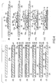
- Fig. 4 is sectional views of a workpiece in successive phases of a first non-contact data carrier fabricating method according to the present invention;
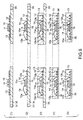
- Fig. 5 is sectional views of a workpiece in successive phases of a second non-contact data carrier fabricating method according to the present invention;
- Fig. 6 is sectional views of the non-contact data carrier in successive phases following those of the second non-contact data carrier fabricating method shown in Fig. 5;
- Fig. 7 is a side elevation of a substrate; and
- Fig. 8 is a side elevation of a substrate.
-
- Preferred embodiments of the present invention will be described with reference to the accompanying drawings.
- Fig. 1 is a sectional view of a non-contact data carrier according to the present invention and Fig. 2 is a plan view of the non-contact data carrier.
- Referring to Figs. 1 and 2, the non-contact data carrier includes a
semiconductor device 11, acoil antenna 12 surrounding thesemiconductor device 11 and havingopposite ends wires 14 connecting theopposite ends coil antenna 12 to thesemiconductor device 11. Thesemiconductor device 11 is mounted on asemiconductor device mount 15 having substantially the same plane as that of thecoil antenna 12. Thesemiconductor device 11, thecoil antenna 12, thesemiconductor device mount 15 and thewires 14 are encapsulated by a sealingresin coating 13. - Surfaces of the
coil antenna 12 and the semiconductor device mount 15 opposite to the side of the sealingresin coating 13 are covered for protection with aprotective layer 16 formed of a solder resist. - Fig. 3 shows a non-contact data carrier in a comparative example.
- In the non-contact data carrier shown in Fig. 3, a resonance circuit is formed by a
coil antenna pattern 3 formed on asubstrate 1 of a plastic material, and a capacitor connected to thecoil antenna pattern 3 to receive and send out radio waves of a fixed frequency. Generally, medium waves of 125 kHz and microwaves of 13.56 MHz and 2.45 GHz are used for communication. - In the non-contact data carrier shown in Fig. 3, a jumping circuit is formed by connecting the
coil antenna pattern 3 through through holes to aconductive member 4 formed on the back surface of thesubstrate 1. The connecting terminals 3c of thecoil antenna pattern 3 are connected to bumps formed on the back surface of ANIC chip 2. In the non-contact data carrier shown in Fig. 3, a capacitor is included in the IC chip. - As apparent from Fig. 1, the non-contact data carrier of the present invention does not need any work for forming a jumping circuit by connecting an antenna pattern to a conductive member through through holes, locating an IC chip with its bumps coincided with antenna connecting terminals, or electrically connecting the bumps to the antenna connecting terminals. Since the non-contact data carrier of the present invention needs simple steps of placing the semiconductor device on the semiconductor device mount, and connecting the electrodes of the semiconductor device to the opposite ends of the coil antenna by the wires, the non-contact data carrier of the present invention can be manufactured at a low cost as compared with the non-contact data carrier in a comparative example.
- Non-contact data carrier fabricating methods according to the present invention will be described. Fig. 4 illustrates a first non-contact data carrier fabricating method according to the present invention. Referring to Fig- 4, a
conductive substrate 21 of a copper alloy, 42 alloy or a stainless steel, such as SUS430 or SUS304 (JIS), is prepared. A surface of theconductive substrate 21 on which a coil antenna is to be formed is roughened by sandblasting to formirregularities 21a therein. The surface provided with theirregularities 21a of theconductive substrate 21 is subjected to a separating layer forming process by oxidizing the surface having theirregularities 21a with a chromic acid solution (oxidizing solution) to form anoxide film 21b. Theoxide film 21b facilitates the separation of a conductive metal film and a sealing resin coating, which are formed by later processes, from the conductive substrate 21 (Figs. 4(1) and 7). - Then, photosensitive resist layers of a dry film resist are formed on both the surfaces of the
conductive substrate 21. The photosensitive resist layers are subjected to an exposure process and a developing process to form a firstresist pattern layer 22 provided withopenings 22a corresponding to a coil antenna and a semiconductor device mount for a non-contact data carrier on the surface treated for roughening and removal facilitation of theconductive substrate 21, and to form asecond resist pattern 23 provided with openings 23a corresponding to locating holes on the other surface of the conductive substrate 21 (Fig. 4(2)). - Generally, the dry film resist is a three-layer structure consisting of a base film, a resist film formed on the base film, and a protective coating film. When the protective coating film is peeled off, the resist film is exposed to light. The dry film resist is applied to the
conductive substrate 21 with the resist film in close contact with the surface of theconductive substrate 21, and then the base film is removed to form the photosensitive resist layer on the surface of theconductive substrate 21. - The first resist
pattern layer 22 and the second resistpattern layer 23 may be formed by a printing process, such as a screen printing process or a gravure printing process. - Then, the first resist
pattern layer 22 formed on theconductive substrate 21 is coated with a corrosion-resistantprotective film 24, such as a polyethylene terephthalate film (Fig. 4(3)). - Parts of the
conductive substrate 21 corresponding to the openings 23a of the second resistpattern layer 23 are etched to form locating holes 25 (Fig. 4(4)). - Then, the
protective film 24 is removed, the first resistpattern layer 22 is exposed (Fig. 4(5)), and parts of theconductive substrate 21 corresponding to theopenings 22a of the first resistpattern layer 22 are plated with a film of Au, Ag, Cu, Pd or Ni or with a multilayer film of some of those materials (Fig. 4(6)). Then, the first resistpattern layer 22 is immersed in a stripping liquid to remove the same from theconductive substrate 21, and then theconductive substrate 21 is subjected to a cleaning process or the like to complete acoil antenna 12 and a semiconductor device mount 15 (Fig. 4(7)). The second resistpattern layer 23 is removed together with the first resistpattern layer 22. - Then, a
semiconductor device 11 is fixedly mounted on the semiconductor device mount 15 (Fig. 4(8)). - Then, the
electrodes 11a of thesemiconductor device 11 are connected to the opposite ends 12a and 12b of thecoil antenna 12 by wirebonding using wires 14 of a noble metal, such as Au (Fig. 4(9)). The wire bonding using thewires 14 may be carried out by a wire bonding machine, such as a thermocompression wire bonder using only heating and compressing, a ultrasonic thermocompression wire bonder using heating, compressing and ultrasonic waves or a wedge bonder using only ultrasonic vibrations at an ordinary temperature. - Then, the
coil antenna 12, thesemiconductor device 11 and thewires 14 are encapsulated by a sealingresin coating 13 of an epoxy resin or the like (Fig. 4(10)). During this molding process, the metal films forming thecoil antenna 12 and thesemiconductor device mount 15 can adhere firmly to theconductive substrate 21, withstand pressure, particularly, lateral pressure, that acts thereon during the molding process and therefore thecoil antenna 12 and thesemiconductor device mount 15, never come off theconductive substrate 21 because the surface theconductive substrate 21 on which thecoil antenna 12 and thesemiconductor device mount 15 are formed hasirregularities 21a. - Then, the
conductive substrate 21 is separated from thecoil antenna 12 and thesemiconductor device 11 sealed in the sealing resin coating 13 (Fig. 4(11)). Due to the surface treatment and the separating layer forming process for the surface of theconductive substrate 21, theconductive substrate 21 can easily be separated from thecoil antenna 12 and thesemiconductor device 11 by exerting a force perpendicularly to theconductive substrate 21. - Then, the respective surfaces of the
coil antenna 12 and thesemiconductor device mount 15 opposite to the side of the sealingresin coating 13 are coated with aprotective layer 16 to complete a non-contact data carrier according to the present invention (Fig. 4(12)). - A modification of the first non-contact data carrier fabricating method will be described. In the non-contact data carrier fabricating method in the modification, a
conductive substrate 21 of a copper alloy is used, and acoil antenna 12 and asemiconductor device mount 15 are formed by processing a two-layer film consisting of a Cu film and a Pd film. Theconductive substrate 21 is dissolved selectively in a liquid capable of dissolving Cu and incapable of dissolving Pd. The rest of steps of the modification are the same as those of the first non-contact data carrier fabricating method. - Figs. 5 and 6 illustrates a second non-contact data carrier fabricating method. Referring to Fig. 5, a
conductive substrate 31 of a copper alloy, 42 alloy or a stainless steel, such as SUS430 (JIS), is prepared. Asurface of theconductive substrate 31 on which a coil antenna is to be formed is roughened by sandblasting to formirregularities 31a therein. The surface provided with theirregularities 31a of theconductive substrate 31 is subjected to a separating layer forming process by oxidizing the surface having theirregularities 31a with a chromic acid solution (oxidizing solution) to form anoxide film 31b. Theoxide film 31b facilitates the separation of a conductive metal film and a sealing resin coating, which are formed by later processes, from the conductive substrate 31 (Figs. 5(1) and 8). - Then, photosensitive resist layers are formed on both the surfaces of the
conductive substrate 31 by using a dry film resist. The photosensitive resist layers are subjected to an exposure process and a developing process to form a first resistpattern layer 32 provided withopenings 32a corresponding to a plurality of coil antennas and a plurality of semiconductor device mounts for a plurality of non-contact data carriers on the surface treated for roughening and removal facilitation of theconductive substrate 31, and to form a second resistpattern layer 33 provided withopenings 33a corresponding to locating holes on the other surface of the conductive substrate 31 (Fig. 5(2)). - The first resist
pattern layer 32 and the second resistpattern layer 33 may be formed by a printing process, such as a screen printing process or a gravure printing process. - Then, the first resist
pattern layer 32 formed on theconductive substrate 31 is coated with a corrosion-resistantprotective film 34, such as a polyethylene terephthalate film (Fig. 5(3)). - Parts of the
conductive substrate 31 corresponding to theopenings 33a of the second resistpattern layer 33 are etched to form locating holes 35 (Fig. 5(4)). - Then, the
protective film 34 is removed, the first resistpattern layer 32 is exposed (Fig. 5(5)), and parts of theconductive substrate 31 corresponding to theopenings 32a of the first resistpattern layer 32 are plated with a film of Au, Ag, Cu, Pd or Ni or with a multilayer film of some of those materials (Fig. 5(6)). Then, the first resistpattern layer 32 is immersed in a stripping liquid to remove the same from theconductive substrate 31, and then theconductive substrate 31 is subjected to a cleaning process or the like to completecoil antennas 12 and semiconductor device mounts 15 (Fig. 5(7)). The second resistpattern layer 33 is removed together with the first resistpattern layer 32. - Then, a plurality of
semiconductor devices 11 are fixedly mounted on the semiconductor device mounts 15 (Fig. 6(1)), respectively. The plurality ofsemiconductor devices 11 correspond to the plurality ofcoil antennas 12 formed on theconductive substrate 31, respectively. - Then, the
electrodes 11a of thesemiconductor devices 11 are connected to the opposite ends 12a and 12b of the correspondingcoil antennas 12, respectively, by wirebonding using wires 14 of a noble metal, such as Au (Fig. 6(2)). - Then, the
coil antennas 12, thesemiconductor devices 11 and thewires 14 are encapsulated by a sealingresin coating 13 of an epoxy resin or the like (Fig. 6(3)). - Then, the
conductive substrate 31 is separated from thecoil antennas 12 and thesemiconductor devices 11 sealed in the sealingresin coating 13, and the respective surfaces of thecoil antennas 12 and the semiconductor device mounts 15 opposite to the side of the sealingresin coating 13 are coated with aprotective layer 16 of solder paste or the like (Fig. 6(4)). - Then, the sealing
resin coating 13 and theprotective layer 36 are cut into divisions, each including one of thesemiconductor device 11 and one of thecoil antenna 12 corresponding to the semiconductor device 11 (Fig. 6(5)). - Thus, the second non-contact data carrier fabricating method is able to fabricate a plurality of non-contact data carriers efficiently simultaneously.
- A modification of the second non-contact data carrier fabricating method will be described. In the non-contact data carrier fabricating method in the modification, a
conductive substrate 31 of a copper alloy is used, andcoil antennas 12 and semiconductor device mounts 15 are formed by processing a two-layer film consisting of a Cu film and a Pd film. Theconductive substrate 31 is dissolved selectively in a liquid capable of dissolving Cu and incapable of dissolving Pd. The rest of steps of the modification are the same as those of the second non-contact data carrier fabricating method. - The communication distance of the non-contact data carrier of the present invention can be extended by applying a booster antenna to the non-contact data carrier.
- As is apparent from the foregoing description, the non-contact data carrier of the present invention is characterized in that the semiconductor device and the coil antenna are sealed in the sealing resin coating, and that the semiconductor device is connected to the opposite ends of the coil antenna by the wires. The present invention does not need any work, that is needed by the conventional non-contact data carrier, for forming a jumping circuit by connecting an antenna pattern to a conductive member through through holes, locating an IC chip with its bumps coincided with antenna connecting terminals, or electrically connecting the bumps to the antenna connecting terminals. Thus, the non-contact data carrier of the present invention can be manufactured at a low cost as compared with the conventional non-contact data carrier.
- The non-contact data carrier fabricating method of the present invention comprises the steps of forming a coil antenna and a semiconductor device mount on a substrate, mounting a semiconductor device on a semiconductor device mount, and connecting the electrodes of the semiconductor device to the opposite ends of the coil antenna by wires. The non-contact data carrier fabricating method of the present invention does not need any work, that is needed by the conventional non-contact data carrier fabricating method, for forming a jumping circuit by connecting an antenna pattern to a conductive member through through holes, locating an IC chip with its bumps coincided with antenna connecting terminals, or electrically connecting the bumps to the antenna connecting terminals. Thus, the non-contact data carrier fabricating method of the present invention is able to fabricate the non-contact data carrier at a low manufacturing cost as compared with the conventional non-contact data carrier fabricating method.
Claims (8)
- A non-contact data carrier comprising:a semiconductor device;a coil antenna so formed as to surround the semiconductor device, and having opposite ends;wires connecting the semiconductor device and the opposite ends of the coil antenna; anda sealing resin coating encapsulating the semiconductor device, the coil antenna and the wires therein.
- The non-contact data carrier according to claim 1, wherein
the semiconductor device is mounted on a semiconductor device mount substantially provided on the same plane as that of the coil antenna. - The non-contact data carrier according to claim 2, wherein
a protective layer is formed on surfaces of the coil antenna and the semiconductor device mount opposite to the side of the sealing resin coating. - A non-contact data carrier fabricating method comprising the steps of:preparing a conductive substrate;forming a first resist pattern layer provided with openings on one of the surfaces of the conductive substrate, and forming a second resist pattern layer provided with openings on the other surface of the conductive substrate;forming locating holes in the substrate by coating the first resist pattern layer with a protective film and etching the conductive substrate through the openings of the second resist pattern layer;forming a coil antenna having opposite ends, and a semiconductor device mount by removing the protective film from the first resist pattern layer and plating the conductive substrate through the openings of the first resist pattern layer;removing the first and the second resist pattern layer from the conductive substrate;fixedly mounting a semiconductor device on the semiconductor device mount and connecting the opposite ends of the coil antenna to the semiconductor device by wires;encapsulating the semiconductor device, the coil antenna, the wires and the surroundings of the semiconductor device mount with a sealing resin coating; andremoving the conductive substrate from the semiconductor device mount and the coil antenna.
- The non-contact data carrier fabricating method according to claim 4, wherein
one of the surfaces of the conductive substrate is roughened by a sandblasting process to form irregularities therein before forming the fist resist pattern layer. - The non-contact data carrier fabricating method according to claim 5, wherein
an oxide film is formed on the roughened surface of the conductive substrate using an oxidizing solution. - The non-contact data carrier fabricating method according to claim 4,5 or 6, wherein
a protective layer is formed on the surfaces of the coil antenna and the semiconductor device mount opposite to the side of the sealing resin coating after removing the conductive substrate from the semiconductor device mount and the coil antenna. - The non-contact data carrier fabricating method according to claim 4,5, 6 or 7, wherein
a plurality of semiconductor devices and a plurality of coil antennas respectively corresponding to the semiconductor devices are formed on the conductive substrate, and the sealing resin coating is cut and divided into divisions, each including one of the semiconductor devices and the coil antenna corresponding to the semiconductor device after removing the conductive substrate from the semiconductor mounts and the coil antennas.
Applications Claiming Priority (2)
| Application Number | Priority Date | Filing Date | Title |
|---|---|---|---|
| JP2001399278 | 2001-12-28 | ||
| JP2001399278 | 2001-12-28 |
Publications (2)
| Publication Number | Publication Date |
|---|---|
| EP1324261A1 true EP1324261A1 (en) | 2003-07-02 |
| EP1324261B1 EP1324261B1 (en) | 2008-10-08 |
Family
ID=19189456
Family Applications (1)
| Application Number | Title | Priority Date | Filing Date |
|---|---|---|---|
| EP20020029038 Expired - Lifetime EP1324261B1 (en) | 2001-12-28 | 2002-12-27 | Non-contact data carrier fabricating method |
Country Status (4)
| Country | Link |
|---|---|
| US (2) | US6774470B2 (en) |
| EP (1) | EP1324261B1 (en) |
| CN (2) | CN1295645C (en) |
| DE (1) | DE60229205D1 (en) |
Families Citing this family (36)
| Publication number | Priority date | Publication date | Assignee | Title |
|---|---|---|---|---|
| FR2824939B1 (en) * | 2001-05-16 | 2003-10-10 | A S K | METHOD FOR MANUFACTURING A CONTACTLESS CHIP CARD USING TRANSFER PAPER AND CHIP CARD OBTAINED FROM THIS PROCESS |
| US7130234B2 (en) * | 2003-12-12 | 2006-10-31 | Semiconductor Energy Laboratory Co., Ltd. | Semiconductor device |
| US7768405B2 (en) * | 2003-12-12 | 2010-08-03 | Semiconductor Energy Laboratory Co., Ltd | Semiconductor device and manufacturing method thereof |
| US7405665B2 (en) * | 2003-12-19 | 2008-07-29 | Semiconductor Energy Laboratory Co., Ltd. | Semiconductor device, RFID tag and label-like object |
| US7508305B2 (en) * | 2003-12-26 | 2009-03-24 | Semiconductor Energy Laboratory Co., Ltd. | Packing material, tag, certificate, paper money, and securities |
| EP1733334B1 (en) * | 2004-04-09 | 2011-05-25 | Semiconductor Energy Laboratory Co., Ltd. | Product management system |
| JP2005327104A (en) * | 2004-05-14 | 2005-11-24 | Oki Electric Ind Co Ltd | Non-contact data carrier, interrogator, non-contact data carrier system, data acquisition method for non-contact data carrier, and data acquisition program for non-contact data carrier |
| DE102004034768B4 (en) * | 2004-07-19 | 2007-11-15 | Infineon Technologies Ag | Identification media |
| US20060109120A1 (en) * | 2004-11-19 | 2006-05-25 | Jeremy Burr | RFID tag in a substrate |
| US7380190B2 (en) * | 2004-12-15 | 2008-05-27 | Impinj, Inc. | RFID tag with bist circuits |
| US7312622B2 (en) * | 2004-12-15 | 2007-12-25 | Impinj, Inc. | Wafer level testing for RFID tags |
| US7307528B2 (en) * | 2004-12-15 | 2007-12-11 | Impinj, Inc. | RFID tag design with circuitry for wafer level testing |
| US7528724B2 (en) * | 2005-02-28 | 2009-05-05 | Impinj, Inc. | On die RFID tag antenna |
| US7400255B2 (en) | 2005-02-28 | 2008-07-15 | Impinj, Inc. | Wireless functional testing of RFID tag |
| JP4610613B2 (en) * | 2005-05-24 | 2011-01-12 | 富士通株式会社 | IC tag mounting structure and IC chip for mounting |
| US8030138B1 (en) * | 2006-07-10 | 2011-10-04 | National Semiconductor Corporation | Methods and systems of packaging integrated circuits |
| DE102007050102A1 (en) * | 2007-10-16 | 2009-04-23 | Smartrac Ip B.V. | Method for producing a transmission module and transmission module |
| US20090114345A1 (en) * | 2007-11-07 | 2009-05-07 | Sumitomo Metal Mining Co., Ltd. | Method for manufacturing a substrate for mounting a semiconductor element |
| JP5556072B2 (en) * | 2009-01-07 | 2014-07-23 | ソニー株式会社 | Semiconductor device, method of manufacturing the same, and millimeter wave dielectric transmission device |
| WO2010089921A1 (en) | 2009-02-07 | 2010-08-12 | 株式会社 村田製作所 | Method for manufacturing module with planar coil, and module with planar coil |
| JP5333353B2 (en) * | 2010-06-14 | 2013-11-06 | 住友金属鉱山株式会社 | Semiconductor device mounting substrate and manufacturing method thereof |
| EP2718875A1 (en) * | 2011-06-08 | 2014-04-16 | Linxens Holding | A method for manufacturing a card connector |
| KR101208241B1 (en) * | 2011-07-12 | 2012-12-04 | 삼성전기주식회사 | Semiconductor package |
| WO2014002437A1 (en) | 2012-06-26 | 2014-01-03 | 東洋製罐グループホールディングス株式会社 | Rf tag |
| CN104290387B (en) * | 2013-07-16 | 2016-02-24 | 昆山雅森电子材料科技有限公司 | Antenna plate Special colored carburetion ink diaphragm and preparation method thereof |
| US9431363B1 (en) * | 2014-11-25 | 2016-08-30 | Automated Assembly Corporation | Wire bonded IC components to round wire |
| US11083092B2 (en) * | 2015-03-13 | 2021-08-03 | Sumitomo Electric Printed Circuits, Inc. | Planar coil element and method for producing planar coil element |
| CN107735861B (en) * | 2015-07-22 | 2020-01-14 | 阿尔卑斯阿尔派株式会社 | High frequency module |
| US9595501B1 (en) | 2015-10-30 | 2017-03-14 | Automated Assembly Corporation | Wire bonded electronic devices to round wire |
| US9761522B2 (en) * | 2016-01-29 | 2017-09-12 | Taiwan Semiconductor Manufacturing Company, Ltd. | Wireless charging package with chip integrated in coil center |
| DE102016118802B4 (en) | 2016-01-29 | 2022-12-08 | Taiwan Semiconductor Manufacturing Co. Ltd. | Mid-coil integrated chip wireless charging package and manufacturing method thereof |
| JP6609202B2 (en) * | 2016-03-08 | 2019-11-20 | 株式会社フジクラ | Photoelectric conversion device |
| US10530175B2 (en) * | 2016-08-09 | 2020-01-07 | Taiwan Semiconductor Manufacturing Company, Ltd. | Hexagonal semiconductor package structure |
| US10381325B1 (en) | 2017-08-04 | 2019-08-13 | Automated Assembly Corporation | Guide posts for wire bonding |
| US10171133B1 (en) | 2018-02-20 | 2019-01-01 | Automated Assembly Corporation | Transponder arrangement |
| CN116745775A (en) * | 2021-02-17 | 2023-09-12 | 富士通先端科技株式会社 | RFID tag |
Citations (7)
| Publication number | Priority date | Publication date | Assignee | Title |
|---|---|---|---|---|
| US5336931A (en) * | 1993-09-03 | 1994-08-09 | Motorola, Inc. | Anchoring method for flow formed integrated circuit covers |
| JPH10337982A (en) * | 1997-06-06 | 1998-12-22 | Denso Corp | Non-contact IC card |
| WO2000014680A1 (en) * | 1998-09-03 | 2000-03-16 | Fraunhofer-Gesellschaft zur Förderung der angewandten Forschung e.V. | Transponder module and a method for producing the same |
| EP1048483A1 (en) * | 1997-12-22 | 2000-11-02 | Hitachi, Ltd. | Semiconductor device |
| EP1118960A2 (en) * | 1996-01-17 | 2001-07-25 | Gemplus | Contactless electronic module for a card or a label |
| US20010011685A1 (en) * | 1997-01-15 | 2001-08-09 | Manfred Fries | Smart card |
| EP1154473A2 (en) * | 2000-05-09 | 2001-11-14 | Sanyo Electric Co., Ltd. | Sheet-like board member and method of manufacturing a semiconductor device |
Family Cites Families (7)
| Publication number | Priority date | Publication date | Assignee | Title |
|---|---|---|---|---|
| US5852289A (en) * | 1994-09-22 | 1998-12-22 | Rohm Co., Ltd. | Non-contact type IC card and method of producing the same |
| FR2761527B1 (en) * | 1997-03-25 | 1999-06-04 | Gemplus Card Int | METHOD OF MANUFACTURING CONTACTLESS CARD WITH ANTENNA CONNECTION BY WELDED WIRES |
| JPH1134553A (en) * | 1997-07-18 | 1999-02-09 | Rohm Co Ltd | IC module, method of manufacturing the same, and IC card having the same |
| US6373447B1 (en) * | 1998-12-28 | 2002-04-16 | Kawasaki Steel Corporation | On-chip antenna, and systems utilizing same |
| JP2001188891A (en) * | 2000-01-05 | 2001-07-10 | Shinko Electric Ind Co Ltd | Non-contact type IC card |
| US6634564B2 (en) * | 2000-10-24 | 2003-10-21 | Dai Nippon Printing Co., Ltd. | Contact/noncontact type data carrier module |
| JP2002337268A (en) * | 2001-05-21 | 2002-11-27 | Nitto Denko Corp | Metal foil laminate and manufacturing method thereof |
-
2002
- 2002-12-24 US US10/327,657 patent/US6774470B2/en not_active Expired - Fee Related
- 2002-12-27 EP EP20020029038 patent/EP1324261B1/en not_active Expired - Lifetime
- 2002-12-27 DE DE60229205T patent/DE60229205D1/en not_active Expired - Lifetime
- 2002-12-28 CN CNB021456003A patent/CN1295645C/en not_active Expired - Fee Related
- 2002-12-28 CN CN2006100959451A patent/CN1881241B/en not_active Expired - Fee Related
-
2004
- 2004-06-01 US US10/856,991 patent/US7018844B2/en not_active Expired - Fee Related
Patent Citations (7)
| Publication number | Priority date | Publication date | Assignee | Title |
|---|---|---|---|---|
| US5336931A (en) * | 1993-09-03 | 1994-08-09 | Motorola, Inc. | Anchoring method for flow formed integrated circuit covers |
| EP1118960A2 (en) * | 1996-01-17 | 2001-07-25 | Gemplus | Contactless electronic module for a card or a label |
| US20010011685A1 (en) * | 1997-01-15 | 2001-08-09 | Manfred Fries | Smart card |
| JPH10337982A (en) * | 1997-06-06 | 1998-12-22 | Denso Corp | Non-contact IC card |
| EP1048483A1 (en) * | 1997-12-22 | 2000-11-02 | Hitachi, Ltd. | Semiconductor device |
| WO2000014680A1 (en) * | 1998-09-03 | 2000-03-16 | Fraunhofer-Gesellschaft zur Förderung der angewandten Forschung e.V. | Transponder module and a method for producing the same |
| EP1154473A2 (en) * | 2000-05-09 | 2001-11-14 | Sanyo Electric Co., Ltd. | Sheet-like board member and method of manufacturing a semiconductor device |
Non-Patent Citations (1)
| Title |
|---|
| PATENT ABSTRACTS OF JAPAN vol. 1999, no. 03 31 March 1999 (1999-03-31) * |
Also Published As
| Publication number | Publication date |
|---|---|
| US6774470B2 (en) | 2004-08-10 |
| US7018844B2 (en) | 2006-03-28 |
| CN1881241B (en) | 2011-06-08 |
| CN1881241A (en) | 2006-12-20 |
| US20030122233A1 (en) | 2003-07-03 |
| DE60229205D1 (en) | 2008-11-20 |
| CN1432966A (en) | 2003-07-30 |
| CN1295645C (en) | 2007-01-17 |
| US20040219714A1 (en) | 2004-11-04 |
| EP1324261B1 (en) | 2008-10-08 |
Similar Documents
| Publication | Publication Date | Title |
|---|---|---|
| US6774470B2 (en) | Non-contact data carrier and method of fabricating the same | |
| US6838773B2 (en) | Semiconductor chip and semiconductor device using the semiconductor chip | |
| EP2201546B1 (en) | Wireless devices including printed integrated circuitry and methods for manufacturing and using the same | |
| US7871008B2 (en) | Wireless IC device and manufacturing method thereof | |
| EP2642632B1 (en) | Wireless power receiver and method of manufacturing the same | |
| AU754163B2 (en) | Method for producing a microtransponder | |
| JP2001256457A (en) | Semiconductor device, manufacturing method thereof, and IC card communication system | |
| US7312528B2 (en) | Semiconductor device having antenna connection electrodes | |
| CN112930540A (en) | Electronic module of chip card | |
| JP3979873B2 (en) | Non-contact data carrier manufacturing method | |
| US20070015338A1 (en) | Substrate applicable to both wire bonding and flip chip bonding, smart card modules having the substrate and methods for fabricating the same | |
| WO2001003188A1 (en) | Integrated circuit attachment process and apparatus | |
| JP4316851B2 (en) | Manufacturing method of semiconductor chip | |
| JP3572216B2 (en) | Contactless data carrier | |
| JP2005056221A (en) | Semiconductor module and manufacturing method thereof | |
| KR101025771B1 (en) | RFID tag and manufacturing method thereof | |
| JPH09263082A (en) | IC module manufacturing method, IC card manufacturing method, and IC module | |
| JP3600137B2 (en) | Circuit device manufacturing method | |
| JP4712373B2 (en) | Manufacturing method of electronic tag inlet and electronic tag inlet | |
| JP2002033437A (en) | Semiconductor device and manufacturing method thereof | |
| CN116314042A (en) | Package and carrier board and carrier | |
| JP4783997B2 (en) | Contact / non-contact IC module and manufacturing method thereof | |
| JP2000187716A (en) | Non-contact IC card and method of manufacturing the same | |
| JP2002110843A (en) | Circuit device manufacturing method |
Legal Events
| Date | Code | Title | Description |
|---|---|---|---|
| PUAI | Public reference made under article 153(3) epc to a published international application that has entered the european phase |
Free format text: ORIGINAL CODE: 0009012 |
|
| AK | Designated contracting states |
Designated state(s): AT BE BG CH CY CZ DE DK EE ES FI FR GB GR IE IT LI LU MC NL PT SE SI SK TR |
|
| AX | Request for extension of the european patent |
Extension state: AL LT LV MK RO |
|
| 17P | Request for examination filed |
Effective date: 20031218 |
|
| AKX | Designation fees paid |
Designated state(s): DE FI FR |
|
| 17Q | First examination report despatched |
Effective date: 20040407 |
|
| 17Q | First examination report despatched |
Effective date: 20040407 |
|
| GRAP | Despatch of communication of intention to grant a patent |
Free format text: ORIGINAL CODE: EPIDOSNIGR1 |
|
| RTI1 | Title (correction) |
Free format text: NON-CONTACT DATA CARRIER FABRICATING METHOD |
|
| GRAS | Grant fee paid |
Free format text: ORIGINAL CODE: EPIDOSNIGR3 |
|
| GRAA | (expected) grant |
Free format text: ORIGINAL CODE: 0009210 |
|
| AK | Designated contracting states |
Kind code of ref document: B1 Designated state(s): DE FI FR |
|
| REF | Corresponds to: |
Ref document number: 60229205 Country of ref document: DE Date of ref document: 20081120 Kind code of ref document: P |
|
| PLBE | No opposition filed within time limit |
Free format text: ORIGINAL CODE: 0009261 |
|
| STAA | Information on the status of an ep patent application or granted ep patent |
Free format text: STATUS: NO OPPOSITION FILED WITHIN TIME LIMIT |
|
| 26N | No opposition filed |
Effective date: 20090709 |
|
| PGFP | Annual fee paid to national office [announced via postgrant information from national office to epo] |
Ref country code: FI Payment date: 20121212 Year of fee payment: 11 |
|
| PGFP | Annual fee paid to national office [announced via postgrant information from national office to epo] |
Ref country code: FR Payment date: 20130130 Year of fee payment: 11 Ref country code: DE Payment date: 20121220 Year of fee payment: 11 |
|
| REG | Reference to a national code |
Ref country code: DE Ref legal event code: R119 Ref document number: 60229205 Country of ref document: DE |
|
| PG25 | Lapsed in a contracting state [announced via postgrant information from national office to epo] |
Ref country code: FI Free format text: LAPSE BECAUSE OF NON-PAYMENT OF DUE FEES Effective date: 20131227 |
|
| REG | Reference to a national code |
Ref country code: FR Ref legal event code: ST Effective date: 20140829 |
|
| REG | Reference to a national code |
Ref country code: DE Ref legal event code: R119 Ref document number: 60229205 Country of ref document: DE Effective date: 20140701 |
|
| PG25 | Lapsed in a contracting state [announced via postgrant information from national office to epo] |
Ref country code: DE Free format text: LAPSE BECAUSE OF NON-PAYMENT OF DUE FEES Effective date: 20140701 |
|
| PG25 | Lapsed in a contracting state [announced via postgrant information from national office to epo] |
Ref country code: FR Free format text: LAPSE BECAUSE OF NON-PAYMENT OF DUE FEES Effective date: 20131231 |