EP1321979A2 - Semiconductor module with increased reliability against heavy environment conditions and production method therefor - Google Patents
Semiconductor module with increased reliability against heavy environment conditions and production method therefor Download PDFInfo
- Publication number
- EP1321979A2 EP1321979A2 EP02257616A EP02257616A EP1321979A2 EP 1321979 A2 EP1321979 A2 EP 1321979A2 EP 02257616 A EP02257616 A EP 02257616A EP 02257616 A EP02257616 A EP 02257616A EP 1321979 A2 EP1321979 A2 EP 1321979A2
- Authority
- EP
- European Patent Office
- Prior art keywords
- wiring board
- printed wiring
- semiconductor chip
- semiconductor
- semiconductor module
- Prior art date
- Legal status (The legal status is an assumption and is not a legal conclusion. Google has not performed a legal analysis and makes no representation as to the accuracy of the status listed.)
- Ceased
Links
Images

Classifications
-
- H—ELECTRICITY
- H10—SEMICONDUCTOR DEVICES; ELECTRIC SOLID-STATE DEVICES NOT OTHERWISE PROVIDED FOR
- H10W—GENERIC PACKAGES, INTERCONNECTIONS, CONNECTORS OR OTHER CONSTRUCTIONAL DETAILS OF DEVICES COVERED BY CLASS H10
- H10W70/00—Package substrates; Interposers; Redistribution layers [RDL]
- H10W70/60—Insulating or insulated package substrates; Interposers; Redistribution layers
- H10W70/699—Insulating or insulated package substrates; Interposers; Redistribution layers for flat cards, e.g. credit cards
-
- H—ELECTRICITY
- H10—SEMICONDUCTOR DEVICES; ELECTRIC SOLID-STATE DEVICES NOT OTHERWISE PROVIDED FOR
- H10W—GENERIC PACKAGES, INTERCONNECTIONS, CONNECTORS OR OTHER CONSTRUCTIONAL DETAILS OF DEVICES COVERED BY CLASS H10
- H10W70/00—Package substrates; Interposers; Redistribution layers [RDL]
- H10W70/60—Insulating or insulated package substrates; Interposers; Redistribution layers
-
- H—ELECTRICITY
- H10—SEMICONDUCTOR DEVICES; ELECTRIC SOLID-STATE DEVICES NOT OTHERWISE PROVIDED FOR
- H10W—GENERIC PACKAGES, INTERCONNECTIONS, CONNECTORS OR OTHER CONSTRUCTIONAL DETAILS OF DEVICES COVERED BY CLASS H10
- H10W42/00—Arrangements for protection of devices
-
- H—ELECTRICITY
- H10—SEMICONDUCTOR DEVICES; ELECTRIC SOLID-STATE DEVICES NOT OTHERWISE PROVIDED FOR
- H10W—GENERIC PACKAGES, INTERCONNECTIONS, CONNECTORS OR OTHER CONSTRUCTIONAL DETAILS OF DEVICES COVERED BY CLASS H10
- H10W40/00—Arrangements for thermal protection or thermal control
- H10W40/70—Fillings or auxiliary members in containers or in encapsulations for thermal protection or control
- H10W40/77—Auxiliary members characterised by their shape
- H10W40/778—Auxiliary members characterised by their shape in encapsulations
-
- H—ELECTRICITY
- H10—SEMICONDUCTOR DEVICES; ELECTRIC SOLID-STATE DEVICES NOT OTHERWISE PROVIDED FOR
- H10W—GENERIC PACKAGES, INTERCONNECTIONS, CONNECTORS OR OTHER CONSTRUCTIONAL DETAILS OF DEVICES COVERED BY CLASS H10
- H10W72/00—Interconnections or connectors in packages
- H10W72/071—Connecting or disconnecting
- H10W72/075—Connecting or disconnecting of bond wires
-
- H—ELECTRICITY
- H10—SEMICONDUCTOR DEVICES; ELECTRIC SOLID-STATE DEVICES NOT OTHERWISE PROVIDED FOR
- H10W—GENERIC PACKAGES, INTERCONNECTIONS, CONNECTORS OR OTHER CONSTRUCTIONAL DETAILS OF DEVICES COVERED BY CLASS H10
- H10W72/00—Interconnections or connectors in packages
- H10W72/071—Connecting or disconnecting
- H10W72/075—Connecting or disconnecting of bond wires
- H10W72/07521—Aligning
-
- H—ELECTRICITY
- H10—SEMICONDUCTOR DEVICES; ELECTRIC SOLID-STATE DEVICES NOT OTHERWISE PROVIDED FOR
- H10W—GENERIC PACKAGES, INTERCONNECTIONS, CONNECTORS OR OTHER CONSTRUCTIONAL DETAILS OF DEVICES COVERED BY CLASS H10
- H10W72/00—Interconnections or connectors in packages
- H10W72/50—Bond wires
- H10W72/531—Shapes of wire connectors
- H10W72/536—Shapes of wire connectors the connected ends being ball-shaped
-
- H—ELECTRICITY
- H10—SEMICONDUCTOR DEVICES; ELECTRIC SOLID-STATE DEVICES NOT OTHERWISE PROVIDED FOR
- H10W—GENERIC PACKAGES, INTERCONNECTIONS, CONNECTORS OR OTHER CONSTRUCTIONAL DETAILS OF DEVICES COVERED BY CLASS H10
- H10W72/00—Interconnections or connectors in packages
- H10W72/50—Bond wires
- H10W72/531—Shapes of wire connectors
- H10W72/5363—Shapes of wire connectors the connected ends being wedge-shaped
-
- H—ELECTRICITY
- H10—SEMICONDUCTOR DEVICES; ELECTRIC SOLID-STATE DEVICES NOT OTHERWISE PROVIDED FOR
- H10W—GENERIC PACKAGES, INTERCONNECTIONS, CONNECTORS OR OTHER CONSTRUCTIONAL DETAILS OF DEVICES COVERED BY CLASS H10
- H10W72/00—Interconnections or connectors in packages
- H10W72/50—Bond wires
- H10W72/551—Materials of bond wires
- H10W72/552—Materials of bond wires comprising metals or metalloids, e.g. silver
- H10W72/5522—Materials of bond wires comprising metals or metalloids, e.g. silver comprising gold [Au]
-
- H—ELECTRICITY
- H10—SEMICONDUCTOR DEVICES; ELECTRIC SOLID-STATE DEVICES NOT OTHERWISE PROVIDED FOR
- H10W—GENERIC PACKAGES, INTERCONNECTIONS, CONNECTORS OR OTHER CONSTRUCTIONAL DETAILS OF DEVICES COVERED BY CLASS H10
- H10W72/00—Interconnections or connectors in packages
- H10W72/50—Bond wires
- H10W72/551—Materials of bond wires
- H10W72/552—Materials of bond wires comprising metals or metalloids, e.g. silver
- H10W72/5524—Materials of bond wires comprising metals or metalloids, e.g. silver comprising aluminium [Al]
-
- H—ELECTRICITY
- H10—SEMICONDUCTOR DEVICES; ELECTRIC SOLID-STATE DEVICES NOT OTHERWISE PROVIDED FOR
- H10W—GENERIC PACKAGES, INTERCONNECTIONS, CONNECTORS OR OTHER CONSTRUCTIONAL DETAILS OF DEVICES COVERED BY CLASS H10
- H10W72/00—Interconnections or connectors in packages
- H10W72/851—Dispositions of multiple connectors or interconnections
- H10W72/874—On different surfaces
- H10W72/884—Die-attach connectors and bond wires
-
- H—ELECTRICITY
- H10—SEMICONDUCTOR DEVICES; ELECTRIC SOLID-STATE DEVICES NOT OTHERWISE PROVIDED FOR
- H10W—GENERIC PACKAGES, INTERCONNECTIONS, CONNECTORS OR OTHER CONSTRUCTIONAL DETAILS OF DEVICES COVERED BY CLASS H10
- H10W72/00—Interconnections or connectors in packages
- H10W72/90—Bond pads, in general
- H10W72/931—Shapes of bond pads
- H10W72/932—Plan-view shape, i.e. in top view
-
- H—ELECTRICITY
- H10—SEMICONDUCTOR DEVICES; ELECTRIC SOLID-STATE DEVICES NOT OTHERWISE PROVIDED FOR
- H10W—GENERIC PACKAGES, INTERCONNECTIONS, CONNECTORS OR OTHER CONSTRUCTIONAL DETAILS OF DEVICES COVERED BY CLASS H10
- H10W72/00—Interconnections or connectors in packages
- H10W72/90—Bond pads, in general
- H10W72/951—Materials of bond pads
-
- H—ELECTRICITY
- H10—SEMICONDUCTOR DEVICES; ELECTRIC SOLID-STATE DEVICES NOT OTHERWISE PROVIDED FOR
- H10W—GENERIC PACKAGES, INTERCONNECTIONS, CONNECTORS OR OTHER CONSTRUCTIONAL DETAILS OF DEVICES COVERED BY CLASS H10
- H10W72/00—Interconnections or connectors in packages
- H10W72/90—Bond pads, in general
- H10W72/951—Materials of bond pads
- H10W72/952—Materials of bond pads comprising metals or metalloids, e.g. PbSn, Ag or Cu
-
- H—ELECTRICITY
- H10—SEMICONDUCTOR DEVICES; ELECTRIC SOLID-STATE DEVICES NOT OTHERWISE PROVIDED FOR
- H10W—GENERIC PACKAGES, INTERCONNECTIONS, CONNECTORS OR OTHER CONSTRUCTIONAL DETAILS OF DEVICES COVERED BY CLASS H10
- H10W72/00—Interconnections or connectors in packages
- H10W72/90—Bond pads, in general
- H10W72/951—Materials of bond pads
- H10W72/953—Materials of bond pads not comprising solid metals or solid metalloids, e.g. polymers, ceramics or liquids
-
- H—ELECTRICITY
- H10—SEMICONDUCTOR DEVICES; ELECTRIC SOLID-STATE DEVICES NOT OTHERWISE PROVIDED FOR
- H10W—GENERIC PACKAGES, INTERCONNECTIONS, CONNECTORS OR OTHER CONSTRUCTIONAL DETAILS OF DEVICES COVERED BY CLASS H10
- H10W74/00—Encapsulations, e.g. protective coatings
-
- H—ELECTRICITY
- H10—SEMICONDUCTOR DEVICES; ELECTRIC SOLID-STATE DEVICES NOT OTHERWISE PROVIDED FOR
- H10W—GENERIC PACKAGES, INTERCONNECTIONS, CONNECTORS OR OTHER CONSTRUCTIONAL DETAILS OF DEVICES COVERED BY CLASS H10
- H10W90/00—Package configurations
- H10W90/701—Package configurations characterised by the relative positions of pads or connectors relative to package parts
- H10W90/731—Package configurations characterised by the relative positions of pads or connectors relative to package parts of die-attach connectors
- H10W90/734—Package configurations characterised by the relative positions of pads or connectors relative to package parts of die-attach connectors between a chip and a stacked insulating package substrate, interposer or RDL
-
- H—ELECTRICITY
- H10—SEMICONDUCTOR DEVICES; ELECTRIC SOLID-STATE DEVICES NOT OTHERWISE PROVIDED FOR
- H10W—GENERIC PACKAGES, INTERCONNECTIONS, CONNECTORS OR OTHER CONSTRUCTIONAL DETAILS OF DEVICES COVERED BY CLASS H10
- H10W90/00—Package configurations
- H10W90/701—Package configurations characterised by the relative positions of pads or connectors relative to package parts
- H10W90/751—Package configurations characterised by the relative positions of pads or connectors relative to package parts of bond wires
- H10W90/754—Package configurations characterised by the relative positions of pads or connectors relative to package parts of bond wires between a chip and a stacked insulating package substrate, interposer or RDL
Definitions
- the present invention relates to a module having an IC chip provided thereon and a packaging technique for its assembly. Specifically, the present invention relates to a semiconductor module which can be reduced in thickness and can still provide high reliability of the peripheral parts against environmental conditions, as well as relating to the production method of the same and a module for IC cards and the like.
- IC cards having a semiconductor integrated circuit device provided thereon have been put into practice as commutation tickets for public transportation such as buses , railroads and the like, financial cards including bank cards or identification cards. Since an IC card by itself has a data processing function and a high security function, which are not provided by magnetic cards, this advantage makes its application wider.
- the IC cards are categorized into three types, i.e., contact type, non-contact type and combination type having both the contact type and non-contact type functions.
- contact type i.e., contact type, non-contact type and combination type having both the contact type and non-contact type functions.
- the first type or the contact type IC card it has electrodes on the opposite side on which an IC chip is provided and the electrodes come into mechanical contact with a reader/writer device as an external device and functions as a terminal to be electrically connected.
- the second type or non-contact type IC card it has an antenna, such as winding type inlet or etching coil type inlet, and is power supplied from, and exchanges data with, a reader/writer device in a non-contact manner by electromagnetic waves received through the antenna.
- IC cards are in most cases held in pockets of clothes, wallets, commutation pass cases and others, there is a strong demand for them to be portable.
- it is necessary to thin the IC card module since, in general, IC cards are easy to carry if they are 1.0 mm or thinner.
- the constituents of the IC card module specifically, the printed wiring board, IC chip, bonding wires (especially, the height of wire looping) and sealing resin as thin as possible.
- the IC chip would break due to a bending load and would cause a fatal defect that causes the electric circuit of the IC chip not to work.
- the epoxy resin contains a lower amount of filler, the whole module becomes liable to warp due to stresses in the resin and hence presents poor flatness and smoothness for the electric terminal surface of a contact type IC card, causing contact failure with the electric connection terminal of the reader/writer device.
- the epoxy resin contains a large amount of filler, it presents poor fluidity and will produce unfilled portions.
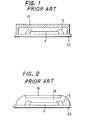
- Patent Application Laid-open Hei 11 No.296638 discloses a technique for sealing an IC chip and its peripheral parts within a concave housing while leaving a hollow therein.
- the sectional structure of a module of this technique is shown in Fig.1.
- the module shown in this drawing has an IC chip 4 provided on a printed wiring board 20 while electrodes of IC chip 4 are electrically connected to predetermined terminals of printed wiring board 20 by wires 5, and then covered by a concave housing 17 so as to isolate and protect IC chip 4 and wires 5 from the outside air.
- a material which has a higher modulus of elasticity than that of single crystalline silicon is used for concave housing 17 so as to protect IC chip 4 and reinforce the module.
- the module is encased by joining only the interface between printed wiring board 20 and concave housing 17 while IC chip 4 and wires 5 remain within the hollow.
- the interface between printed wiring board 20 and concave housing 17 may crack and water can enter through the cracks easily.
- an organic substrate such as of glass epoxy, polyimide or the like is employed, repeated cycles of moisture absorption, reduction in ambient temperature and condensation of the interior atmosphere will cause condensation of water around IC chip 4 and its peripheral parts inside the hollowed space since the organic substrate itself easily permits moisture to penetrate therethrough.
- Japanese Patent Application Laid-open Hei 11 No.238744 discloses a sealing technique in which an IC chip 4 is encapsulated with an uncured sealing resin, covered with a disk, called a topping foil 18, which is cut out from an epoxy or polyimide resin film by a punching tool, and cured.
- the sectional module structure of this prior art is shown in Fig.2.
- the module shown in this drawing is constructed by providing an IC chip 4 on a printed wiring board 20, electrically connecting terminals of printed wiring board 20 with predetermined electrodes of IC chip 4, applying a liquid resin 19 over the chip and placing a sheet, i.e., topping foil 18, so as to secure a smooth surface.
- topping foil 18 it is possible to improve controllability of the module thickness by placing topping foil 18 over liquid resin 19. Further, topping foil 18 also serves as a reinforcing element and hence improves the resistance against impacts.
- the concave housing 17 is formed of a material having an extremely low permeability, if a hollow exists inside concave housing 17, moisture penetration will occur through the surface of adhesion or through printed wiring board 20, which is usually formed of glass epoxy, polyimide or other organic compounds, and the temperature in the hollow will increase.
- the module is used under an external environment of 30° C, 70%RH, the moisture inside concave housing 17 soon becomes equal to that of the external environment.
- the moisture therein condenses and causes electric leakage in the interconnection circuit on the IC chip 4 surface and in printed wiring board 20, resulting in operation errors.
- topping foil 18 is cut out by a punching tool and placed and cured to complete sealing.
- This topping foil 18 plays the role of regulating the height of the resin seal of the IC card module and provides the reinforcing function, but will not provide any contribution to protection against external environment.
- the present invention has been devised in view of what has been discussed above, it is therefore an object of the present invention to provide a semiconductor module which can prevent occurrence of defects accompanying penetration of moisture when exposed to a heavy environment such as a high temperature high humidity storage environment, a high temperature high humidity environment with a bias applied, a vapor pressurized environment or the like, which is comparable to the conditions of environment resistance tests on IC modules and which can reduce occurrence of defects in actual environment resistance tests and hence improve the production yield as well as improving the reliability under practical usage environments. That is, the object of the present invention is to provide such a semiconductor module and its production method and a module for IC cards and the like.
- the present invention is configured as follows:
- a semiconductor module comprises: a printed wiring board made of an insulator with conductor patterns formed on both sides thereof; and a semiconductor chip mounted on the printed wiring board and sealed with a resin, and is characterized in that a metallic sheet or moisture penetration blocking sheet is adhered on the semiconductor chip surface opposite to the side that faces the printed wiring board.
- the semiconductor module having the above first feature further comprises antenna connection terminals provided on the printed wiring board surface on which the semiconductor chip is provided and/or electric connection electrodes provided on the underside opposite to the surface on which the semiconductor chip is mounted.
- the semiconductor module having the above first feature is characterized in that the metallic sheet is formed of stainless steel, 42 alloy, aluminum or copper.
- the semiconductor module having the above first feature is characterized in that moisture penetration blocking sheet is formed of alumina ceramics.
- the semiconductor having the above first feature is characterized in that the thickness of the metallic sheet or moisture penetration blocking sheet is 100 ⁇ m or below.
- the semiconductor module having the above first feature is characterized in that an adhesive layer is provided for bonding the semiconductor chip and the metallic sheet or the moisture penetration blocking sheet and the thickness of the adhesive layer is 30 ⁇ m or below.
- the semiconductor module having the above first feature is characterized in that the non-adhering surface of the metallic sheet is formed with indentations and projections.
- a semiconductor module production method whereby a semiconductor chip is mounted on a printed wiring board made of an insulator with conductor patterns formed on both sides thereof and the printed wiring board having the semiconductor chip mounted thereon is sealed with a resin, comprises the steps of: mounting the semiconductor chip on the printed wiring board; implementing electric connection between these by wires; and adhering a metallic sheet or moisture penetration blocking sheet over the semiconductor chip surface with an adhesive layer therebetween before sealing with a mold resin over the semiconductor chip mounted side of the printed wiring board.
- a semiconductor module production method whereby a semiconductor chip is mounted on a printed wiring board made of an insulator with conductor patterns formed on both sides thereof and the printed wiring board having the semiconductor chip mounted thereon is sealed with a resin, comprises the step of: forming indentations and projections on one side of the metallic sheet or moisture penetration blocking sheet which is adhered to the semiconductor chip surface before sealing with a mold resin over the semiconductor chip mounted side of the printed wiring board.
- the semiconductor module production method having the above eighth feature is characterized in that electric connection with wires between the printed wiring board and the semiconductor chip is implemented by normal wire bonding or by joining wires by ball bonding to the electrodes of the semiconductor chip first and then joining them by stitch bonding to the predetermined terminals on the printed wiring board.
- the semiconductor module production method having the above ninth feature is characterized in that electric connection with wires between the printed wiring board and the semiconductor chip is implemented by normal wire bonding or by joining wires by ball bonding to the electrodes of the semiconductor chip first and then joining them by stitch bonding to the predetermined terminals on the printed wiring board.
- the semiconductor module production method having the above eighth feature is characterized in that electric connection with wires between the printed wiring board and the semiconductor chip is implemented by reverse wire bonding or by joining wires by ball bonding to the predetermined terminals of the printed wiring board first and then joining them by stitch bonding to the electrodes of the semiconductor chip.
- the semiconductor module production method having the above ninth feature is characterized in that electric connection with wires between the printed wiring board and the semiconductor chip is implemented by reverse wire bonding or by joining wires by ball bonding to the predetermined terminals of the printed wiring board first and then joining them by stitch bonding to the electrodes of the semiconductor chip.
- a module for IC cards and the like includes a semiconductor module, comprising: a printed wiring board made of an insulator with conductor patterns formed on both sides thereof; and, a semiconductor chip mounted on the printed wiring board and sealed with a resin, wherein a metallic sheet or moisture penetration blocking sheet is adhered on the semiconductor chip surface opposite to the side that faces the printed wiring board.
- the module for IC cards and the like may be of a non-contact type, contact type or combination type having both the contact type and non-contact type functions.
- the module for IC cards and the like is mainly used for IC card modules but should not be limited to this and can be applied for other purposes.
- a double-sided printed wiring board 20 is comprised of an insulating layer 8 for polyimide double-sided interconnections, made up of glass epoxy impregnated with epoxy resin, having a thickness of 50 to 100 ⁇ m and a conductor which can be patterned by etching or other processes (forming aftermentioned antenna connection terminals 7 for the module and predetermined terminals 11 of printed wiring board 20) such as copper foil or the like, adhered on both sides of the insulator.
- This conductor is specified to have a thickness of 8 to 20 ⁇ m.
- a glass epoxy substrate having conductor layers of 12 ⁇ m thick on both sides thereof is shown as an example, but the conductor should not be limited particularly as long as it falls within the above range.
- Printed wiring board 20 has through-holes 9 drilled for electric connection between the conductor layers on both sides and has conductor layers of 10 ⁇ m thick formed on both sides by plating. The thus formed conductor layers are patterned by etching or the like to complete a printed wiring board 20.
- the printed wiring board 20 shown in the present embodiment has an insulating layer 8 of 80 ⁇ m thick.
- IC chips 4 handled in a typical wafer fabrication process have a thickness of 400 to 700 ⁇ m, but for an IC card module 16 shown in Fig.9, the undersurface of a wafer is ground so that a resultant IC chip 4 has a thickness of 50 to 200 ⁇ m.
- a film adhesive 10 of 10 to 50 ⁇ m thick is applied beforehand on the underside of the wafer. The wafer is cut by a diamond blade or the like into chips so that each IC chip 4 with adhesive 10 is mounted to printed wiring board 20.
- Adhesive 10 may use thermosetting resin, thermoplastic resin or mixture of thermosetting and thermoplastic resins and is applied under the necessary temperature and pressure.
- Adhesive 10 for IC chip 4 may be applied beforehand at the predetermined position on printed wiring board 20.
- the adhesive 10 for IC chip 4 here is specified to be 30 ⁇ m thick.
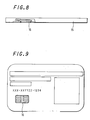
- Fig.8 is a structural sectional view showing a semiconductor module 16 of the present invention, embedded in an IC card substrate 15 and Fig.9 is a plan view showing the IC card illustrated in Fig.8.
- predetermined electrodes of IC chip 4 are connected to the predetermined terminals 11 on printed wiring board 20 by extra fine aluminum or gold wires having a diameter of 20 to 30 ⁇ m.
- Fig.3 shows a configuration in which wire bonding using gold wire 5 is performed by a method generally called normal bonding. In this process, gold wire 5 is connected first at a predetermined electrode of IC chip 4, then the other end of wire 5 is joined to the associated terminal 11 on printed wiring board 20. When gold wire 5 is used, gold balls are formed in advance on the predetermined electrodes on IC chip 4.
- a sheet 2 having a thickness equal to or smaller than 100 ⁇ m is applied over the surface of IC chip 4 with an adhesive 3 having a thickness of 50 ⁇ m or smaller, before the mounted face of IC chip 4 is sealed with a mold resin as designated at a reference numeral 1.
- This sheet 2 may be formed of stainless steel, 42 alloy, aluminum, copper or other metal sheets, or may be a moisture penetration blocking sheet made of alumina ceramics providing the inhibition against moisture penetration.
- the thickness of sheet 2 is set at 80 ⁇ m and the thickness of adhesive 3 is set at 30 ⁇ m.
- Fig. 5 the resin sealed surface of sheet 2 is formed with indentations and projections by etching, machining or other processes.
- Other configurations are the same as the above embodiment so that description is omitted.
- provision of continual indentations and projections makes it possible to markedly improve the strength of adherence.
- sheet 2 for inhibiting moisture penetration is applied in tight contact with the top surface of IC chip 4 on which active circuitry is formed, it is possible to block moisture permeating through the bulk of epoxy resin 1 as the sealing resin, in a markedly effective manner.
- application of sheet 2 of 50 ⁇ m or smaller in thickness, which is made of stainless steel, 42 alloy, aluminum, copper or alumina ceramics totally shuts out moisture permeation, over IC chip 4 with adhesive 3, isolate IC chip 4 from epoxy resin 1, whereby no condensation of permeating moisture through epoxy resin 1 will occur over the interface of IC chip 4.
- the module of the present invention has a more effective structure capable of providing an improved confidentiality compared to the configuration where the IC chip 4 surface is sealed with epoxy resin 1 only because the internal structure, or the circuitry forming face on the IC chip 4 surface cannot be viewed even if epoxy resin 1 is unsealed with a chemical having resin dissolving capability, such as hot concentrated sulfuric acid, fuming nitric acid and the like.
- the circuit of IC chip 4 is generally formed on a silicon substrate, the sheet 2 for inhibiting moisture from penetrating from the outside can also be expected to provide a reinforcing function of improving strength against bending of the thinned IC chip 4.
- the IC card modules 16 shown in Figs .3 to 5 are provided with a tuning capacitor 6.
- This tuning capacitor 6 in cooperation with an antenna connected via antenna terminals 7, constitutes a tuning circuit for non-contact communication, and is used when the module is applied as a non-contact type IC card. If the module is dedicatedly used for contact type IC cards, this can be omitted.
- IC card module 16 can be completed, but it is necessary for a non-contact type IC card or combination type IC card for non-contact and contact types, to have an external communication antenna formed with the connection terminals.
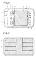
- Fig. 6 is a plan view showing the structure of a combination type IC card module 16 which has a tuning chip capacitor 6 with external terminals, mounted within the common resin sealed area. That is, the structure shown in Fig.6 includes terminals for connection to an antenna for non-contact communication and tuning capacitor, and further has four sets of electrodes 14 for contact communication formed on the underside thereof, as shown in Fig.7.
- sheet 2 is applied on IC chip 4 with adhesive 3, and wire terminals 13 of IC chip 4 and wire terminals 12 of printed wiring board 20 including insulating layer 8 are bonded by wires 5.
- the whole structure is sealed with epoxy resin 1 so as to cover tuning capacitor 6. Further, transmission/reception antenna connection terminals 7 are provided on printed wiring board 20.
- the thickness of each part of the finished IC card module 16 of this embodiment is attained as follows.
- IC chip 4 is 80 ⁇ m thick
- adhesive 10 for IC chip 4 is 30 ⁇ m thick
- sheet 2 is 80 ⁇ m thick.
- the thicknesses are as follows:
- the total thickness 344 ⁇ m.
- the thus obtained IC card module 16 of the present invention is able to avoid operation failures due to moisture penetration when it is exposed to a severe environment such as a high temperature high humidity storage environment (60°C 90%RH, or 85°C85%RH), a high temperature high humidity storage environment with a bias (a voltage double that of the maximum rating is applied for bias test under a 60°C 90%RH or 85°C 85%RH environment) applied, or a vapor pressurized environment (121°C, 2 atm. and 100%RH). Accordingly, it is possible to reduce the occurrence of defects in environmental tests on IC card modules 16 and improve the production yield as well as improving the reliability under usage environments.
- a severe environment such as a high temperature high humidity storage environment (60°C 90%RH, or 85°C85%RH)
- a bias a voltage double that of the maximum rating is applied for bias test under a 60°C 90%RH or 85°C 85%RH environment
- a vapor pressurized environment 121°C, 2 atm.
- the finished IC card module 16 is tested as to electric characteristics of IC chip 4.
- a sheet 2 that blocks moisture penetration to the IC chip 4 surface of IC card module 16 is applied with adhesive 3 of a small thickness and epoxy resin 1 is injected to the assembly by the transfer molding process. Therefore, it is possible to create a strongly-built module configuration and provide a structure of IC card module 16 having excellent resistance against extreme environments. Since the components are fabricated with the above specified thicknesses, the IC card having this IC card module 16 can be further improved in portability and can be provided in an ultrathin configuration.
- the IC card module of the present invention is able to eliminate operation failures due to moisture penetration against severe environments comparable to environment resistance tests, such as a high temperature high humidity storage environment (60°C 90%RH, or 85°C85%RH), a high temperature high humidity storage environment with a bias (a voltage double that of the maximum rating is applied for bias test under a 60°C90%RH or 85°C 85%RH environment), or a vapor pressurized environment(121°C, 2 atm. and 100%RH).
- a high temperature high humidity storage environment 60°C 90%RH, or 85°C85%RH
- a high temperature high humidity storage environment with a bias a voltage double that of the maximum rating is applied for bias test under a 60°C90%RH or 85°C 85%RH environment
- a vapor pressurized environment 121°C, 2 atm. and 100%RH.
- sheet 2 provides the reinforcing function for making up for the reduction in strength against bending accompanying the thinning of IC chip 4 mounted on the module, this configuration is able to maintain the mechanical strength in a markedly efficient manner even if, for example, the module is developed into a thin configuration.
- the sheet 2 will not be easily dissolved even if sealing epoxy resin 1 is unsealed with chemicals such as hot concentrated sulfuric acid, fuming nitric acid or the like and will be able to provide the function of a blocking layer which is resistant to chemicals. Therefore, the surface circuit structure on the IC chip 4 of the module cannot be viewed easily, so that this configuration is expected to provide remarkable security protection. Resultantly, the module of the present invention can be expected to provide unlimited effect even if it is applied to IC cards of which security is especially important.
- the present invention it is possible to prevent occurrence of defects accompanying moisture penetration even under a severe environment such as a high temperature high humidity storage environment, high temperature high humidity environments with a bias applied, a vapor pressurized environment and the like, which are the requirements imposed by the environment resistance test of the IC card module. Further, achievement of the above effect makes it possible to reduce the occurrence of defects in the actual environment resistance test based on the aforementioned conditions and hence improve the production yield as well as improving the reliability under practical usage environments.
Landscapes
- Structures Or Materials For Encapsulating Or Coating Semiconductor Devices Or Solid State Devices (AREA)
- Credit Cards Or The Like (AREA)
- Wire Bonding (AREA)
- Encapsulation Of And Coatings For Semiconductor Or Solid State Devices (AREA)
- Non-Metallic Protective Coatings For Printed Circuits (AREA)
Abstract
Description
Claims (15)
- A semiconductor module, comprising:characterized in that a metallic sheet or moisture penetration blocking sheet is adhered on the semiconductor chip surface opposite to the side that faces the printed wiring board.a printed wiring board made of an insulator with conductor patterns formed on both sides thereof; and,a semiconductor chip mounted on the printed wiring board and sealed with a resin,
- The semiconductor module according to Claim 1, further comprising antenna connection terminals provided on the printed wiring board surface on which the semiconductor chip is provided and/or electric connection electrodes provided on the underside opposite to the surface on which the semiconductor chip is mounted.
- The semiconductor module according to Claim 1, wherein the metallic sheet is formed of stainless steel, 42 alloy, aluminum or copper.
- The semiconductor module according to Claim 1, wherein moisture penetration blocking sheet is formed of alumina ceramics.
- The semiconductor module according to Claim 1, wherein the thickness of the metallic sheet or moisture penetration blocking sheet is 100 µm or below.
- The semiconductor module according to Claim 1, wherein an adhesive layer is provided for bonding the semiconductor chip and the metallic sheet or the moisture penetration blocking sheet and the thickness of the adhesive layer is 30 µm or below.
- The semiconductor module according to Claim 1, wherein the non-adhering surface of the metallic sheet is formed with indentations and projections.
- A semiconductor module production method whereby a semiconductor chip is mounted on a printed wiring board made of an insulator with conductor patterns formed on both sides thereof and the printed wiring board having the semiconductor chip mounted thereon is sealed with a resin, the method comprising the steps of:mounting the semiconductor chip on the printed wiring board;implementing electric connection between these by wires; andadhering a metallic sheet or moisture penetration blocking sheet over the semiconductor chip surface with an adhesive layer therebetween before sealing with a mold resin over the semiconductor chip mounted side of the printed wiring board.
- A semiconductor module production method whereby a semiconductor chip is mounted on a printed wiring board made of an insulator with conductor patterns formed on both sides thereof and the printed wiring board having the semiconductor chip mounted thereon is sealed with a resin, the method comprising the step of:forming indentations and projections on one side of a metallic sheet or moisture penetration blocking sheet which is adhered to the semiconductor chip surface before sealing with a mold resin over the semiconductor chip mounted side of the printed wiring board.
- The semiconductor module production method according to Claim 8, wherein electric connection with wires between the printed wiring board and the semiconductor chip is implemented by normal wire bonding or by joining wires by ball bonding to the electrodes of the semiconductor chip first and then joining them by stitch bonding to the predetermined terminals on the printed wiring board.
- The semiconductor module production method according to Claim 9, wherein electric connection with wires between the printed wiring board and the semiconductor chip is implemented by normal wire bonding or by joining wires by ball bonding to the electrodes of the semiconductor chip first and then joining them by stitch bonding to the predetermined terminals on the printed wiring board.
- The semiconductor module production method according to Claim 8, wherein electric connection with wires between the printed wiring board and the semiconductor chip is implemented by reverse wire bonding or by joining wires by ball bonding to the predetermined terminals of the printed wiring board first and then joining them by stitch bonding to the electrodes of the semiconductor chip.
- The semiconductor module production method according to Claim 9, wherein electric connection with wires between the printed wiring board and the semiconductor chip is implemented by reverse wire bonding or by joining wires by ball bonding to the predetermined terminals of the printed wiring board first and then joining them by stitch bonding to the electrodes of the semiconductor chip.
- A module for IC cards and the like, including a semiconductor module, comprising: a printed wiring board made of an insulator with conductor patterns formed on both sides thereof; and, a semiconductor chip mounted on the printed wiring board and sealed with a resin, wherein a metallic sheet or moisture penetration blocking sheet is adhered on the semiconductor chip surface opposite to the side that faces the printed wiring board.
- A semiconductor module, comprising:characterised in that a protective sheet is affixed on the semiconductor chip surface opposite said side thereof that faces the wiring board.a wiring board having an insulating layer and a conductor pattern formed thereon; anda semiconductor chip mounted on the wiring board with one side thereof facing a side of the wiring board bearing said conductor pattern, said semiconductor chip being sealed with a resin;
Applications Claiming Priority (2)
| Application Number | Priority Date | Filing Date | Title |
|---|---|---|---|
| JP2001368945 | 2001-12-03 | ||
| JP2001368945A JP3907461B2 (en) | 2001-12-03 | 2001-12-03 | Manufacturing method of semiconductor module |
Publications (2)
| Publication Number | Publication Date |
|---|---|
| EP1321979A2 true EP1321979A2 (en) | 2003-06-25 |
| EP1321979A3 EP1321979A3 (en) | 2005-10-12 |
Family
ID=19178435
Family Applications (1)
| Application Number | Title | Priority Date | Filing Date |
|---|---|---|---|
| EP02257616A Ceased EP1321979A3 (en) | 2001-12-03 | 2002-11-04 | Semiconductor module with increased reliability against heavy environment conditions and production method therefor |
Country Status (6)
| Country | Link |
|---|---|
| US (1) | US7135782B2 (en) |
| EP (1) | EP1321979A3 (en) |
| JP (1) | JP3907461B2 (en) |
| KR (1) | KR20030045612A (en) |
| CN (1) | CN1266763C (en) |
| TW (1) | TWI301588B (en) |
Families Citing this family (34)
| Publication number | Priority date | Publication date | Assignee | Title |
|---|---|---|---|---|
| US6919646B2 (en) * | 2002-03-12 | 2005-07-19 | Nec Electronics Corporation | Semiconductor device with contacting electrodes |
| EP1563570A1 (en) | 2002-11-07 | 2005-08-17 | Fractus, S.A. | Integrated circuit package including miniature antenna |
| EP1594163A1 (en) * | 2004-05-03 | 2005-11-09 | Commissariat A L'energie Atomique | A screened electrical device and a process for manufacturing the same |
| JP2005332158A (en) * | 2004-05-19 | 2005-12-02 | Kyodo Printing Co Ltd | IC module and IC card |
| EP1771919A1 (en) * | 2004-07-23 | 2007-04-11 | Fractus, S.A. | Antenna in package with reduced electromagnetic interaction with on chip elements |
| JP2007004775A (en) * | 2005-05-23 | 2007-01-11 | Toshiba Corp | Semiconductor memory card |
| JP4610613B2 (en) * | 2005-05-24 | 2011-01-12 | 富士通株式会社 | IC tag mounting structure and IC chip for mounting |
| JP2007073849A (en) * | 2005-09-08 | 2007-03-22 | Sharp Corp | Electronic circuit module and manufacturing method thereof |
| US8196829B2 (en) * | 2006-06-23 | 2012-06-12 | Fractus, S.A. | Chip module, sim card, wireless device and wireless communication method |
| JP2008171927A (en) * | 2007-01-10 | 2008-07-24 | Renesas Technology Corp | Semiconductor device |
| US8018064B2 (en) * | 2007-05-31 | 2011-09-13 | Infineon Technologies Ag | Arrangement including a semiconductor device and a connecting element |
| US20090115070A1 (en) * | 2007-09-20 | 2009-05-07 | Junji Tanaka | Semiconductor device and method for manufacturing thereof |
| DE102008031231B4 (en) * | 2008-07-02 | 2012-12-27 | Siemens Aktiengesellschaft | Manufacturing process for planar electronic power electronics modules for high-temperature applications and corresponding power electronics module |
| CN102171816B (en) * | 2008-10-03 | 2013-09-25 | 松下电器产业株式会社 | Wiring board, semiconductor device and manufacturing method thereof |
| US8424176B2 (en) * | 2008-11-25 | 2013-04-23 | Kovio, Inc. | Methods of forming tunable capacitors |
| CN101847591B (en) * | 2009-03-27 | 2012-03-21 | 王海泉 | Method for packaging multiple chips on strip |
| TWI401773B (en) * | 2010-05-14 | 2013-07-11 | 南茂科技股份有限公司 | Chip packaging device and method of manufacturing same |
| US8917511B2 (en) * | 2010-06-30 | 2014-12-23 | Panasonic Corporation | Wireless power transfer system and power transmitting/receiving device with heat dissipation structure |
| CN102655715B (en) * | 2011-03-02 | 2016-05-11 | 三星半导体(中国)研究开发有限公司 | Flexible printed circuit board and manufacture method thereof |
| US8649820B2 (en) | 2011-11-07 | 2014-02-11 | Blackberry Limited | Universal integrated circuit card apparatus and related methods |
| JP6048910B2 (en) * | 2011-11-14 | 2016-12-21 | 住友電気工業株式会社 | Reactor, coil molded body, converter, and power converter |
| USD703208S1 (en) | 2012-04-13 | 2014-04-22 | Blackberry Limited | UICC apparatus |
| US8936199B2 (en) | 2012-04-13 | 2015-01-20 | Blackberry Limited | UICC apparatus and related methods |
| USD701864S1 (en) * | 2012-04-23 | 2014-04-01 | Blackberry Limited | UICC apparatus |
| JP5951361B2 (en) * | 2012-05-31 | 2016-07-13 | 株式会社東芝 | Wireless communication device |
| DE102013205138A1 (en) * | 2013-03-22 | 2014-09-25 | Infineon Technologies Ag | Semiconductor device, semiconductor module and method for producing a semiconductor device and a semiconductor module |
| JP6119664B2 (en) * | 2014-05-14 | 2017-04-26 | 株式会社オートネットワーク技術研究所 | Circuit assembly and electrical junction box |
| CN105280572A (en) * | 2014-06-05 | 2016-01-27 | 东琳精密股份有限公司 | Package structure of thinned chip and manufacturing method thereof |
| TWI591707B (en) * | 2014-06-05 | 2017-07-11 | 東琳精密股份有限公司 | Package structure of thinned wafer and manufacturing method thereof |
| DE102015102453A1 (en) * | 2015-02-20 | 2016-08-25 | Heraeus Deutschland GmbH & Co. KG | Ribbon-shaped substrate for the production of chip card modules, chip card module, electronic device with such a chip card module and method for producing a substrate |
| US9721812B2 (en) * | 2015-11-20 | 2017-08-01 | International Business Machines Corporation | Optical device with precoated underfill |
| DE102016106698A1 (en) * | 2016-04-12 | 2017-10-12 | Infineon Technologies Ag | Chip card and method for producing a chip card |
| CN110600496A (en) * | 2019-09-20 | 2019-12-20 | 上海显耀显示科技有限公司 | Micro-LED chip packaging structure |
| KR102345062B1 (en) * | 2019-11-20 | 2021-12-30 | (주)에이티세미콘 | Semiconductor package and manufacturing method thereof |
Family Cites Families (34)
| Publication number | Priority date | Publication date | Assignee | Title |
|---|---|---|---|---|
| JPS6076040A (en) | 1983-09-30 | 1985-04-30 | Nec Home Electronics Ltd | Objective lens supporter |
| JPS60186985A (en) * | 1984-03-06 | 1985-09-24 | Toshiba Corp | Ic card |
| JPS61159746A (en) * | 1985-01-08 | 1986-07-19 | Kyodo Printing Co Ltd | Wire bonding method for ic module |
| JPS61169746A (en) | 1985-01-23 | 1986-07-31 | Sumitomo Metal Ind Ltd | Infrared ray type water measuring apparatus |
| US5175612A (en) * | 1989-12-19 | 1992-12-29 | Lsi Logic Corporation | Heat sink for semiconductor device assembly |
| JPH04280459A (en) * | 1991-03-08 | 1992-10-06 | Matsushita Electron Corp | Semiconductor device sealed with resin |
| US5311059A (en) * | 1992-01-24 | 1994-05-10 | Motorola, Inc. | Backplane grounding for flip-chip integrated circuit |
| US5612576A (en) * | 1992-10-13 | 1997-03-18 | Motorola | Self-opening vent hole in an overmolded semiconductor device |
| JPH06163755A (en) | 1992-11-24 | 1994-06-10 | Mitsubishi Electric Corp | Resin-sealed semiconductor device |
| US5430331A (en) * | 1993-06-23 | 1995-07-04 | Vlsi Technology, Inc. | Plastic encapsulated integrated circuit package having an embedded thermal dissipator |
| KR970005712B1 (en) * | 1994-01-11 | 1997-04-19 | 삼성전자 주식회사 | High heat sink package |
| JPH07288263A (en) * | 1994-04-19 | 1995-10-31 | Nitto Denko Corp | Method of manufacturing semiconductor device and metal foil material |
| US5969414A (en) * | 1994-05-25 | 1999-10-19 | Advanced Technology Interconnect Incorporated | Semiconductor package with molded plastic body |
| US5972736A (en) * | 1994-12-21 | 1999-10-26 | Sun Microsystems, Inc. | Integrated circuit package and method |
| KR0119757Y1 (en) * | 1994-12-27 | 1998-07-01 | 문정환 | Semiconductor package |
| US5786738A (en) * | 1995-05-31 | 1998-07-28 | Fujitsu Limited | Surface acoustic wave filter duplexer comprising a multi-layer package and phase matching patterns |
| JP3210835B2 (en) * | 1995-06-07 | 2001-09-25 | 京セラ株式会社 | Package for storing semiconductor elements |
| US5705851A (en) * | 1995-06-28 | 1998-01-06 | National Semiconductor Corporation | Thermal ball lead integrated package |
| JP3825475B2 (en) * | 1995-06-30 | 2006-09-27 | 株式会社 東芝 | Manufacturing method of electronic parts |
| JP3007833B2 (en) | 1995-12-12 | 2000-02-07 | 富士通株式会社 | Semiconductor device and its manufacturing method, lead frame and its manufacturing method |
| US5736785A (en) * | 1996-12-20 | 1998-04-07 | Industrial Technology Research Institute | Semiconductor package for improving the capability of spreading heat |
| JPH11102985A (en) * | 1997-09-26 | 1999-04-13 | Mitsubishi Electric Corp | Semiconductor integrated circuit device |
| JPH11238744A (en) * | 1998-02-20 | 1999-08-31 | Toppan Printing Co Ltd | Sealing method of IC module for IC card etc. |
| JPH11296638A (en) * | 1998-04-10 | 1999-10-29 | Nippon Telegr & Teleph Corp <Ntt> | IC card |
| JP4215886B2 (en) | 1999-02-03 | 2009-01-28 | ソニー株式会社 | Semiconductor integrated circuit chip sealing method and semiconductor integrated circuit card manufacturing method |
| JP2000155822A (en) * | 1998-11-19 | 2000-06-06 | Toppan Printing Co Ltd | Non-contact type IC card |
| TW411595B (en) * | 1999-03-20 | 2000-11-11 | Siliconware Precision Industries Co Ltd | Heat structure for semiconductor package device |
| JP4649688B2 (en) * | 1999-04-28 | 2011-03-16 | 凸版印刷株式会社 | Non-contact IC card |
| JP2001109860A (en) | 1999-10-05 | 2001-04-20 | Toshiba Chem Corp | Data carrier and its manufacturing method |
| FR2799883B1 (en) * | 1999-10-15 | 2003-05-30 | Thomson Csf | METHOD OF ENCAPSULATING ELECTRONIC COMPONENTS |
| TW452956B (en) * | 2000-01-04 | 2001-09-01 | Siliconware Precision Industries Co Ltd | Heat dissipation structure of BGA semiconductor package |
| US6559525B2 (en) * | 2000-01-13 | 2003-05-06 | Siliconware Precision Industries Co., Ltd. | Semiconductor package having heat sink at the outer surface |
| KR100522838B1 (en) * | 2000-10-23 | 2005-10-19 | 앰코 테크놀로지 코리아 주식회사 | Semiconductor package and method for manufacturing the same |
| US6734552B2 (en) * | 2001-07-11 | 2004-05-11 | Asat Limited | Enhanced thermal dissipation integrated circuit package |
-
2001
- 2001-12-03 JP JP2001368945A patent/JP3907461B2/en not_active Expired - Fee Related
-
2002
- 2002-11-04 EP EP02257616A patent/EP1321979A3/en not_active Ceased
- 2002-11-07 US US10/289,395 patent/US7135782B2/en not_active Expired - Fee Related
- 2002-11-29 TW TW091134771A patent/TWI301588B/en not_active IP Right Cessation
- 2002-12-02 KR KR1020020075789A patent/KR20030045612A/en not_active Ceased
- 2002-12-03 CN CNB021540020A patent/CN1266763C/en not_active Expired - Fee Related
Also Published As
| Publication number | Publication date |
|---|---|
| US7135782B2 (en) | 2006-11-14 |
| TW200301871A (en) | 2003-07-16 |
| JP2003168768A (en) | 2003-06-13 |
| CN1423315A (en) | 2003-06-11 |
| US20030102544A1 (en) | 2003-06-05 |
| CN1266763C (en) | 2006-07-26 |
| KR20030045612A (en) | 2003-06-11 |
| JP3907461B2 (en) | 2007-04-18 |
| EP1321979A3 (en) | 2005-10-12 |
| TWI301588B (en) | 2008-10-01 |
Similar Documents
| Publication | Publication Date | Title |
|---|---|---|
| US7135782B2 (en) | Semiconductor module and production method therefor and module for IC cards and the like | |
| JP4753170B2 (en) | Semiconductor device and manufacturing method thereof | |
| US6422473B1 (en) | Circuit chip mounted card and circuit chip module | |
| US6633078B2 (en) | Semiconductor device, method for manufacturing an electronic equipment, electronic equipment and portable information terminal | |
| US7193161B1 (en) | SiP module with a single sided lid | |
| US7939935B2 (en) | Electronic device substrate, electronic device and methods for fabricating the same | |
| US6518885B1 (en) | Ultra-thin outline package for integrated circuit | |
| US6208019B1 (en) | Ultra-thin card-type semiconductor device having an embredded semiconductor element in a space provided therein | |
| JP4379102B2 (en) | Manufacturing method of semiconductor device | |
| KR20030051276A (en) | Semiconductor device and fabrication method thereof | |
| US20100013076A1 (en) | Semiconductor device package and method of fabricating the same | |
| JP3449796B2 (en) | Method for manufacturing resin-encapsulated semiconductor device | |
| KR20020084889A (en) | Semiconductor device | |
| US6337225B1 (en) | Method of making stacked die assemblies and modules | |
| JP2003092375A (en) | Semiconductor device, its manufacturing method and its inspection method | |
| JP2010199625A (en) | Semiconductor device, and method of manufacturing the same | |
| US10176420B2 (en) | Strip-type substrate for producing chip card modules | |
| US20260090472A1 (en) | Method of manufacturing a semiconductor package | |
| KR100592785B1 (en) | Stacked package with chip scale packages | |
| JP2007188489A (en) | Smart card module | |
| KR100385088B1 (en) | Multi-chip semiconductor module and manufacturing process thereof | |
| JPH11316811A (en) | Data carrier equipment | |
| JP2884837B2 (en) | Semiconductor device | |
| JP2007213463A (en) | Non-contact data carrier, wiring board for non-contact data carrier | |
| JPH02293197A (en) | Ic module |
Legal Events
| Date | Code | Title | Description |
|---|---|---|---|
| PUAI | Public reference made under article 153(3) epc to a published international application that has entered the european phase |
Free format text: ORIGINAL CODE: 0009012 |
|
| AK | Designated contracting states |
Designated state(s): AT BE BG CH CY CZ DE DK EE ES FI FR GB GR IE IT LI LU MC NL PT SE SK TR |
|
| AX | Request for extension of the european patent |
Extension state: AL LT LV MK RO SI |
|
| PUAL | Search report despatched |
Free format text: ORIGINAL CODE: 0009013 |
|
| AK | Designated contracting states |
Kind code of ref document: A3 Designated state(s): AT BE BG CH CY CZ DE DK EE ES FI FR GB GR IE IT LI LU MC NL PT SE SK TR |
|
| AX | Request for extension of the european patent |
Extension state: AL LT LV MK RO SI |
|
| 17P | Request for examination filed |
Effective date: 20060227 |
|
| AKX | Designation fees paid |
Designated state(s): DE FR GB |
|
| 17Q | First examination report despatched |
Effective date: 20060619 |
|
| STAA | Information on the status of an ep patent application or granted ep patent |
Free format text: STATUS: THE APPLICATION HAS BEEN REFUSED |
|
| 18R | Application refused |
Effective date: 20090614 |