EP1314198B1 - Repere de superposition, procedes servant a concevoir des reperes de superposition et procedes de mesure de superposition - Google Patents
Repere de superposition, procedes servant a concevoir des reperes de superposition et procedes de mesure de superposition Download PDFInfo
- Publication number
- EP1314198B1 EP1314198B1 EP01971384.1A EP01971384A EP1314198B1 EP 1314198 B1 EP1314198 B1 EP 1314198B1 EP 01971384 A EP01971384 A EP 01971384A EP 1314198 B1 EP1314198 B1 EP 1314198B1
- Authority
- EP
- European Patent Office
- Prior art keywords
- layer
- overlay
- working zones
- working
- mark
- Prior art date
- Legal status (The legal status is an assumption and is not a legal conclusion. Google has not performed a legal analysis and makes no representation as to the accuracy of the status listed.)
- Expired - Lifetime
Links
Images


Classifications
-
- G—PHYSICS
- G03—PHOTOGRAPHY; CINEMATOGRAPHY; ANALOGOUS TECHNIQUES USING WAVES OTHER THAN OPTICAL WAVES; ELECTROGRAPHY; HOLOGRAPHY
- G03F—PHOTOMECHANICAL PRODUCTION OF TEXTURED OR PATTERNED SURFACES, e.g. FOR PRINTING, FOR PROCESSING OF SEMICONDUCTOR DEVICES; MATERIALS THEREFOR; ORIGINALS THEREFOR; APPARATUS SPECIALLY ADAPTED THEREFOR
- G03F7/00—Photomechanical, e.g. photolithographic, production of textured or patterned surfaces, e.g. printing surfaces; Materials therefor, e.g. comprising photoresists; Apparatus specially adapted therefor
- G03F7/70—Microphotolithographic exposure; Apparatus therefor
- G03F7/70483—Information management; Active and passive control; Testing; Wafer monitoring, e.g. pattern monitoring
- G03F7/70605—Workpiece metrology
- G03F7/70616—Monitoring the printed patterns
- G03F7/70633—Overlay, i.e. relative alignment between patterns printed by separate exposures in different layers, or in the same layer in multiple exposures or stitching
Definitions
- the present invention relates generally to overlay measurement techniques, which are used in semiconductor manufacturing processes. More specifically, the present invention relates to overlay marks for measuring alignment error between different layers or different patterns on the same layer of a semiconductor wafer stack.
- overlay error between successive patterned layers on a wafer is one of the most critical process control techniques used in the manufacturing of integrated circuits and devices.
- Overlay accuracy generally pertains to the determination of how accurately a first patterned layer aligns with respect to a second patterned layer disposed above or below it and to the determination of how accurately a first pattern aligns with respect to a second pattern disposed on the same layer.
- overlay measurements are performed via test patterns that are printed together with layers of the wafer. The images of these test patterns are captured via an imaging tool and an analysis algorithm is used to calculate the relative displacement of the patterns from the captured images.
- the most commonly used overlay target pattern is the "Box-in-Box” target, which includes a pair of concentric squares (or boxes) that are formed on successive layers of the wafer.
- the overlay error is generally determined by comparing the position of one square relative to another square.
- Fig. 1A is a top view of a typical "Box-in-Box" target 10.
- the target 10 includes an inner box 12 disposed within an open-centered outer box 14.
- the inner box 12 is printed on the top layer of the wafer while the outer box 14 is printed on the layer directly below the top layer of the wafer.
- the overlay error between the two boxes, along the x-axis for example is determined by calculating the locations of the edges of lines c1 and c2 of the outer box 14, and the edge locations of the lines c3 and c4 of the inner box 12, and then comparing the average separation between lines c1 and c3 with the average separation between lines c2 and c4.
- the overlay error (along the x-axis).
- the overlay error between the two boxes along the y-axis may also be determined using the above technique.
- EP-0634702-A1 discloses a method and apparatus for measuring a relative positional deviation between a first pattern and a second pattern printed on an article such as a semiconductor wafer at different times. The measurement is based on detection of interference of diffraction lights from at least one of the first and second printed patterns.
- EP-0281030-A2 discloses a method of registration measurement using overlaid test patterns by the use of reflected light.
- Two identical test patterns are overlaid upon each other on a planar substrate of a semiconductor material.
- Each pattern consists of a plurality of spaced parallel lines arranged in two sets of horizontal and two sets of vertical lines.
- the reflected light intensities from the two sets of horizontal and vertical lines are measured allowing the calculation of the horizontal and vertical overlay error from the known periodicity of the sets of lines and the measured light intensities.
- a substrate having an overlay mark as defined in claim 1.
- the present invention is illustrated by way of example, and not by way of limitation.
- the present invention uses overlay marks that are composed of periodic structures formed on each of two layers of a semiconductor wafer to provide overlay information between those two layers of the semiconductor device.
- the overlay marks are formed in specific locations on each wafer layer such that the periodic structures on one layer will be aligned with the periodic structures on the other layer when the two layers are properly aligned. Conversely, the periodic structures on each layer will be offset from each other when the two layers are not properly aligned.
- the present invention may use overlay marks that are composed of periodic structures formed on a single layer by two or more separate processes to provide alignment information between two different patterns on the same layer.
- Each of the periodic structures is composed of a plurality of structures, which increases the amount of information that may be used to measure overlay, and which may be widely modified to diminish the impact of certain processes on the overlay measurements.
- Each of these structures is composed of sub-structures that are about the same size and pitch (e.g., separation) as structures of the actual integrated circuits. By forming each of the periodic structures with sub-structures that are sized closer to the size of the actual circuits, a more accurate measurement of any alignment error in such circuits is obtained.
- the invention is particularly suitable for overlay measurement techniques that require capturing an image of the overlay mark.
- the periodic structures and sub-structures described herein are generally patterned using suitable photolithographic techniques, and the lithographic patterns are subsequently transferred to other materials and layers using established processing techniques such as etching and deposition.
- the transferred patterns constitute etched or deposited lines or vias.
- the periodic structures and sub-structures may be formations of photoresist material, recessed cavity formations, embedded trenches and/or other structures within a wafer layer.
- the structures and sub-structures formed by cavities may be cavities formed in any of the layers during the semiconductor fabrication process.
- the cavities may be formed in the photoresist layer, the dielectric material layer, or the metal layers. It should be noted that the above processes are not a limitation and that any suitable fabrication technique may be used.
- Fig. 2 is a top plan view of an overlay mark 70, in accordance with one embodiment of the present invention.
- the mark 70 is suitable for image based overlay measurement techniques.
- overlay mark 70 is shown in a configuration that results when the tested layers of a wafer are in proper alignment.
- the overlay mark 70 is generally provided to determine the relative shift between two or more successive layers of a substrate or between two or more separately generated patterns on a single layer of a substrate.
- the overlay mark may be used to determine how accurately a first layer aligns with respect to a second layer disposed above or below it or how accurately a first pattern aligns relative to a preceding or succeeding second pattern disposed on the same layer.
- overlay marks in this figure may also be used to measure two or more separately generated patterns on a single layer of a wafer.
- any convenient orientation of the mark relative to the placement of the dies on the wafer can be chosen so long as the orientation of the successive marks is the same from layer to layer or from pattern to pattern.
- the overlay mark 70 is defined by a perimeter 71.
- the perimeter 71 is typically based on metrology tool limitations and circuit design rules. For instance, the upper limits of the perimeter may be set by the field of view (FOV) of the metrology tool used to measure overlay and/or the scribe line budget.
- the FOV generally refers to the optical perimeter that defines the area available for capturing an image via the metrology tool.
- the mark is typically positioned inside the scribe line of the wafer, i.e., the scribe line is the place on the wafer where the wafer is separated into dies via sawing or dicing and thus the circuit itself is not patterned there.
- the scribe line budget therefore, generally refers to the available space allowed by the scribe line for the placement of the mark.
- the lower limits of the perimeter may be set by the minimum area needed by the metrology tool to image the mark (e.g., obtain adequate signal or measurement quality).
- the perimeter 71 should be as a large as possible so as to maximize the amount of information used for overlay measurements.
- the size and shape of the perimeter 71 may be widely varied.
- the perimeter may form shapes such as squares circles, triangles, rectangles, polygons and the like.
- the size of the perimeter, in any given direction, is generally between about 10 and about 100 microns, and more particularly between about 20 and about 50 microns.
- the perimeter 71 directly corresponds to the size and shape of the FOV 79 of the metrology tool, i.e., the FOV defines the perimeter.
- the FOV is rectangular shaped due to CCD proportions. It should be noted, however, that this is not a limitation and that the FOV may be substantially larger than the mark's perimeter 71.
- the mark's perimeter may be limited by the area on the scribe line.
- the overlay mark 70 further includes a plurality of working zones 72, which are configured to divide and substantially fill the perimeter 71 of the mark 70 (from center to edge).
- the working zones may be configured to fill the perimeter of the mark such that the combined area of the working zones is substantially equal to the total area of the mark.
- the working zones 72 represent the actual areas of the mark that are used to calculate alignment between different layers of the wafer.
- the working zones 72 typically include information relating to the two layers for which overlay measurements are made. For example, some of the working zones are positioned in one layer of the wafer (represented by solid lines) while some of the working zones are positioned in a different layer of the wafer (represented by dashed lines).
- the working zones 72 are spatially separated from one another so that they do not overlap portions of an adjacent working zone (i.e., each of the working zones represents a different area of the mark). This is typically done to ensure that each of the working zones is properly imaged by the metrology tool.
- the working zones 72 may be spatially separated by an exclusion zone 80 so that each of the working zones is distinct.
- Exclusion zones 80 are areas of the target image where either a physical target structure or a corresponding optical signal is distorted and therefore it is excluded from the overlay calculation.
- the size of the exclusion zones is typically balanced with the size of the working zones so as to provide as much information as possible for the measurement of overlay. That is, it is generally desired to have larger working zones and smaller exclusion zones. In some cases, it may be desirable to have a small amount of overlap between adjacent working zones so as to allow SEM cross sectioning to verify the accuracy of the overlay measurements.
- the geometry, including size, shape and distribution of the working zones is configured to balance out or compensate for non-uniform or asymmetrical characteristics that may occur across the mark. Asymmetries may arise from the optical aberration and illumination asymmetry in the metrology tool (tool induced shifts), as well as process induced structural features (wafer induced shifts).
- Tool induced shift generally refers to how much the apparent position of the mark moves or shifts as a result of metrology tool problems such as non -uniform illuminations and/or optical aberrations.
- Illumination generally pertains to how the light is distributed to the target.
- Aberrations generally pertain to how the light is focussed and collected.
- Non-uniformilluminations may be caused by a defect or misalignment in one of the optical components associated with transferring the light from the light source to the wafer.
- Non-uniform optical aberrations may be caused by a defect or misalignment in the objective lens of the optical system.
- aberrations may include spherical aberrations, astigmatism aberrations and coma aberrations.
- Coma aberrations may have a greater impact on TIS as a result of its asymmetrical nature across the FOV of the metrology tool,
- Wafer induced shift generally refers to how much the apparent position of the mark moves as a result of process variations such as distortions caused by chemical mechanical polishing (CMP) and sputter deposition.
- Non-uniformities, asymmetries and variations may also arise from difference between the height of the different line sets from each layer.
- the lower layer lines are sometimes visible only through the intermediate layer of the wafer since the intermediate layer material covers the lines on the lower layer.
- the upper lines are generally formed from the photoresist applied on the top of the lower layer.
- the overlay metrology tool by adjusting the size, shape and distribution of the overlay information from the two layers or patterns within the field of view of the overlay metrology tool, it is possible to diminish the impact of lithography and/or process non-uniformities, asymmetries and variations. In some cases, it may even be possible to enhance the overlay measurement.. Resist patterns are less inclined to process variation and thus they may potentially be more useful for acquisition areas of the mark.
- balancing is accomplished by selectively positioning the working zones of the same layer at different positions around the perimeter of the mark.
- the working zones may be positioned at different positions within the FOV in order to get the best possible balance between aberrations and illumination and process results that vary across the FOV.
- working zones of the same layer are positioned opposite one another so as to balance out asymmetries that may occur from the left to the right or from the top to the bottom or from the inner to the outer regions of the FOV (or vice versa).
- the optimal distribution for balancing out asymmetries is determined by performing optical simulations of tool induced shift (e.g., how much the apparent position of the mark moves as a result of tool problems such as illumination and/or aberrations).
- the optimal distribution for balancing out asymmetries is determined by performing experiments (e.g., run a sample of wafers).
- the working zones may be positioned at specific positions inside the FOV to avoid these areas.
- each of the working zones is configured to represent one of the two successive layers of the overlay mark.
- the working zones represent an equal number of first layers or patterns and second layers or patterns, i.e., for each working zone in the first layer there is a corresponding working zone in the second layer. This is typically done to balance variations, non-uniformites and/or asymmetries that may exist in the layers and/or the metrology tool.
- the number of working zones is generally based on a factor of 2, as for example, 2, 4, 8, 16 and the like. It is generally believed that by distributing the regions to more points within the field of view, the more likely they are to balance out the non-uniformities caused by illuminations, aberrations and the process.
- the size of the working zones is generally between about 2 to about 24 microns, and more particularly between about 4 to about 15 microns. In most cases, the size of the working zones is inversely proportional to the number of working zones, i.e., as the number increases, the size decreases. By way of example, the size of the working zones is generally between about 10 and about 24 microns for four working zones, between about 5 and about 12 microns for eight working zones, and between about 2.5 and about 6 microns for sixteen working zones.
- first and second layered working zones there may be cases that require an uneven number of first and second layered working zones, i.e., 4 first layered working zones and 2 second layered working zones. There may also be the case that requires an uneven number of total working zones, i.e., 2 first layered working zones and 1 second layered working zones. There may also be the case that requires unequal working zone sizes. For example, a first group of working zones may have a first size while a second group of working zones may have a second size where the second size is either smaller or larger than the first size.
- the shape of the working zones may vary according to the specific needs of each mark.
- the zones may have a square shape (as shown), an L shape, a rectangular shape, a triangular shape, a circular shape, a polygonal shape and the like.
- the shape and size of the working zones are identical. This is typically done to balance variations, non-uniformities and/or asymmetries that may exist in the layers and/or the metrology tool.
- this is not a limitation and that some or all of the working zones may have different shapes. For example, some of the working zones may have a rectangular shape while other working zones may have a square shape.
- working zones 72A and 72D are formed in one layer of the wafer while working zones 72B and 72C are formed in a different layer of the wafer (represented by solid lines).
- working zones 72A&D are angled relative to working zones 72B&C. That is, working zones 72A&D lie crosswise relative working zones 72B&C.
- working zones 72A and 72D which are disposed on the same first layer, are positioned opposite one another at a first vertical angle while working zones 72B and 72C, which are disposed on the same second layer, are positioned opposite one another at a second vertical angle.
- working zone 72A is diagonally opposed to working zone 72D
- working zone 72B is diagonally opposed to working zone 72C
- working zone 72A is spatially offset from working zone 72D
- working zone 72B is spatially offset from working zone 72D
- the center of working zone 72D is positioned below and to the right of the center of working zone 72A
- the center of working zone 72C is positioned below and to the left of the center of working zone 72B.
- these cross-positioned structures form an "X" shaped pattern.
- the working zones may be configured to fill a variety of different sized and different shaped FOVs. It is generally desirable to fill the field of view with as much information as possible for reasons of process robustness and information optimization.
- the working zones may also be configured to take on other shapes such as rectangles, triangles, parallelograms, trapezoids, regular polygons, circles and the like.
- the opposing periodic structures may be disposed on other layers.
- working zones 72B and 72C may be disposed on the first layer (dashed lines) and working zones 72A and 72D may be disposed on the second layer (solid lines).
- the working zones may only partially fill the field of view.
- the exclusion zones may be eliminated so that the working zones may be positioned next to one another along their edges (e.g., completely filling the regions and thus the FOV) or partially over one another so as to allow for line ends to overlap for cross section accuracy.
- Each of the working zones 72 contains an individual periodic structure 74, as for example, periodic structures 74A-D. As shown, each of the periodic structures 74 substantially fills the perimeter of its corresponding working zone 72. Moreover, each of the periodic structures 74 includes a plurality of coarsely segmented lines 76 that increase the amount of information that may be used for overlay measurements. In addition, by constructing marks from periodic structures, it is possible to implement a broader range of overlay measurement algorithms that maximize the benefits of higher information density in the mark. Each of the coarsely segmented lines 76 is formed by a number of sub-structures or finely segmented elements 78.
- the finely segmented elements 78 within each periodic structure are not necessarily discontinuous linear formations that are segmented at regular intervals.
- the dashed lines may represent continuous linear formations within each of the periodic structures.
- the finely segmented elements 78 within each periodic structure may take on various shapes and sizes, which include discontinuous linear formations that are segmented at regular intervals. These will be described in greater detail below.
- the geometry, i.e., linewidth and spacing, of the periodic structure is configured to find the proper balance between the image resolution of the metrology tool and the robustness of the process. For instance, in most cases, it is desirable to have a large geometry (e.g., large linewidths and spacings) so that the periodic structure may be optically resolved by the tool, and a small geometry (e.g., small linewidths and spacings) so that the process effects on the mark are minimized.
- image resolution there is a minimum size requirement that each metrology tool has for resolving the coarsely segmented lines.
- the characteristic dimensions of these structures are approximately 1 to 2 micrometer or less in order to diminish the impact of asymmetries resultant from the polishing and aluminum deposition processes.
- the width of the trench is too small, the remaining topography at the top of the aluminum layer is too small to provide optically adequate contrast and thus the mark does not provide adequate overlay information.
- the lower bound for characteristic dimensions of structures at this scale is determined by the resolution limit of the metrology tool. For example for an overlay tool with a numerical aperture (NA) of 0.9 and a mean illumination wavelength of 550 nm gives a Rayleigh resolution limit or criteria of approximately 0.4 micrometer.
- the geometry of the periodic structure is determined by experimentation. For example, several wafers may be run through a process to find a period for which the TIS variability is the smallest, i.e., measure the tool induced shift variability at multiple sites on the wafer and then select the pitch that minimizes the TIS variability and process variability.
- the period and phase of the periodic structure is configured to filter out high frequency edges.
- each of the periodic structures 74A-D has the same pitch and duty cycle. That is, each of the periodic structures 74 consist of an equal number of coarsely segmented lines 76, which are parallel and which have equal linewidths and equal spacings therebetween.
- the dimensions of the pitch, linewidths and spacings may be widely varied.
- the dimension of the pitch may be between about 1 to about 3 microns
- the dimensions of the linewidths and spacings may be between about 0.3 to about 2 microns, and more particularly between about 0.5 to about 1 micron.
- each of the periodic structures may have a different pitch or duty cycle.
- some of periodic structures may have the same pitch or duty cycle, while other periodic structures may have a different pitch or duty cycle.
- the periodic structures may have a pitch that varies across the periodic structure.
- the periodic structure may be a chirped periodic structure (e.g., smaller to larger).
- the pitch, linewidths and spacings are generally optimized according to process robustness requirements and contrast requirements of the metrology tool.
- each periodic structure 74A-D includes 5 coarsely segmented lines. In some cases, it may even be desirable to have periodic structures having a different number of lines, i.e., a first periodic structure having 5 lines and a second periodic structure having 2 lines.
- the lines of the periodic structures 74A-D are parallel to one another so as to provide position information in a single direction.
- the lines in Fig. 2 are configured for X-axis measurements since the lines are non-parallel (e.g., perpendicular or orthogonal) to the axis of measurement.
- any offset between the two successive layers in the X-direction will be present between the first set of periodic structures 74 A&D and the second set of periodic structures 74 B&C.
- the alignment between the two layers of the wafer in the X-direction may be determined by comparing the relative positions of the two groups of periodic structures.
- the positions of periodic structures 74 A and D, which are disposed on the first layer may be compared with the positions (e.g., centers of symmetry) of periodic structures 74 B and C, which are disposed on the second layer, to determine the alignment between consecutive layers in the X direction.
- the overlay alignment between layers is determined by calculating the centers of symmetry for each of the opposing zones on the same layer, and then calculating the difference between the two averaged centers of symmetry. For example, the center of symmetry for both working zones 72A and D and working zones 72B and C may be found by folding the images over, and the difference of these two centers of symmetry may determine the overlay error. If there is zero overlay, the centers of symmetry of each of the two opposing groups on the same layer should coincide with the Y axis that runs through the middle of the mark, i.e., between the left working zones and the right working zones.
- periodic structure 74A is compared to periodic structure 74B and periodic structure 74C is compared to periodic structure 74D.
- periodic structures that are above or below one another are compared, i.e., periodic structure 74A is compared to periodic structure 74C and periodic structure 74B is compared to periodic structure 74D.
- measuring overlay in the X-direction is not a limitation and that the overlay mark 70 may be rotated 90 degrees to determine the registration error between the two layers of the wafer in the Y-direction.
- two overlay marks one of which is rotated 90 degrees from the other, can be used to determine the alignment between consecutive layers in two directions, as for example in the X and Y directions.
- the second mark may be positioned at various locations relative to the first mark so long as the orientation of the first and second marks are the same layer to layer (e.g., side by side or at different locations on the wafer if space is limited).
- each set of lines on a layer of the semiconductor wafer (except for those on the first and last layers) are used in conjunction with the lines on two layers of the semiconductor wafer, the one below and the one above. This implementation works best if the first layer cannot be detected optically when below the third layer.
- the grating pairs for each pair of adjacent layers on the wafer could be in a different location on the wafer to minimize any "bleed through" interference from a third layer on the measurement for the top two layers of interest.
- finely segmented elements 78 which are used to form each of the coarsely segmented lines 76, are configured to allow the overlay mark 70 to facilitate overlay measurements that more accurately represent the degree of alignment between the wafer layers. That is, the finely segmented elements 78 serve to provide alignment information that more closely matches the alignment of the patterns of the integrated circuits that are formed on each of the two layers. The finely segmented elements 78 allow for more representative measurements, in part, due to several reasons.
- the feature size and pitch are comparable to those of the critical device features of the patterning step performed on the layers under test. That is, the dimensions of the finely segmented elements 78 are comparable to the dimensions of the circuit patterns.
- the line has a width that is approximately equal to the width of an integrated circuit interconnection line.
- circuit interconnection lines have widths that are approximately equal to or less than 0.13 um.
- the finely segmented elements of the current invention can be made to have widths as small as 0.05 - 0.2 um. However, as can be appreciated, advances in semiconductor manufacturing processes are likely to further reduce these dimensions and therefore these dimensions are by way of example and not by way of limitation.
- Wafer fabrication asymmetries are shifts in the shape and size of structures or patterns that have been formed upon a wafer layer due to further fabrication processes.
- the effects of wafer fabrication proceses on overlay marks depends on the size, spacing and density of the overlay mark structures and substructures. These shifts in shape and size affect the overlay marks such that accuracy of the overlay measurements may be deteriorated.
- An exemplary wafer fabrication technique that may cause wafer structures to gain asymmetrical profiles is the sputter deposition process.
- the sputtering process is generally used to apply a layer of material (i.e., metal) on top of an existing wafer layer.
- the source of the sputtered material a target
- the sputtered material travels at an angle from the target towards the outer perimeter of a wafer thereby resulting in asymmetrical deposition of material within recessed channels or over ridge-like protrusions.
- the unequal accumulation of deposited material between the sidewalls of a recessed channel may cause an apparent positional shift of the recessed channel towards one side of the channel.
- CMP chemical mechanical planarization
- the resulting asymmetries to overlay marks due to the fabrication processes may be reduced by forming smaller marks.
- smaller recessed channels or ridges allows less sputtered material to accumulate on the respective side surfaces, thereby resulting in a smaller asymmetrical shift in shape and size.
- CMP process marks having smaller dimensions will also be shifted to a lesser degree.
- there may be process situations, where widening the lines of the overlay marks may make them more robust to process variation, as for example, in cases of metal layers with large grain size. Refer to Lithography Process Control, by Harry J. Levinson , for further information on wafer fabrication asymmetries.
- Fig. 3 is a partial side elevation view of any one of the periodic structures 74 shown in Fig. 2 , showing an example which is not in accordance with the invention.
- the coarsely segmented lines 76 are formed by a plurality of finely segmented elements 78.
- the finely segmented elements 78 represent bars, which are symmetrically distributed relative to the center of the coarsely segmented line 76, and which having equal fine widths, w, and fine pitch, p (distance between centers), therebetween.
- the linewidth, d, of the coarsely segmented lines 76 is defined as the distance between the outer edges of the very first and the very last bar 78' and 78" of the plurality of finely segmented bars 78. In the illustrated example, there are 10 finely segmented bars.
- stepper aberrations such as coma may cause an apparent overlay error in cases where the overlay mark is finely segmented. That is, in addition to having the tendency to cause pattern placement errors, stepper coma may also have the tendency to modify the dimensions of the finely segmented elements, in particular, the first and last bars that make up the coarsely segmented line (e.g., bars 78' and 78").
- modify the dimensions it is generally meant that the first and last bars may become thinner or wider. In most cases, when one bar becomes wider the other bar becomes thinner. For example, coma may cause the last bar to become wider and the first bar to become thinner.
- a clear field In lithography, a clear field generally refers to a series of periodic structures that are surrounded by an open space (e.g., etched) and a dark field generally refers to a series of periodic structures that are surrounded by a closed space (e.g., not etched).
- the clear fields generally appear brighter and the dark fields generally appear darker.
- the clear field is a clearing between a group of finely segmented elements such as the bars of Fig. 3
- the dark field is a closed space between a group of finely segmented elements such as the bars of Fig. 3 .
- each of the working zones includes fine segmentation that comprises both a clear field and a dark field.
- some of the coarsely segmented lines have clear fields and some have dark fields.
- the balancing is done between two periodic structures of different working zones.
- at least a first working zone includes a periodic structure with fine segmentation that comprises a clear field and at least a second working zone includes a periodic structure with fine segmentation that comprises a dark field.
- the first and second working zones are opposed working zones that are on the same layer.
- Fig. 4 is a partial side elevation view of any one of the periodic structures 74 shown in Fig. 2 , in accordance with the invention.
- Fig. 4 generally corresponds to the first implementation described above.
- the coarsely segmented lines 76 are formed by a plurality of finely segmented bars 78 and at least one dark field 81.
- the coarsely segmented lines 76 are separated by a separation, S, that includes a plurality of finely segmented bars 78 and at least one clear field 82.
- S that includes a plurality of finely segmented bars 78 and at least one clear field 82.
- the geometry of the finely segmented lines, dark fields and clear fields may be widely varied. The geometry of these components generally depends on the partial coherence of illumination and coma aberrations of the optics of the stepper lens. Dual tone structures, in which both lines and spaces are partially segmented tend to represent better the pattern placement errors suffered by device structures, rather than structures comprising either one or the other.
- Figs. 5A & B are partial side elevation views of two distinct periodic structures 84 and 85, which are not in accordance with the invention.
- the periodic structures 84 and 85 represent periodic structures, which are from opposing working zones, and which are positioned in the same layer.
- periodic structure 84 may correspond to periodic structure 74A while periodic structure 85 may correspond to periodic structure 74D.
- the first periodic structure 84 includes coarsely segmented lines 76, which are formed by a plurality of finely segmented bars 78, and which are separated by clear fields 82.
- the second periodic structure 85 includes coarsely segmented lines 76, which are formed by a plurality of finely segmented bars 78, and which are separated by dark fields 81.
- the geometry of the finely segmented lines, dark fields and clear fields may be widely varied.
- the size shape (although inverse) and position of the dark fields generally corresponds to the size shape (although inverse) and position of the clear fields.
- the advantages of the X-configuration are numerous.
- the X-configuration may provide more information than the standard box-in-box target by filling the perimeter of the mark from center to edge. It may also provide more information by increasing the number of edges (e.g., coarsely segmented lines) as well as their lengths. Apart from providing more information by increasing the number of edges and their lengths, the X-configuration exhibits further advantage over the generic box-in- box target due to additional built-in symmetry. Namely, in the generic box-in-box structures there are inner and outer layers.
- the "X"-target structure is basically invariant to the layer swap (up to mirror transformation). Furthermore, the X configuration exhibits 180 degree rotational symmetry that helps to overcome anti-symmetrical coma patterns, i.e., coma will cancel out.
- Fig. 6 is a top plan view of an overlay mark 90, in accordance with an alternate example.
- the overlay mark 90 may generally correspond to the overlay mark shown in Fig. 2 .
- Overlay mark 90 contains four working zones 92A-D for determining the registration error between two wafer layers (one layer is represented by cross-hatching, the other is not).
- Each of the working zones includes a periodic structure 94 comprised by a plurality of coarsely segmented lines 96.
- the periodic structures 94A and D positioned in the first and fourth zones 92 A and D are disposed in a first layer of the wafer while periodic structures 94 B and C positioned in the second and third zones 92 B and C are disposed in a second layer of the wafer. Furthermore, periodic structures on the same layer, as for example structures 94 A and D, are in diagonally opposed positions thereby forming an overlay mark with an X configuration.
- the coarsely segmented lines are horizontally positioned and therefore they are configured to measure overlay in the Y-direction. It should be noted, however, that this is not a limitation and that the target may be rotated so as to measure overlay in the X-direction. Also in this example, the coarsely segmented lines are solid structures that are elongated and rectangular in shape. It should also be noted that this is not a limitation and that the coarsely segmented lines may be formed by a plurality of finely segmented elements, which may be produced according to the finely segmented elements described in Fig. 4 .
- each of the working zones 92, and more particularly each of the periodic structures 94 in Fig. 6 has an "L shaped" outline or shape in order to accommodate an additional structure 96 in the center of the mark 90.
- the additional structure 96 represents a standard box in box structure as described in the background of this application.
- the "X" configured mark 90 can be acquired and measured by standard box in box metrology tools and algorithms, i.e., existing equipment and software may be used.
- Fig. 7 is a top plan view of an overlay mark 100, in accordance with an alternate example.
- the overlay mark 100 may generally correspond to the overlay mark shown in Fig. 2 .
- Overlay mark 100 contains four working zones 102A-D for determining the registration error between two wafer layers (one layer is represented by cross-hatching, the other is not).
- Each of the working zones 102 includes a periodic structure 104 comprised by a plurality of coarsely segmented lines 106. In a manner similar to the "X" target of Fig.
- the periodic structures 104A and D positioned in the first and fourth zones 102 A and D are disposed in a first layer of the wafer while periodic structures 104 B and C positioned in the second and third zones 102 B and C are disposed in a second layer of the wafer. Furthermore, periodic structures on the same layer, as for example structures 104 A and D, are in diagonally opposed positions thereby forming an overlay mark with an X configuration.
- the coarsely segmented lines 106 are horizontally positioned and therefore they are configured to measure overlay in the Y-direction. It should be noted, however, that this is not a limitation and that the mark 100 may be rotated so as to measure overlay in the X-direction. Also in this example, the coarsely segmented lines are solid structures that are elongated and rectangular in shape. It should also be noted that this is not a limitation and that the coarsely segmented lines may be formed by a plurality of finely segmented elements, which may be produced according to the finely segmented elements described in Fig. 4 .
- each of the working zones 102, and more particularly each of the periodic structures 104 in Fig. 7 has a "rectangular" outline or shape in order to accommodate an additional structure 108 in the center of the mark 100.
- the additional structure 108 represents a standard box in box structure as described in the background of this application.
- the X configured mark 100 can be acquired and imaged by standard box in box overlay metrology tools and algorithms.
- the additional structure may represent other structures, as for example, a pattern recognition structure, which can be recognized and acquired by optical pattern recognition tools and algorithms. Both configurations have the advantage that no change is necessary to existing equipment and software.
- Fig. 8 is a top plan view of an overlay mark 110, in accordance with an alternate example.
- overlay mark 110 may correspond to the mark of Fig. 2 . It should be noted, however, that unlike the mark of Fig. 2 , the overlay mark 110 is configured to measure overlay in two separate directions. As such, mark 110 obviates the need to have one mark for each direction in which overlay needs to be measured. Overlay mark 110 is shown in a configuration that results when the tested layers of a wafer are in perfect alignment.
- the overlay mark 110 includes a plurality of working zones 112 for determining the registration error between two wafer layers in two different directions.
- the overlay mark 110 includes four square shaped working zones 112, which are configured to substantially fill a field of view (not shown) of the metrology tool used to image the overlay mark 110.
- the working zones 112 represent the actual areas of the mark that are used to calculate alignment between different layers of the wafer. As mentioned previously, the working zones 112 are spatially separated from one another so that they do not overlap portions of an adjacent working zone of the second layer.
- the working zones are configured to provide overlay information in two directions, as for example, in the X and Y directions.
- two of them 112A and D are disposed in the first layer and two of them 112 B and C are disposed in the second layer (the first layer is represented by solid fill, the second layer is represented by no fill).
- Working zones 112A and D which are disposed on the same first layer, are positioned opposite one another at a first vertical angle while working zones 112B and 112C, which are disposed on the same second layer, are positioned opposite one another at a second vertical angle (e.g., diagonally).
- These cross-positioned structures form an "X" shaped pattern.
- Each of the working zones 112 contains an individual periodic structure 114, as for example, periodic structures 114A-D. As shown, each of the periodic structures 114 substantially fills the perimeter of its corresponding working zone 112. As should be appreciated, each of the periodic structures 114 are formed in the layer of its corresponding working zone 112.
- the periodic structures 114 include coarsely segmented elements 116 that are arranged in spaced apart rows and columns. Each of the coarsely segmented elements 116, in turn, are formed by finely segmented elements 118. The finely segmented elements 118 are also arranged in spaced apart rows and columns.
- the individual coarsely segmented elements 116 and finely segmented elements 118 may be configured with a variety of sizes, shapes and distributions.
- both the coarsely segmented elements 116 and finely segmented elements 118 are square shaped and equally spaced from an adjacent element.
- overlay mark 110 can be used to measure the misregistration value in two separate directions that are perpendicular to each other since the mark 110 has the same repeating structural pattern in orthogonal directions.
- Fig. 9 is a top plan view of an overlay mark 130, in accordance with an alternate example.
- overlay mark 130 may correspond to the mark of Fig. 2 .
- the overlay mark 130 of Fig. 8 is configured to measure overlay in two separate directions. As such, mark 130 obviates the need to have one mark for each direction in which overlay needs to be measured.
- Overlay mark 130 is shown in a configuration that results when the tested layers of a wafer are in perfect alignment.
- the overlay mark 130 is generally provided to determine the relative shift between two or more successive layers of a wafer or between two or more separately generated patterns on a single layer of a wafer.
- the overlay mark 130 will be described in context of measuring overlay between different layers of a substrate. It should be noted, however, that the overlay mark in this figure may also be used to measure two or more separately generated patterns on a single layer of a substrate.
- the overlay mark 130 includes a plurality of working zones 132 for determining the registration error between two wafer layers in two different directions.
- the overlay mark 130 includes eight rectangularly shaped working zones 132, which are configured to substantially fill its perimeter 71.
- the working zones 132 represent the actual areas of the mark that are used to calculate alignment between different layers of the wafer.
- the working zones 132 are spatially separated from one another so that they do not overlap portions of an adjacent working zone. In this particular configuration, some of the working zones are separated via exclusion zones while other working zones are positioned next to an adjacent working zone.
- working zone 132B is separated from working zones 132 E and F via an exclusion zone 133 while working zones 132E and F are positioned next to one another at their edges.
- the working zones 132 are grouped into a first working group 134 and a second working group 136.
- the first working group 134 includes four working zones 132A-D that are configured to provide overlay information in a first direction.
- the first direction may be the Y direction.
- two of them 132A and D are disposed in the first layer and two of them 132 B and C are disposed in the second layer (the first layer is represented by cross hatching, the second layer is represented by no cross hatching).
- the centers of symmetry 135 of working zones 132A&D and working zones 132B&C coincide exactly.
- the second working group 136 includes four working zones 132E-H configured to provide overlay information in a second direction that is perpendicular to the first direction.
- the second direction may be the X direction.
- the four working zones 132E-H two of them 132 E and H are disposed in the first layer and two of them 132 F and G are disposed in the second layer (the first layer is represented by cross hatching, the second layer is represented by no cross hatching).
- the centers of symmetry 137 of working zones 132E&H and working zones 132F&G coincide exactly.
- each of the groups 134 and 136 represents an "X" - configured mark (albeit offset).
- working group 134 includes working zones 132A&D, which are on the same first layer and in diagonally opposed positions relative to one another, and working zones 132B&C, which are on the same second layer and in diagonally opposed positions relative to one another.
- working zones 132A&D are angled relative to working zones 1322B&C.
- working zone 132A is spatially offset from working zone 132D
- working zone 132B is spatially offset from working zone 132D.
- working group 136 includes working zones 132E&H, which are on the same first layer and in diagonally opposed positions relative to one another, and working zones 132F&G, which are on the same second layer and in diagonally opposed positions relative to one another. Further, working zones 132E&H are angled relative to working zones 1322F&G. Further still, working zone 132E is spatially offset from working zone 132H, and working zone 132F is spatially offset from working zone 132G. In essence, this particular mark produces two "X" configured marks that are positioned orthogonal to each other, i.e., working group 194 and working group 196.
- a working zone on one layer is generally juxtaposed relative to a working zone on another layer.
- working zone 132A is juxtaposed relative to working zone 132B and working zone 132C is juxtaposed relative to working zone 132D.
- working zone 132E is juxtaposed relative to working zone 132H and working zone 132F is juxtaposed relative to working zone 132G.
- the working zone on the second layer is typically positioned closer to the center of the FOV than the working zone on the first layer.
- working zones 132B and C and working zones 132 F and G are positioned closer to the center 142 of the FOV 144 than their juxtaposed working zones 132A and D and working zones 132 E and H, respectively.
- the juxtaposed pairs are positioned in an opposed relationship (e.g., diagonal) relative to the other juxtaposed pair in the group.
- juxtaposed pairs 132A&B are positioned opposite juxtaposed pairs 132C&D
- juxtaposed pairs 132E&F are positioned opposite juxtaposed pairs 132G&H.
- the configuration of the working zones is rotationally symmetric ( ⁇ 90, 180, 270, 360 degrees around the center of the mark). This is typically done to reduce the impact of radial and axial variations across the field of view of the metrology tool, as for example, radial and axial variations caused by non-uniform optical aberrations and illumination that may cause tool induced shifts (TIS).
- Radial variations generally refer to variations that radiate from the center of the mark to the outer regions of the mark.
- Axial variations generally refer to variations that occur in directions along the axis of the mark, as for example, in the X direction from the left to the right portions of the mark, and in the Y direction from the lower to the upper portions of the mark.
- Each of the working zones 132A-H includes a periodic structure 138 comprised by a plurality of coarsely segmented lines 140.
- the linewidths, D, and spacings, s, of the coarsely segmented lines may be widely varied.
- each of the periodic structures 138 substantially fills the perimeter of its corresponding working zone 132.
- the periodic structures 138 are also disposed on the layer of its corresponding work zone 132.
- the periodic structures 138 may be broken up into a first periodic structure 138A that is associated with the first working group 134 and a second periodic structure 138B that is associated with the second working group.
- the first periodic structures 138A are all oriented in the same direction, i.e., the coarsely segmented lines 140 are parallel and horizontally positioned relative to each other.
- the second periodic structures 138B are also all oriented in the same direction (albeit differently than the first periodic structures), i.e., the coarsely segmented lines 140 are parallel and vertically positioned relative to each other.
- the periodic structures 138A in the first working group 134 are orthogonal to the periodic structures 138B in the second working group 136.
- the coarsely segmented lines of juxtaposed periodic structures are aligned with one another, i.e., if we ignore the different layers they appear to be continuous gratings.
- the coarsely segmented lines of working zone 132A may align with the coarsely segmented lines of working zone 132B and coarsely segmented lines of working zone 132C may align with the coarsely segmented lines of working zone 132D.
- the coarsely segmented lines of working zone 132E may align with the coarsely segmented lines of working zone 132F and coarsely segmented lines of working zone 132G may align with the coarsely segmented lines of working zone 132H.
- Fig. 10 is a top plan view of the overlay mark 150, in accordance with an alternate example.
- the coarsely segmented lines 140 are formed by a plurality of finely segmented elements 152.
- the finely segmented elements 152 generally correspond to the finely segmented elements 78 described in Fig. 2 .
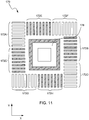
- Fig. 11 is a top plan view of an overlay mark 170, in accordance with an alternate example.
- the overlay mark 170 may generally correspond to the overlay mark shown in Figs. 6 & 9 .
- overlay mark 170 contains eight working zones 172A-H for determining the registration error between two wafer layers in two different directions (one layer is represented by cross-hatching, the other is not).
- Each of the working zones includes a periodic structure 174 comprised by a plurality of coarsely segmented lines 176.
- each of the working zones 172 are configured to accommodate an additional structure 178 in the center of the mark 170.
- the working zones 172A-H are disposed around the outer region of the mark while the additional structure 178 is disposed in the center of the mark.
- the additional structure 178 may represent a standard box in box structure as described in the background of this application.
- the mark 170 can be acquired and measured by standard box in box metrology tools and algorithms, i.e., existing equipment and software may be used.
- Fig. 12 is a top plan view of an overlay mark 190, in accordance with an alternate example.
- overlay mark 190 may correspond to the mark of Fig. 9 .
- the overlay mark 190 of Fig. 12 is configured to measure overlay in two separate directions. As such, mark 190 obviates the need to have one mark for each direction in which overlay needs to be measured.
- the mark 190 includes triangularly shaped working zones. Overlay mark 190 is shown in a configuration that results when the tested layers of a wafer are in perfect alignment.
- the overlay mark 190 includes a plurality of working zones 192 for determining the registration error between two wafer layers in two different directions.
- the overlay mark 140 includes eight triangularly shaped working zones 192, which are configured to substantially fill its perimeter.
- the working zones 192 represent the actual areas of the mark that are used to calculate alignment between different layers of the wafer.
- the working zones 192 are spatially separated from one another so that they do not overlap portions of an adjacent working zone. In this particular configuration, all of the working zones 192 are separated via exclusion zones 193.
- the working zones 192 are grouped into a first working group 194 and a second working group 196.
- the first working group 194 includes four working zones 192A-D that are configured to provide overlay information in a first direction.
- the first direction may be the Y direction.
- two of them 192A and D are disposed in the first layer and two of them 192 B and C are disposed in the second layer (the first layer is represented by solid lines, the second layer is represented by dashed lines).
- the centers of symmetry 195 of working zones 192A&D and working zones 192B&C coincide exactly.
- the second working group 196 includes four working zones 192E-H configured to provide overlay information in a second direction that is perpendicular to the first direction.
- the second direction may be the X direction.
- the four working zones 192E-H two of them 192 E and H are disposed in the first layer and two of them 192 F and G are disposed in the second layer (the first layer is represented by solid lines, the second layer is represented by dashed lines).
- the centers of symmetry 197 of working zones 192E&H and working zones 192F&G coincide exactly.
- all of the working zones 192 are equally positioned relative to the center of the mark.
- each of the groups 194 and 196 represents an "X" - configured mark.
- working group 194 includes working zones 192A&D, which are on the same first layer and in diagonally opposed positions relative to one another, and working zones 192B&C, which are on the same second layer and in diagonally opposed positions relative to one another.
- working zones 192A&D are angled relative to working zones 192B&C.
- working zone 192A is spatially offset from working zone 192D
- working zone 192B is spatially offset from working zone 192D.
- working group 136 includes working zones 192E&H, which are on the same first layer and in opposed positions relative to one another, and working zones 192F&G, which are on the same second layer and in opposed positions relative to one another. Further, working zones 192E&H are angled relative to working zones 192F&G. Further still, working zone 192E is spatially offset from working zone 192H, and working zone 192F is spatially offset from working zone 192G. In essence, this particular mark produces two "X" configured marks that are positioned orthogonal to each other, i.e., working group 194 and working group 196.
- a working zone on one layer is generally juxtaposed relative to a working zone on another layer.
- working zone 192A is juxtaposed relative to working zone 192B and working zone 192C is juxtaposed relative to working zone 192D.
- working zone 192E is juxtaposed relative to working zone 192H and working zone 192F is juxtaposed relative to working zone 192G.
- all of the working zones 192 are equally positioned relative to the center of the mark.
- juxtaposed pairs are positioned in an opposed relationship (e.g., upper/lower and right/left) relative to the other juxtaposed pair in the group.
- juxtaposed pairs 192A&B are positioned opposite juxtaposed pairs 192C&D
- juxtaposed pairs 192E&F are positioned opposite juxtaposed pairs 192G&H.
- the configuration of the working zones is rotationally symmetric ( ⁇ 90, 180, 270, 360 degrees around the center of the mark) without biasing the center or periphery with one or other layer, i.e., the mark is invariant.
- This is typically done to reduce the impact of radial and axial variations across the field of view of the metrology tool, as for example, radial and axial variations caused by optical aberrations and illuminations that may cause tool induced shifts (TIS).
- TIS tool induced shifts
- Each of the working zones 192 includes a periodic structure 198 comprised by a plurality of coarsely segmented lines 200.
- the linewidths, D, and spacings, s, of the coarsely segmented lines may be widely varied.
- each of the periodic structures 198 substantially fills the perimeter of its corresponding working zone 192.
- the periodic structures 198 are also disposed on the layer of its corresponding work zone 192.
- the periodic structures 198 may be broken up into a first periodic structure 198A that is associated with the first working group 194 and a second periodic structure 198B that is associated with the second working group 196.
- the first periodic structures 198A are all oriented in the same direction, i.e., the coarsely segmented lines 190A are parallel and horizontally positioned relative to each other.
- the second periodic structures 198B are also all oriented in the same direction (albeit differently than the first periodic structures), i.e., the coarsely segmented lines 198B are parallel and vertically positioned relative to each other.
- the periodic structures 198A in the first working group 194 are orthogonal to the periodic structures 198B in the second working group 196.
- the coarsely segmented lines 190 decrease in length as they move from the outer regions of the mark to the inner regions of the mark.
- the coarsely segmented line may be formed by a plurality of finely segmented elements to further enhance this mark.
- Fig. 13 is a top plan view of an overlay mark 210, in accordance with an alternate example.
- mark 210 has the same general layout and characteristics as mark 190 of Fig. 12 , i.e., eight triangularly shaped working zones.
- Mark 210 differs from mark 190, however, in that it biases the center of the mark with a grating pattern 212 formed on one of the two layers.
- the grating pattern 212 is typically used in cases where the mark quality in one layer is poorer than the mark quality in the other layer due to contrast or graininess. That is, the information (e.g., edges) in a layer where contrast is low is increased.
- biasing the center of the FOV with one layer may protect it from process damage.
- the grating pattern 212 may be widely varied.
- grating pattern may include any number of lines in any number of distributions and sizes.
- the grating pattern is formed on the second layer and it consists of groups of two coarsely segmented lines 214 that alternate in direction (e.g., X and Y directions) around the center of the mark.
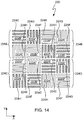
- Fig. 14 is a top plan view of an overlay mark 220, in accordance with an alternate example.
- overlay mark 220 may generally correspond to the overlay mark shown in Fig. 9 .
- overlay mark 220 is configured to measure overlay in two separate directions. As such, mark 220 obviates the need to have one mark for each direction in which overlay needs to be measured.
- Overlay mark 220 is shown in a configuration that results when the tested layers of a wafer are in perfect alignment.
- the overlay mark 220 includes a plurality of working zones 222 for determining the registration error between two wafer layers in two different directions.
- the overlay mark 222 includes sixteen square shaped working zones 222, which are configured to substantially fill its perimeter.
- Each of the working zones 222 includes a periodic structure of coarsely segmented lines.
- the coarsely segmented lines may be formed by a plurality of finely segmented elements, as for example, any configuration described or shown herein (i.e., Figs. 3-5 ).
- the working zones 222A are oriented in the X direction and 8 of the working zones 222B are oriented in the Y direction (as shown by the periodic structures disposed therein).
- 4 of the working zones 222' are printed in a first layer (represented by cross hatching) while 4 of the working zones 222" are printed in a second layer (not represented by cross hatching).
- the orientation of the working zones may be described in a variety of ways.
- the working zones 222 may be distributed into four groups 224A-D that form the four corners of the square shaped mark 220.
- Each of these groups 224A-D is equally represented by working zones formed on different layers and in different direction. That is, each group includes four different working zones, as for example, working zones 222A', 222A", 222B' and 222B".
- the working zones 222 may also be distributed into four groups 224E-H, each of which represents an "X" - configured mark (albeit offset).
- the "X"-configured mark is formed by the corners of a 3 by 3 working zone group.
- two of them determine overlay in the X-direction and two of them determine overlay in the Y direction.
- working group 224E and F which include diagonally opposed and spatially offset working zones 222B'& 222B"
- working group 224G and H which include diagonally opposed and spatially offset working zones 222A'& 222A" determine overlay in the X-direction.
- Fig. 15 is a top plan view of an overlay mark 240, in accordance with an alternate example.
- overlay mark 240 may generally correspond to the overlay mark shown in Fig. 14 .
- overlay mark 240 is configured to measure overlay in two separate directions. As such, mark 240 obviates the need to have one mark for each direction in which overlay needs to be measured.
- Overlay mark 240 is shown in a configuration that results when the tested layers of a wafer are in perfect alignment.
- the overlay mark 240 includes a plurality of working zones 242 for determining the registration error between two wafer layers in two different directions.
- the overlay mark 240 includes sixteen square shaped working zones 242, which are configured to substantially fill its perimeter.
- Each of the working zones 242 includes a periodic structure of coarsely segmented lines. Although not shown, it should be appreciated that in some cases the coarsely segmented lines may be formed by a plurality of finely segmented elements.
- 8 of the working zones 242A are oriented in the X direction and 8 of the working zones 242B are oriented in the Y direction (as shown by the periodic structures disposed therein).
- 8 of the working zones 242 in any given orientation (A or B), 4 of the working zones 242' are printed in a first layer (represented by cross hatching) while 4 of the working zones 242" are printed in a second layer (not represented by cross hatching).
- the orientation of the working zones may be described in a variety of ways.
- the working zones 242 may be distributed into four groups 244A-D that form the four corners of the square shaped mark 240.
- the groups that are opposed at vertical angles are identical, i.e., the working zones therein are oriented the same way.
- each group 244A-D Of the four working zones in each group 244A-D, two of them represent the same layer and direction, and two of them represent a different same layer and direction.
- the working zones that are opposed at vertical angles to one another in these groups are identical, i.e., they represent the same layer and direction.
- groups 244A & D include opposed working zones 242A' and opposed working zones 242B
- groups 244B & C include opposed working zones 242B' and opposed working zones 242A".
- the working zones 242 may also be distributed into four groups 244E-H, each of which represents an "X" - configured mark (albeit offset).
- the "X"-configured mark is formed by the corners of a 3 by 3 working zone group.
- two of them determine overlay in the X-direction and two of them determine overlay in the Y direction.
- working group 244E and F which include opposing working zones 242B'& 242B
- working group 244G and H which include opposing working zones 242A'& 242A" determine overlay in the X-direction.
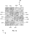
- Fig. 16 is a top plan view of an overlay mark 250, in accordance with an alternate example.
- overlay mark 250 may generally correspond to the overlay mark shown in Fig. 13 .
- overlay mark 250 is configured to measure overlay in two separate directions. As such, mark 250 obviates the need to have one mark for each direction in which overlay needs to be measured.
- Overlay mark 250 is shown in a configuration that results when the tested layers of a wafer are in perfect alignment.
- the overlay mark 250 includes a plurality of working zones 252 for determining the registration error between two wafer layers in two different directions.
- the overlay mark 250 includes sixteen square shaped working zones 252, which are configured to substantially fill its perimeter.
- Each of the working zones 252 includes a periodic structure of coarsely segmented lines. Although not shown, it should be appreciated that in some cases the coarsely segmented lines may be formed by finely segmented elements.
- the working zones 252A are oriented in the X direction and 8 of the working zones 252B are oriented in the Y direction (as shown by the periodic structures disposed therein).
- 8 of the working zones 252' are printed in a first layer (represented by cross hatching) while 4 of the working zones 252" are printed in a second layer (not represented by cross hatching).
- the working zones 252 may be distributed into four groups 254E-H, each of which represents an "X" - configured mark (albeit offset). In this case, the "X"-configured mark is formed by the corners of a 3 by 3 working zone group.
- working group 254E and F which include opposing working zones 252B'& 252B"
- working group 254G and H which include opposing working zones 252A'& 252A”
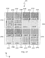
- Fig. 17 is a top plan view of an overlay mark 270, in accordance with an alternate example.
- overlay mark 270 may generally correspond to the overlay mark shown in Fig. 13 .
- overlay mark 270 is configured to measure overlay in two separate directions. As such, mark 270 obviates the need to have one mark for each direction in which overlay needs to be measured.
- Overlay mark 270 is shown in a configuration that results when the tested layers of a wafer are in perfect alignment.
- the overlay mark 270 includes a plurality of working zones 272 for determining the registration error between two wafer layers in two different directions.
- the overlay mark 270 includes sixteen square shaped working zones 272, which are configured to substantially fill its perimeter.
- Each of the working zones 272 includes a periodic structure of coarsely segmented lines. Although not shown, it should be appreciated that in some cases the coarsely segmented lines may be formed by finely segmented elements.
- 8 of the working zones 272A are oriented in the X direction and 8 of the working zones 272B are oriented in the Y direction (as shown by the periodic structures disposed therein).
- 8 of the working zones 272' are printed in a first layer (represented by cross hatching) while 4 of the working zones 272" are printed in a second layer (not represented by cross hatching).
- 4 of the working zones 272 in any given orientation (A or B), 4 of the working zones 272 have a periodic structure M with a first period (represented by thinner lines) while 4 of the working zones 272 have a periodic structure N with a second period that is different than the first period (represented by wider lines).
- the orientation of the working zones may be described in a variety of ways.
- the working zones 272 may be distributed into four groups 274A-D that form the four corners of the square shaped mark 270.
- the groups that are opposed at vertical angles are identical, i.e., the working zones therein are oriented the same way.
- Each of these groups 274A-D includes four different working zones, which may represent different combinations of layers, directions or period.
- the working zones that are opposed at vertical angles to one another in these groups represent the same direction, but different layers and periods.
- groups 272A & D include working zone 272A-M' that is opposed to working zone 272B-N' and working zone 272A-M" that is opposed to working zone 272B-N", and groups 272B & C include working zone 272B-M' that is opposed to working zone 272A-N' and working zone 272B-M" is opposed to working zone 272A-N".
- the working zones 272 may also be distributed into four groups 274E-H, each of which represents an "X" - configured mark (albeit offset).
- the "X"-configured mark is formed by the corners of a 3 by 3 working zone group.
- two of them determine overlay in the X-direction and two of them determine overlay in the Y direction.
- two of them represent a first period and two of them represent a second period.
- working group 274E which includes opposing working zones 272B-M'& 272B-M
- working group 274F which includes opposing working zones 272B-N'& 272B-N
- working group 274G which include opposing working zones 272A-M'& 272A-M
- working group 274H which include opposing working zones 272A-N'& 272A-N
- this configuration can result in improved process robustness and/or improved contrast for one of the two grating periods, allowing selection of the optimized period and or line width for a specific process.
- Fig. 18 is a top plan view of an overlay mark 290, in accordance with an alternate example.
- overlay mark 290 may generally correspond to the overlay mark shown in Fig. 13 .
- overlay mark 290 is configured to measure overlay in two separate directions. As such, mark 290 obviates the need to have one mark for each direction in which overlay needs to be measured.
- overlay mark 290 is also configured to determine the relative shift between three successive layers of a wafer or between three separately generated patterns on a single layer of a wafer.
- the overlay mark 290 will be described in context of measuring overlay between different layers of a substrate. It should be noted, however, that the overlay mark in this figure may also be used to measure two or more separately generated patterns on a single layer of a substrate.
- Overlay mark 290 is shown in a configuration that results when the tested layers of a wafer are in perfect alignment.
- the overlay mark 290 includes a plurality of working zones 292 for determining the registration error between three wafer layers in two different directions.
- the overlay mark 290 includes sixteen square shaped working zones 292, which are configured to substantially fill its perimeter7.
- Each of the working zones 292 includes a periodic structure of coarsely segmented lines. Although not shown, it should be appreciated that in some cases the coarsely segmented lines may be formed by finely segmented elements.
- the 16 working zones 292 8 of the working zones 292A are oriented in the X direction and 8 of the working zones 292B are oriented in the Y direction (as shown by the periodic structures disposed therein). Furthermore, 8 of the working zones 292' are printed in a first layer (represented by cross hatching), 4 of the working zones 292" are printed in a second layer (not represented by cross hatching), and 4 of the working zones 292"' are printed in a third layer (represented by fill).
- the first layer also represented by a single prime
- the second layer is disposed over the third layer (also represented by a triple prime).
- the first layer may represent a resist layer
- the second layer may represent a first metal layer
- the third layer may represent a second metal layer.
- each additional pair of gratings may be printed in up to any of 3 previous layers.
- All of the overlay marks described above are configured to at least balance non-uniformities caused by the metrology tool (e.g., aberrations and illumination) and/or by the process (e.g., dishing and erosion). For example, some of the marks may be configured to reduce the impact of radial variations while others may be configured to reduce the impact of axial variations on the overlay measurements.
- the metrology tool e.g., aberrations and illumination
- the process e.g., dishing and erosion
- Fig. 19 is a simplified diagram of an overlay measurement system or metrology tool 320 that may be used to measure overlay in any of the marks described above via imaging.
- Imaging is a very developed technology with large user acceptance, and components that are readily available to the user. As is generally well known, imaging is an effective way to collect a large amount of information at any one time. That is, all points within the mark may be measured simultaneously. Furthermore, imaging allows a user to see what is actually being measured on the wafer. The dimensions of various components are exaggerated to better illustrate this system.
- the overlay measurement system 320 is arranged to determine overlay error via one or more overlay targets 322 disposed on a wafer 324. In most cases, the overlay targets 322 are positioned within the scribe lines of the wafer 324.
- the overlay measurement system 320 includes an optical assembly 326 and a computer 328.
- the optical assembly 326 is generally arranged to capture the images of the overlay target 322.
- the computer is generally arranged to calculate the relative displacement of the elements of the overlay target from the captured images.
- the optical assembly 326 includes a light source 330 (e.g., incoherent or coherent, although incoherent is generally preferred) arranged to emit light 332 along a first path 334.
- the light 332 is made incident on a first lens 335, which focuses the light 332 onto a fiber optic line 336 configured to pass the light 332 therethrough.
- a second lens 338 which is arranged to collimate the light 332.
- the collimated light 332 then continues on its path until it reaches a beam splitter cube 340, which is arranged to direct the collimated light onto a path 342.
- the collimated light 332 continuing along path 342 is made incident on an objective lens 344, which focuses the light 332 onto the wafer 324.
- the reflected light 332 that is collected by the objective lens 344 generally contains an image of a portion of the wafer 324, as for example, the image of the overlay target 322.
- the objective lens 344 manipulates the collected light in a manner that is optically reverse in relation to how the incident light was manipulated. That is, the objective lens 344 re-collimates the light 332 and directs the light 332 towards the beam splitter cube 340.
- the beam splitter cube 340 is arranged to direct the light 332 onto a path 346.
- the light 332 continuing on path 346 is then collected by a tube lens 350, which focuses the light 332 onto a camera 352 that records the image of the wafer 324, and more particularly the image of the target 322.
- the camera 352 may be a charge couple device (CCD), a two-dimensional CCD, or linear CCD array.
- CCD charge couple device
- the camera 352 transforms the recorded image into electrical signals, which can be used by, and which are sent to the computer 328.
- the computer 328 After receiving the electrical signals, the computer 328 performs analysis algorithms that calculate the overlay error of the image. Analysis algorithms will be described in greater detail below.
- the system 320 further includes a frame grabber 354 that works with the computer 328 and the camera 352 to grab images from the wafer 324.
- the frame grabber 354 is shown as a separate component, it should be noted that the frame grabber 354 may be part of the computer 328and/or part of the camera 352.
- the frame grabber 354 typically has two functions-target acquisition and image grab. During target acquisition, the frame grabber 354 and computer 328 cooperate with a wafer stage 356 to place the target in focus and to position the target as closes as possible to the center of the field of view (FOV) of the metrology tool. In most cases, the frame grabber grabs a plurality of images (e.
- FOV field of view
- the stage moves the wafer between these grabs until the target is correctly positioned in the X, Y and Z directions.
- the X & Y directions generally correspond to the field of view (FOV) while the Z direction generally corresponds to the focus.
- the frame grabber determines the correct position of the target, the second of these two functions is implemented (e. g., image grab).
- image grab the frame grabber 354 makes a final grab or grabs so as to capture and store the correctly positioned target images, i. e., the images that are used to determine overlay.
- information must be extracted from the grabbed images to determine the registration error.
- the extracted information may be digital information or in waveforms.
- phase retrieval based analysis typically involves creating one dimensional signals by collapsing each of the working zones by summing pixels along the lines of the periodic structure. Examples of phase retrieval algorithms that may be used are described in U. S. Patent No.
- phase retrieval algorithm decomposes signals into a set of harmonics of the basic signal frequency. Quantitative comparison of different harmonics'amplitudes and phases provide important information concerning signals' symmetry and spectral content. In particular, the phase difference between the 1 st and 2nd or higher harmonics of the same signal (calibrated with their amplitudes) measures the degree of the signal asymmetry.
- Wavelet analysis is somewhat similar to that described in the section above, however, now a dynamic window is moved across the one dimensional signal and the phase estimation is carried out in a more localized way. This is particularly of interest with use in the case of a chirped periodic structure.
- Another group may relate to intensity correlation based methods. In this approach the centers of symmetry for each process layer is found separately by calculating the cross covariance of one signal with the reversed signal from the opposite part of the mark, from the same process layer.
- This technique is similar to techniques used today with regards to box in box targets. The above techniques are brought by way of example and have been tested and demonstrated good performance.
- overlay measurement tool may be any of a number of suitable and known imaging or metrology tools arranged for resolving the critical aspects of overlay marks formed on the surface of the wafer.
- overlay measurement tool may be adapted for bright field imaging microscopy, darkfield imaging microscopy, full sky imaging microscopy, phase contrast microscopy, polarization contrast microscopy, and coherence probe microscopy. It is also contemplated that single and multiple image methods may be used in order to capture images of the target.
- CPM single grab coherence probe microscopy
- double grab CPM methods are readily available commercially.
- single and multiple image methods may be readily available from KLA-Tencor of San Jose, California.
- Fig. 20A is a simplified flow diagram illustrating a method 360 of calculating overlay. For ease of discussion, this method will be described via the mark shown in Fig. 9 . This mark is now shown next to the flow diagram in Fig. 20B .
- the method 360 begins at step 362 where the working zones are selected from the captured image.
- working zones 132 E-H may be selected, and for calculating Y-overlay, working zones 132 A-D may be selected.
- the process flow proceeds to step 364 where representative signals are formed for each of the selected working zones.
- Fig. 20C illustrates a first collapsed 1D signal for working zone 132A and a second collapsed 1D signal for working zone 132B. It should be noted, that Fig. 20C is representative of any of the pairs of juxtaposed working zones.
- this is accomplished via a covariance-based overlay algorithm, which is based upon calculation of the cross-correlation between the patterns belonging to the same process layers. As a result, the centers of symmetry for both layers are found, and their misregistration is essentially the overlay.
- the flowchart of this algorithm is shown in Figure 21 .
- this is accomplished via a Fourier Decomposition overlay algorithm, which utilizes the periodical character of the grating structures.
- This algorithm decomposes signals acquired from the target patterns to a series of Fourier harmonics. Comparison of phases between the same order harmonics from different process layers calibrated to nominal pitch of the grating patterns serves then as a basis for overlay calculation. Accordingly, this algorithm provides several independent overlay results - one for each Fourier order.
- the flowchart of this algorithm is shown in Figure 22 .
- Fig. 21 is a flow diagram illustrating a method 370 of calculating overlay using Covariance, in accordance with one example.
- method 370 may generally correspond to step 366 of Fig. 20A .
- the method 370 begins at step 372 where the signal cross-correlation is calculated. This is typically done with respect to opposing working zones. With regards to the mark of Fig. 9 ., the signal cross-correlation is calculated for working zone pairs 132A vs. reversed 132D, 132B vs. reversed 132C, 132E vs. reversed 132H, and 132F vs. reversed 132G.
- step 374 the positions of cross-correlation maxima (sub pixel) are found. This is typically done for both of the layers, i.e., layer 1, which is represented by cross hatching, and layer 2, which is represented with no cross hatching.
- step 376 the overlay is determined by calculating the difference between the positions of cross correlation maxima. For example, the difference between the cross correlation maxima of working zones 132E&H (layer 1) - working zones 132 F&G (layer 2) determines the misregistration in the X-direction. In addition, the difference between the cross correlation maxima of working zones 132A&D (layer 1) - working zones 132 B&C (layer 2) determines the misregistration in the Y-direction.
- Fig. 22 is a flow diagram illustrating a method 380 of calculating overlay using Fourier Decomposition, in accordance with one example.
- method 380 may generally correspond to step 366 of Fig. 20A .
- the method 380 begins at step 382 where the signals are fitted to a Fourier series and their phases are extracted. After fitting and extracting, the process flow proceeds to step 384 where the phase difference between juxtaposed working zones is found. For example, in the Y direction, the phase difference is found between working zones 132A and 132B, as well as, between working zones 132C and 132D. In addition, in the X direction, the phase difference is found between working zones 132E and 132F, as well as, between working zones 132G and 132H.
- step 386 the overlay is determined by calculating the difference between the phase differences of the previous step for a given direction. For example, the average of the difference between the phase difference of working zones 132E&F and the phase difference of working zones 132 G&H determines the misregistration in the X-direction. In addition, the average of the difference between the phase difference of working zones 132A&B and the phase difference of working zones 132 C&D determines the misregistration in the Y-direction. In order to obtain data that corresponds to positions of the layers, the phase difference is multiplied by the pitch and divided by 2 ⁇ .
- Fig. 23 is a flow diagram illustrating a method 390 of designing an overlay mark.
- the overlay mark may generally correspond to any of the overlay marks described above.
- the overlay mark is generally provided to determine the relative shift between two or more successive layers of a substrate or between two or more separately generated patterns on a single layer of a substrate.
- the overlay mark comprises a plurality of elements that form the pattern of the overlay mark. Each of these elements may be configured to contain information for measuring overlay in a more precise or accurate manner.
- the elements may generally correspond to the working zones, periodic structures of coarsely segmented elements and finely segmented elements.
- the method 390 begins at step 392 where the geometry of a first element of the mark is optimized according to a first scale. This is typically accomplished by identifying the upper and lower limits of the first scale and fine tuning the geometry of the first geometry between the upper and lower limits.
- the first scale corresponds to the metrology kernel scale, which defines the boundaries of the regions that contain information about the two different layers or patterns between which overlay is to be measured.
- the metrology kernel scale has characteristic dimensions in the 10's of microns.
- the metrology kernel scale may range from about 4 micrometer to about 10 microns, and more particularly from about 5 micrometer to about 10 micrometer.
- Metrology tool limitations generally refers to limitations associated with the metrology tool (both for a line of tools and a specific tool within the line).
- metrology tool limitations may include the size and shape of the field of view of the metrology tool used to measure overlay, the minimum amount of target area needed to effectively measure overlay and asymmetrical aberration and illumination field distributions created by the components of the metrology tool.
- Process robustness issues generally refer to restrictions associated with the robustness of the process, as for example, etching, deposition, chemical-mechanical polishing (CMP) and the like. For example, there may be parts of the mark that are more susceptible to process damage or process variation and thus they should be avoided.
- Circuit design criteria generally refers to the rules used to design the overall circuit pattern.
- the circuit design rules may include scribe line limitations that pertain to the overlay mark budget, i.e., the mark is typically positioned inside the scribe line of the wafer.
- the scribe line is the place on the wafer where the wafer separated into a plurality of dies via sawing or dicing.
- the geometry of the first element which generally contains information relating to the layers or patterns between which overlay is measured, may be fine-tuned to find a mark layout that works best within this scale.
- the first element corresponds to working zones, which define the different layers or patterns of the overlay mark, and which represent the actual area of the overlay mark that is used for overlay measurements.
- the term "geometry" generally refers to the size, shape, and/or distribution of the first element, i.e., the working zones.
- fine-tuning is implemented by defining the perimeter of the mark (e.g., FOV) and dividing the mark into a plurality of working zones that are configured to minimize the impact of asymmetries on the measurement of overlay.
- the working zones may be configured to minimize the impact of optical aberrations and illuminations on tool induced shifts in the resultant overlay measurement.
- the working zones may be configured to minimize the impact of process variations on wafer induced shifts in the resultant overlay measurement.
- the process flow proceeds to step 394 where the geometry of a second element of the mark is optimized according to a second scale.
- a second scale corresponds to the image resolution scale, which defines the boundaries between structures within a given process layer.
- the image resolution scale has characteristic dimensions in the 1 micrometer range.
- the image resolution scale may range from about 0.3 micrometer to about 2 micrometer, and more particularly from about .5 micrometer to about 1 micrometer.
- Metrology tool limitations generally refers to limitations associated with the metrology tool (both for a line of tools and a specific tool within the line).
- metrology tool limitations may include the image resolution of the tool, i.e., the ability to capture an image, the algorithms used by the tool to calculate the overlay error and the aberration and illumination field distributions of the tool.
- Process robustness issues generally refer to restrictions that are created by the materials and processes that are used to form the layers and patterns on the wafer, as for example, etching, deposition, chemical-mechanical polishing (CMP) and the like.
- the geometry of the second element is advantageous for the geometry of the second element to be one micron or less in order to diminish the impact of asymmetries resultant from the polishing and aluminum deposition processes.
- the lines be larger than 1 micrometer, as for example, up to two micrometer.
- the geometry of the second element which generally contains the actual spatial information regarding the relative positions of the mark components that is encoded and transferred to the metrology tool, may be fine-tuned to find a mark layout that works best within this scale.
- the second element corresponds to a periodic structure of coarsely segmented lines that is positioned within each of the working zones of the first element.
- the term "geometry" generally refers to the size, shape, and/or distribution of the second element i.e., the periodic structure of coarsely segmented lines (e.g., linewidths and spacings).
- the periodic structures via the coarsely segmented lines are configured to enhance the measurement of overlay by balancing the image resolution of the tool with the process.
- the process flow proceeds to step 396 where the geometry of a third element of the mark is optimized according to a third scale.
- a third scale corresponds to the lithography resolution scale, which defines the boundaries of sub-structures within a given structure.
- the lithography resolution scale has characteristic dimensions in the 0.1 micrometer range.
- the lithography resolution scale may range from about 0.01 micrometer to about 0.5 micrometer, and more particularly from about .05 micrometer to about .18 micrometer.
- Circuit design rules generally refer to the rules used to design the overall circuit pattern.
- the circuit design rules may include the geometry of the circuit devices (e.g., feature size and density).
- Process robustness issues generally refer to restrictions that are created by the materials and processes that are used to form the layers and patterns on the wafer, as for example, etching, deposition, chemical-mechanical polishing (CMP) and the like.
- Metrology tool limitations generally refer to limitations associated with the metrology tool (both for a line of tools and a specific tool within the line).
- metrology tool limitations may include contrast requirements of the tool, i.e., the ability to resolve the larger structures, which are comprised by the smaller sub-structures.
- the geometry of the third element which generally contains information reflective of the circuit structures themselves, may be fine-tuned to find a mark layout that works best within this scale.
- the third element corresponds to the finely segmented elements that form the plurality of coarsely segmented lines of the periodic structures of the second element.
- the term "geometry" generally refers to the size, shape, and/or distribution of the third element, i.e., the finely segmented elements.
- the finely segmented elements are configured to minimize the adverse effects of the process so as to improve the accuracy and precision of the overlay measurements.
- the structure is optimized so as to minimize the difference in stepper PPE between the target and the actual device, as described previously in Figs 3-5 .
Claims (17)
- Substrat ayant un repère de superposition (70) pour déterminer le décalage relatif entre au moins deux couches successives du substrat ou entre au moins deux motifs générés séparément sur une unique couche du substrat, ladite ou lesdites couches comprenant des caractéristiques de motif de circuit intégré, le repère de superposition comprenant :au moins un motif de test pour déterminer le décalage relatif entre une première et une deuxième couche du substrat, ou entre un premier et un deuxième motif généré séparément sur une unique couche du substrat, dans une première direction, le motif de test ayant un premier ensemble de zones de travail (72A, 72D) et un deuxième ensemble de zones de travail (72B, 72C), le premier ensemble de zones de travail (72A, 72D) étant disposé sur la première couche du substrat, ou formé par le premier motif sur l'unique couche, et ayant au moins deux zones de travail (72A, 72D) diagonalement opposées et spatialement décalées l'une par rapport à l'autre, le deuxième ensemble de zones de travail (72B, 72C) étant disposé sur la deuxième couche du substrat, ou formé par le deuxième motif sur l'unique couche, et ayant au moins deux zones de travail (72B, 72C) diagonalement opposées et spatialement décalées l'une par rapport à l'autre ;dans lequel le substrat comprend en outre une structure périodique (74) positionnée à l'intérieur de chacune des zones de travail (72), chacune des structures périodiques (74) comprenant une pluralité d'éléments grossièrement segmentés (76) ; caractérisé en ce que :la pluralité d'éléments grossièrement segmentés (76) est formée par une pluralité d'éléments finement segmentés (78) qui ont des dimensions comparables aux dimensions critiques du circuit intégré ; etles éléments grossièrement et finement segmentés (76, 78) comprennent des lignes grossièrement segmentées (76) qui sont formées par une pluralité de barres finement segmentées (78) et au moins un champ sombre (81), la pluralité de lignes grossièrement segmentées étant séparée par une pluralité de barres finement segmentées (78) et au moins un champ clair (82).
- Substrat selon la revendication 1, dans lequel les éléments grossièrement segmentés (76) sont orientés dans une première direction.
- Substrat selon la revendication 1, dans lequel les zones de travail (72) sont séparées par des zones d'exclusion (80).
- Substrat selon la revendication 1, dans lequel, pour chaque zone de travail (72) dans la première couche, il existe une zone de travail (72) correspondante dans la deuxième couche.
- Substrat selon la revendication 1, dans lequel le premier ensemble de zones de travail (72A, 72D) est incliné par rapport au deuxième ensemble de zones de travail (72B, 72C).
- Substrat selon la revendication 1, dans lequel les zones de travail (72) sont séparées spatialement l'une de l'autre de manière qu'elles ne chevauchent pas des portions d'une zone de travail adjacente (72).
- Substrat selon la revendication 1, dans lequel les éléments grossièrement segmentés (76) sont des lignes parallèles.
- Substrat selon la revendication 1, comprenant en outre un deuxième motif de test pour déterminer le décalage relatif entre une première et une deuxième couche du substrat dans une deuxième direction.
- Substrat selon la revendication 8, dans lequel le deuxième motif de test est orthogonal au premier motif de test.
- Substrat selon la revendication 8, dans lequel la première direction correspond à la direction X, et la deuxième direction correspond à la direction Y.
- Substrat selon la revendication 8, comprenant en outre un troisième motif de test et un quatrième motif de test pour déterminer le décalage relatif entre une première et une deuxième couche du substrat, respectivement dans les première et deuxième directions.
- Substrat selon la revendication 1, dans lequel la première couche est disposée directement au-dessus ou au-dessous de la deuxième couche.
- Procédé pour déterminer le décalage relatif entre au moins deux couches successives d'un substrat ou entre au moins deux motifs générés séparément sur une unique couche d'un substrat, ladite ou lesdites couches comprenant des caractéristiques de motif de circuit intégré, le procédé comprenant :la capture d'une image d'un repère de superposition (70) formé sur le substrat, le repère de superposition (70) comprenant :au moins un motif de test pour déterminer le décalage relatif entre une première et une deuxième couche ou entre un premier et un deuxième motif généré séparément dans une première direction, le motif de test ayant un premier ensemble de zones de travail (72A, 72D) et un deuxième ensemble de zones de travail (72B, 72C), le premier ensemble (72A, 72D) étant disposé sur la première couche ou formé par le premier motif et ayant au moins deux zones de travail (72A, 72D) diagonalement opposées etspatialement décalées l'une par rapport à l'autre, le deuxième ensemble (72B, 72C) étant disposé sur la deuxième couche ou formé par le deuxième motif et ayant au moins deux zones de travail (72B, 72C) diagonalement opposées et spatialement décalées l'une par rapport à l'autre ;la sélection d'une pluralité de zones de travail (72) à partir de l'image capturée, dans lequel au moins une zone de travail (72) est sélectionnée à partir de chaque couche ou motif ;la formation de signaux représentatifs pour chacune des zones de travail sélectionnées (72), dans lequel au moins un signal pour chaque couche ou motif est formé ; etla comparaison du signal provenant d'une première couche ou d'un premier motif à un signal provenant d'une deuxième couche ou d'un deuxième motif pour déterminer le décalage relatif entre différentes couches ou différents motifs ;dans lequel le repère de superposition comprend en outre une structure périodique (74) positionnée à l'intérieur de chacune des zones de travail (72), chacune des structures périodiques (74) comprenant une pluralité d'éléments grossièrement segmentés (76) ; caractérisé en ce que :la pluralité d'éléments grossièrement segmentés (76) est formée par une pluralité d'éléments finement segmentés (78) qui ont des dimensions comparables aux dimensions critiques du circuit intégré ; etles éléments grossièrement et finement segmentés (76, 78) comprennent des lignes grossièrement segmentées (76) qui sont formées par une pluralité de barres finement segmentées (78) et au moins un champ sombre (81), la pluralité de lignes grossièrement segmentées étant séparée par une pluralité de barres finement segmentées (78) et au moins un champ clair (82).
- Procédé selon la revendication 13, dans lequel la formation de signaux représentatifs est accomplie en écrasant les images 2D des zones de travail (72) en signaux 1D en faisant la moyenne sur X pour des calculs de superposition de Y et faisant la moyenne sur Y pour des calculs de superposition de X.
- Procédé selon la revendication 13, dans lequel la comparaison du signal provenant d'une première couche ou d'un premier motif à un signal provenant d'une deuxième couche ou d'un deuxième motif pour déterminer le décalage relatif entre différentes couches ou différents motifs est accomplie par le biais d'un algorithme de superposition basé sur la covariance.
- Procédé selon la revendication 13, dans lequel la comparaison du signal provenant d'une première couche ou d'un premier motif à un signal provenant d'une deuxième couche ou d'un deuxième motif pour déterminer le décalage relatif entre différentes couches ou différents motifs est accomplie par le biais d'un algorithme de superposition de décomposition de Fourier.
- Procédé selon la revendication 13, dans lequel le déplacement relatif entre les première et deuxième couches de la plaquette ou entre les deux motifs générés séparément sur une unique couche est déterminé en comparant les positions relatives des structures périodiques (74) sur différentes couches ou différents motifs.
Applications Claiming Priority (13)
| Application Number | Priority Date | Filing Date | Title |
|---|---|---|---|
| US22925600P | 2000-08-30 | 2000-08-30 | |
| US229256P | 2000-08-30 | ||
| US30176301P | 2001-06-27 | 2001-06-27 | |
| US30148401P | 2001-06-27 | 2001-06-27 | |
| US30161301P | 2001-06-27 | 2001-06-27 | |
| US30159101P | 2001-06-27 | 2001-06-27 | |
| US301591P | 2001-06-27 | ||
| US09/894,987 US7068833B1 (en) | 2000-08-30 | 2001-06-27 | Overlay marks, methods of overlay mark design and methods of overlay measurements |
| US301613P | 2001-06-27 | ||
| US301484P | 2001-06-27 | ||
| US894987 | 2001-06-27 | ||
| US301763P | 2001-06-27 | ||
| PCT/US2001/041932 WO2002019415A1 (fr) | 2000-08-30 | 2001-08-28 | Repere de recouvrement, procedes servant a concevoir des reperes de recouvrement et procedes de mesure de recouvrement |
Publications (2)
| Publication Number | Publication Date |
|---|---|
| EP1314198A1 EP1314198A1 (fr) | 2003-05-28 |
| EP1314198B1 true EP1314198B1 (fr) | 2017-03-08 |
Family
ID=27559199
Family Applications (1)
| Application Number | Title | Priority Date | Filing Date |
|---|---|---|---|
| EP01971384.1A Expired - Lifetime EP1314198B1 (fr) | 2000-08-30 | 2001-08-28 | Repere de superposition, procedes servant a concevoir des reperes de superposition et procedes de mesure de superposition |
Country Status (3)
| Country | Link |
|---|---|
| EP (1) | EP1314198B1 (fr) |
| JP (8) | JP5180419B2 (fr) |
| WO (1) | WO2002019415A1 (fr) |
Cited By (2)
| Publication number | Priority date | Publication date | Assignee | Title |
|---|---|---|---|---|
| CN110034098A (zh) * | 2018-01-12 | 2019-07-19 | 中芯国际集成电路制造(上海)有限公司 | 半导体结构及其形成方法 |
| EP4174578A1 (fr) * | 2021-11-02 | 2023-05-03 | Commissariat à l'énergie atomique et aux énergies alternatives | Structure de metrologie |
Families Citing this family (78)
| Publication number | Priority date | Publication date | Assignee | Title |
|---|---|---|---|---|
| JP5180419B2 (ja) * | 2000-08-30 | 2013-04-10 | ケーエルエー−テンカー・コーポレーション | 重ね合わせマーク、重ね合わせマークの設計方法および重ね合わせ測定の方法 |
| US7317531B2 (en) * | 2002-12-05 | 2008-01-08 | Kla-Tencor Technologies Corporation | Apparatus and methods for detecting overlay errors using scatterometry |
| US7541201B2 (en) | 2000-08-30 | 2009-06-02 | Kla-Tencor Technologies Corporation | Apparatus and methods for determining overlay of structures having rotational or mirror symmetry |
| CN1495540B (zh) | 2002-09-20 | 2010-08-11 | Asml荷兰有限公司 | 利用至少两个波长的光刻系统的对准系统和方法 |
| JP4746987B2 (ja) * | 2002-12-05 | 2011-08-10 | ケーエルエー−テンカー コーポレイション | 散乱計測を用いてオーバレイ誤差を検出する装置および方法 |
| KR20060009248A (ko) * | 2003-04-08 | 2006-01-31 | 에이오티아이 오퍼레이팅 컴퍼니 인코포레이티드 | 오버레이 측정 마크 |
| EP1614153A2 (fr) * | 2003-04-08 | 2006-01-11 | AOTI Operating Company, Inc. | Marque pour la metrologie par superposition |
| SG108975A1 (en) * | 2003-07-11 | 2005-02-28 | Asml Netherlands Bv | Marker structure for alignment or overlay to correct pattern induced displacement, mask pattern for defining such a marker structure and lithographic projection apparatus using such a mask pattern |
| US6937337B2 (en) | 2003-11-19 | 2005-08-30 | International Business Machines Corporation | Overlay target and measurement method using reference and sub-grids |
| JP4734261B2 (ja) * | 2004-02-18 | 2011-07-27 | ケーエルエー−テンカー コーポレイション | 連続変化するオフセットマークと、オーバレイ決定方法 |
| US7065737B2 (en) * | 2004-03-01 | 2006-06-20 | Advanced Micro Devices, Inc | Multi-layer overlay measurement and correction technique for IC manufacturing |
| US7678516B2 (en) | 2004-07-22 | 2010-03-16 | Kla-Tencor Technologies Corp. | Test structures and methods for monitoring or controlling a semiconductor fabrication process |
| DE102005007280B4 (de) * | 2005-02-17 | 2009-06-10 | Qimonda Ag | Verfahren zum Bestimmen einer kritischen Dimension einer lateral strukturierten Schicht |
| JP4520429B2 (ja) * | 2005-06-01 | 2010-08-04 | エーエスエムエル ネザーランズ ビー.ブイ. | 位置合わせ装置への2次元フォトニック結晶の応用 |
| US7737566B2 (en) | 2005-06-01 | 2010-06-15 | Asml Netherlands B.V. | Alignment devices and methods for providing phase depth control |
| KR100612410B1 (ko) | 2005-08-01 | 2006-08-16 | 나노메트릭스코리아 주식회사 | 오버레이 키, 이를 이용한 오버레이 측정방법 및 측정장치 |
| US7751047B2 (en) * | 2005-08-02 | 2010-07-06 | Asml Netherlands B.V. | Alignment and alignment marks |
| US7439001B2 (en) | 2005-08-18 | 2008-10-21 | International Business Machines Corporation | Focus blur measurement and control method |
| US7687925B2 (en) * | 2005-09-07 | 2010-03-30 | Infineon Technologies Ag | Alignment marks for polarized light lithography and method for use thereof |
| US7474401B2 (en) | 2005-09-13 | 2009-01-06 | International Business Machines Corporation | Multi-layer alignment and overlay target and measurement method |
| DE102005046973B4 (de) * | 2005-09-30 | 2014-01-30 | Globalfoundries Inc. | Struktur und Verfahren zum gleichzeitigen Bestimmen einer Überlagerungsgenauigkeit und eines Musteranordnungsfehlers |
| US7863763B2 (en) | 2005-11-22 | 2011-01-04 | Asml Netherlands B.V. | Binary sinusoidal sub-wavelength gratings as alignment marks |
| US7898662B2 (en) | 2006-06-20 | 2011-03-01 | Asml Netherlands B.V. | Method and apparatus for angular-resolved spectroscopic lithography characterization |
| US7455939B2 (en) | 2006-07-31 | 2008-11-25 | International Business Machines Corporation | Method of improving grating test pattern for lithography monitoring and controlling |
| US7545520B2 (en) * | 2006-11-15 | 2009-06-09 | Asml Netherlands B.V. | System and method for CD determination using an alignment sensor of a lithographic apparatus |
| US7473502B1 (en) | 2007-08-03 | 2009-01-06 | International Business Machines Corporation | Imaging tool calibration artifact and method |
| US7879515B2 (en) | 2008-01-21 | 2011-02-01 | International Business Machines Corporation | Method to control semiconductor device overlay using post etch image metrology |
| NL1036476A1 (nl) * | 2008-02-01 | 2009-08-04 | Asml Netherlands Bv | Alignment mark and a method of aligning a substrate comprising such an alignment mark. |
| KR20090128337A (ko) * | 2008-06-10 | 2009-12-15 | 어플라이드 머티리얼즈 이스라엘 리미티드 | 반복 패턴을 갖는 물체를 평가하는 방법 및 시스템 |
| US9097989B2 (en) | 2009-01-27 | 2015-08-04 | International Business Machines Corporation | Target and method for mask-to-wafer CD, pattern placement and overlay measurement and control |
| EP2470960A1 (fr) * | 2009-08-24 | 2012-07-04 | ASML Netherlands BV | Procédé et appareil de métrologie, appareil lithographique, cellule de traitement lithographique et substrat comprenant des cibles de métrologie |
| US8804137B2 (en) * | 2009-08-31 | 2014-08-12 | Kla-Tencor Corporation | Unique mark and method to determine critical dimension uniformity and registration of reticles combined with wafer overlay capability |
| US8329360B2 (en) * | 2009-12-04 | 2012-12-11 | Taiwan Semiconductor Manufacturing Company, Ltd. | Method and apparatus of providing overlay |
| US9927718B2 (en) | 2010-08-03 | 2018-03-27 | Kla-Tencor Corporation | Multi-layer overlay metrology target and complimentary overlay metrology measurement systems |
| US10890436B2 (en) | 2011-07-19 | 2021-01-12 | Kla Corporation | Overlay targets with orthogonal underlayer dummyfill |
| US11455737B2 (en) * | 2012-12-06 | 2022-09-27 | The Boeing Company | Multiple-scale digital image correlation pattern and measurement |
| JP6361238B2 (ja) * | 2013-04-23 | 2018-07-25 | 大日本印刷株式会社 | インプリント用モールドおよびインプリント方法 |
| JP6326916B2 (ja) * | 2013-04-23 | 2018-05-23 | 大日本印刷株式会社 | インプリント用モールドおよびインプリント方法 |
| WO2014210381A1 (fr) * | 2013-06-27 | 2014-12-31 | Kla-Tencor Corporation | Mesures de polarisation de cibles de métrologie et conceptions de cibles correspondantes |
| CN106030414B (zh) * | 2014-02-21 | 2018-10-09 | Asml荷兰有限公司 | 目标布置的优化和相关的目标 |
| KR102311479B1 (ko) * | 2014-04-01 | 2021-10-13 | 다이니폰 인사츠 가부시키가이샤 | 임프린트용 몰드 및 임프린트 방법 |
| CN107148597B (zh) | 2014-08-29 | 2020-05-01 | Asml荷兰有限公司 | 度量方法、目标和衬底 |
| JP2016180783A (ja) * | 2015-03-23 | 2016-10-13 | ルネサスエレクトロニクス株式会社 | 半導体装置および半導体装置の製造方法、パターンの重ね合わせ検査方法 |
| IL256196B (en) | 2015-06-17 | 2022-07-01 | Asml Netherlands Bv | Prescription selection based on inter-prescription composition |
| US10062543B2 (en) * | 2015-06-23 | 2018-08-28 | Kla-Tencor Corp. | Determining multi-patterning step overlay error |
| KR101564312B1 (ko) * | 2015-07-07 | 2015-10-29 | (주)오로스 테크놀로지 | 오버레이 마크 및 이를 이용한 오버레이 계측방법 및 반도체 디바이스 제조방법 |
| US9530199B1 (en) | 2015-07-13 | 2016-12-27 | Applied Materials Israel Ltd | Technique for measuring overlay between layers of a multilayer structure |
| EP3403142B1 (fr) * | 2016-01-11 | 2022-11-09 | KLA-Tencor Corporation | Marque de superposition métrologique et procédé |
| US10615084B2 (en) | 2016-03-01 | 2020-04-07 | Asml Netherlands B.V. | Method and apparatus to determine a patterning process parameter, associated with a change in a physical configuration, using measured pixel optical characteristic values |
| US10451412B2 (en) | 2016-04-22 | 2019-10-22 | Kla-Tencor Corporation | Apparatus and methods for detecting overlay errors using scatterometry |
| IL262114B2 (en) * | 2016-04-22 | 2023-04-01 | Asml Netherlands Bv | Determining the stack difference and correcting with the help of the stack difference |
| FR3051591B1 (fr) | 2016-05-17 | 2020-06-19 | Horiba Jobin Yvon Sas | Dispositif et procede de micro-localisation pour instrument imageur et appareil de mesure |
| KR101665569B1 (ko) | 2016-05-19 | 2016-10-12 | (주)오로스 테크놀로지 | 오버레이 마크 및 이를 이용한 오버레이 계측방법 및 반도체 디바이스 제조방법 |
| US10635004B2 (en) * | 2016-11-10 | 2020-04-28 | Asml Netherlands B.V. | Correction using stack difference |
| KR102331099B1 (ko) * | 2017-05-24 | 2021-11-24 | 에이에스엠엘 홀딩 엔.브이. | 정렬 시스템에서 2 차원 정렬을 위한 정렬 마크 |
| EP3422102A1 (fr) * | 2017-06-26 | 2019-01-02 | ASML Netherlands B.V. | Procédés et dispositifs de formation de motifs et appareils de mesure de performance de mise au point d'un appareil lithographique, procédé de fabrication de dispositifs |
| US10474040B2 (en) * | 2017-12-07 | 2019-11-12 | Kla-Tencor Corporation | Systems and methods for device-correlated overlay metrology |
| US11085754B2 (en) * | 2017-12-12 | 2021-08-10 | Kla Corporation | Enhancing metrology target information content |
| JP2021511532A (ja) * | 2018-01-12 | 2021-05-06 | ケーエルエー コーポレイション | 傾斜周期構造を有する計測ターゲット及び方法 |
| US10446367B2 (en) * | 2018-03-07 | 2019-10-15 | Kla-Tencor Corporation | Scan strategies to minimize charging effects and radiation damage of charged particle beam metrology system |
| KR102381168B1 (ko) * | 2018-10-30 | 2022-03-30 | 케이엘에이 코포레이션 | 비대칭 수차의 추정 |
| US11809090B2 (en) | 2020-01-30 | 2023-11-07 | Kla Corporation | Composite overlay metrology target |
| CN112015061A (zh) * | 2020-08-27 | 2020-12-01 | 上海华力集成电路制造有限公司 | 一种套刻精度量测标记及其使用方法 |
| JP2022117091A (ja) | 2021-01-29 | 2022-08-10 | キヤノン株式会社 | 計測装置、リソグラフィ装置及び物品の製造方法 |
| KR102617622B1 (ko) | 2021-04-26 | 2023-12-27 | (주)오로스 테크놀로지 | 오버레이 마크 및 이를 이용한 오버레이 계측방법 및 반도체 디바이스 제조방법 |
| KR20220168828A (ko) | 2021-06-17 | 2022-12-26 | (주)오로스 테크놀로지 | 변위 벡터를 이용한 오버레이 측정 방법 |
| KR20230003842A (ko) | 2021-06-30 | 2023-01-06 | (주)오로스 테크놀로지 | 오버레이 마크 및 이를 이용한 오버레이 계측방법 및 반도체 디바이스 제조방법 |
| KR20230003846A (ko) | 2021-06-30 | 2023-01-06 | (주)오로스 테크놀로지 | 오버레이 마크 및 이를 이용한 오버레이 계측방법 및 반도체 디바이스 제조방법 |
| KR20230003843A (ko) | 2021-06-30 | 2023-01-06 | (주)오로스 테크놀로지 | 오버레이 마크 및 이를 이용한 오버레이 계측방법 및 반도체 디바이스 제조방법 |
| KR102440758B1 (ko) * | 2021-08-17 | 2022-09-06 | (주)오로스 테크놀로지 | 오버레이 마크 및 이를 이용한 오버레이 측정방법 및 반도체 소자의 제조방법 |
| KR20230032478A (ko) | 2021-08-31 | 2023-03-07 | (주)오로스 테크놀로지 | 모아레 패턴을 형성하는 오버레이 마크 및 이를 이용한 오버레이 측정 방법 |
| KR102566129B1 (ko) * | 2022-01-20 | 2023-08-16 | (주) 오로스테크놀로지 | 모아레 패턴을 형성하는 오버레이 마크, 이를 이용한 오버레이 측정방법, 및 반도체 소자의 제조방법 |
| KR20230157703A (ko) | 2022-05-10 | 2023-11-17 | (주) 오로스테크놀로지 | 서로 겹치는 구조물들을 구비한 오버레이 마크 이미지의 프로젝션 방법 및 서로 겹치는 구조물들을 구비한 오버레이 마크 |
| KR20240008074A (ko) | 2022-07-11 | 2024-01-18 | (주) 오로스테크놀로지 | 모아레 패턴을 형성하는 오버레이 마크, 이를 이용한 오버레이 측정 방법, 및 반도체 소자의 제조방법 |
| KR102460132B1 (ko) | 2022-07-19 | 2022-10-31 | (주)오로스 테크놀로지 | 오버레이 마크 및 이를 이용한 오버레이 측정방법 및 반도체 소자의 제조방법 |
| CN115145127B (zh) * | 2022-09-05 | 2022-11-25 | 上海传芯半导体有限公司 | 套刻精度的检测结构及其制备方法、套刻精度的检测方法 |
| KR102545517B1 (ko) | 2022-10-17 | 2023-06-20 | (주)오로스 테크놀로지 | 모아레 패턴을 형성하는 오버레이 마크, 이를 이용한 오버레이 측정 방법, 오버레이 측정 장치, 및 반도체 소자의 제조 방법 |
| KR102580204B1 (ko) | 2023-03-02 | 2023-09-19 | (주)오로스 테크놀로지 | 1차원 오버레이 오차 측정을 위한 오버레이 마크, 이를 이용한 광학 수차 평가 방법, 이를 이용한 오버레이 마크 품질 평가 방법, 오버레이 측정 장치, 오버레이 측정 방법 및 반도체 소자의 제조방법 |
Citations (3)
| Publication number | Priority date | Publication date | Assignee | Title |
|---|---|---|---|---|
| EP0281030A2 (fr) * | 1987-03-03 | 1988-09-07 | International Business Machines Corporation | Mesure d'alignement de caches à modèles de test par la lumière réfléchie |
| EP0634702A1 (fr) * | 1990-03-27 | 1995-01-18 | Canon Kabushiki Kaisha | Méthode et appareil de mesure |
| US5805290A (en) * | 1996-05-02 | 1998-09-08 | International Business Machines Corporation | Method of optical metrology of unresolved pattern arrays |
Family Cites Families (18)
| Publication number | Priority date | Publication date | Assignee | Title |
|---|---|---|---|---|
| US4388386A (en) * | 1982-06-07 | 1983-06-14 | International Business Machines Corporation | Mask set mismatch |
| JPS61222128A (ja) * | 1985-03-27 | 1986-10-02 | Fujitsu Ltd | 投影露光方法 |
| DE3530439A1 (de) * | 1985-08-26 | 1987-02-26 | Siemens Ag | Vorrichtung zum justieren einer mit mindestens einer justiermarke versehenen maske bezueglich eines mit mindestens einer gitterstruktur versehenen halbleiterwafers |
| NL8900991A (nl) * | 1989-04-20 | 1990-11-16 | Asm Lithography Bv | Apparaat voor het afbeelden van een maskerpatroon op een substraat. |
| DE4000785A1 (de) * | 1990-01-12 | 1991-07-18 | Suess Kg Karl | Justiermarken fuer zwei aufeinander einzujustierende objekte |
| JP3284641B2 (ja) * | 1992-09-03 | 2002-05-20 | ソニー株式会社 | 重ね合わせ精度測定機の測定条件の最適化方法、並びにアラインメントマーク形状あるいは露光装置におけるアラインメントマーク測定方式の最適化方法 |
| JPH0917715A (ja) * | 1995-06-29 | 1997-01-17 | Nec Corp | 半導体装置のパターン合わせノギス |
| US6023338A (en) * | 1996-07-12 | 2000-02-08 | Bareket; Noah | Overlay alignment measurement of wafers |
| JP3552884B2 (ja) * | 1997-09-04 | 2004-08-11 | 沖電気工業株式会社 | 重ね合わせ精度測定用パターン |
| JPH11260714A (ja) * | 1998-03-12 | 1999-09-24 | Nikon Corp | 位置検出マーク及びマーク位置検出方法 |
| JP3287321B2 (ja) * | 1998-12-03 | 2002-06-04 | 日本電気株式会社 | 半導体装置の製造方法 |
| JPH11325877A (ja) * | 1998-03-31 | 1999-11-26 | Siemens Ag | 測定誤差を減少させるための方法及び装置 |
| JP2000133576A (ja) * | 1998-10-28 | 2000-05-12 | Nec Corp | 位置ずれ計測マーク及び位置ずれ計測方法 |
| US6037671A (en) * | 1998-11-03 | 2000-03-14 | Advanced Micro Devices, Inc. | Stepper alignment mark structure for maintaining alignment integrity |
| US6084679A (en) * | 1999-04-02 | 2000-07-04 | Advanced Micro Devices, Inc. | Universal alignment marks for semiconductor defect capture and analysis |
| US6612159B1 (en) * | 1999-08-26 | 2003-09-02 | Schlumberger Technologies, Inc. | Overlay registration error measurement made simultaneously for more than two semiconductor wafer layers |
| JP2001267202A (ja) * | 2000-03-15 | 2001-09-28 | Matsushita Electric Ind Co Ltd | 重ね合わせ測定マーク及びその測定方法と重ね合わせ測定マークを有する半導体装置 |
| JP5180419B2 (ja) * | 2000-08-30 | 2013-04-10 | ケーエルエー−テンカー・コーポレーション | 重ね合わせマーク、重ね合わせマークの設計方法および重ね合わせ測定の方法 |
-
2001
- 2001-08-28 JP JP2002524212A patent/JP5180419B2/ja not_active Expired - Lifetime
- 2001-08-28 EP EP01971384.1A patent/EP1314198B1/fr not_active Expired - Lifetime
- 2001-08-28 WO PCT/US2001/041932 patent/WO2002019415A1/fr active Application Filing
-
2012
- 2012-01-19 JP JP2012009434A patent/JP5663504B2/ja not_active Expired - Lifetime
-
2014
- 2014-05-12 JP JP2014098674A patent/JP5945294B2/ja not_active Expired - Lifetime
-
2015
- 2015-11-09 JP JP2015219296A patent/JP6313272B2/ja not_active Expired - Lifetime
- 2015-11-09 JP JP2015219288A patent/JP2016026331A/ja not_active Withdrawn
-
2016
- 2016-11-24 JP JP2016227754A patent/JP2017040941A/ja active Pending
- 2016-11-24 JP JP2016228018A patent/JP2017062492A/ja active Pending
-
2020
- 2020-03-10 JP JP2020040921A patent/JP2020112807A/ja active Pending
Patent Citations (3)
| Publication number | Priority date | Publication date | Assignee | Title |
|---|---|---|---|---|
| EP0281030A2 (fr) * | 1987-03-03 | 1988-09-07 | International Business Machines Corporation | Mesure d'alignement de caches à modèles de test par la lumière réfléchie |
| EP0634702A1 (fr) * | 1990-03-27 | 1995-01-18 | Canon Kabushiki Kaisha | Méthode et appareil de mesure |
| US5805290A (en) * | 1996-05-02 | 1998-09-08 | International Business Machines Corporation | Method of optical metrology of unresolved pattern arrays |
Cited By (2)
| Publication number | Priority date | Publication date | Assignee | Title |
|---|---|---|---|---|
| CN110034098A (zh) * | 2018-01-12 | 2019-07-19 | 中芯国际集成电路制造(上海)有限公司 | 半导体结构及其形成方法 |
| EP4174578A1 (fr) * | 2021-11-02 | 2023-05-03 | Commissariat à l'énergie atomique et aux énergies alternatives | Structure de metrologie |
Also Published As
| Publication number | Publication date |
|---|---|
| JP2016026331A (ja) | 2016-02-12 |
| JP2020112807A (ja) | 2020-07-27 |
| JP2017062492A (ja) | 2017-03-30 |
| JP2004508711A (ja) | 2004-03-18 |
| JP2014160868A (ja) | 2014-09-04 |
| JP6313272B2 (ja) | 2018-04-18 |
| JP2016026332A (ja) | 2016-02-12 |
| WO2002019415A1 (fr) | 2002-03-07 |
| JP5945294B2 (ja) | 2016-07-05 |
| JP5180419B2 (ja) | 2013-04-10 |
| JP2012080131A (ja) | 2012-04-19 |
| JP5663504B2 (ja) | 2015-02-04 |
| EP1314198A1 (fr) | 2003-05-28 |
| JP2017040941A (ja) | 2017-02-23 |
Similar Documents
| Publication | Publication Date | Title |
|---|---|---|
| EP1314198B1 (fr) | Repere de superposition, procedes servant a concevoir des reperes de superposition et procedes de mesure de superposition | |
| US9702693B2 (en) | Apparatus for measuring overlay errors | |
| US7879627B2 (en) | Overlay marks and methods of manufacturing such marks | |
| JP2016026331A5 (fr) | ||
| JP2016026332A5 (fr) | ||
| US7408642B1 (en) | Registration target design for managing both reticle grid error and wafer overlay | |
| US9093458B2 (en) | Device correlated metrology (DCM) for OVL with embedded SEM structure overlay targets | |
| US7477396B2 (en) | Methods and systems for determining overlay error based on target image symmetry | |
| US6765282B2 (en) | Semiconductor structure and method for determining critical dimensions and overlay error | |
| KR20070058374A (ko) | 연속 가변 오프셋 마크 및 오버레이 결정 방법 |
Legal Events
| Date | Code | Title | Description |
|---|---|---|---|
| PUAI | Public reference made under article 153(3) epc to a published international application that has entered the european phase |
Free format text: ORIGINAL CODE: 0009012 |
|
| 17P | Request for examination filed |
Effective date: 20030225 |
|
| AK | Designated contracting states |
Designated state(s): AT BE CH CY DE DK ES FI FR GB GR IE IT LI LU MC NL PT SE TR |
|
| RBV | Designated contracting states (corrected) |
Designated state(s): AT BE CH CY DE FR GB LI NL |
|
| 17Q | First examination report despatched |
Effective date: 20071123 |
|
| GRAJ | Information related to disapproval of communication of intention to grant by the applicant or resumption of examination proceedings by the epo deleted |
Free format text: ORIGINAL CODE: EPIDOSDIGR1 |
|
| GRAP | Despatch of communication of intention to grant a patent |
Free format text: ORIGINAL CODE: EPIDOSNIGR1 |
|
| GRAP | Despatch of communication of intention to grant a patent |
Free format text: ORIGINAL CODE: EPIDOSNIGR1 |
|
| RBV | Designated contracting states (corrected) |
Designated state(s): DE FR GB NL |
|
| INTG | Intention to grant announced |
Effective date: 20160929 |
|
| STAA | Information on the status of an ep patent application or granted ep patent |
Free format text: STATUS: GRANT OF PATENT IS INTENDED |
|
| GRAS | Grant fee paid |
Free format text: ORIGINAL CODE: EPIDOSNIGR3 |
|
| GRAA | (expected) grant |
Free format text: ORIGINAL CODE: 0009210 |
|
| STAA | Information on the status of an ep patent application or granted ep patent |
Free format text: STATUS: THE PATENT HAS BEEN GRANTED |
|
| AK | Designated contracting states |
Kind code of ref document: B1 Designated state(s): DE FR GB NL |
|
| REG | Reference to a national code |
Ref country code: GB Ref legal event code: FG4D |
|
| REG | Reference to a national code |
Ref country code: DE Ref legal event code: R096 Ref document number: 60150351 Country of ref document: DE |
|
| REG | Reference to a national code |
Ref country code: NL Ref legal event code: FP |
|
| REG | Reference to a national code |
Ref country code: FR Ref legal event code: PLFP Year of fee payment: 17 |
|
| REG | Reference to a national code |
Ref country code: DE Ref legal event code: R097 Ref document number: 60150351 Country of ref document: DE |
|
| PLBE | No opposition filed within time limit |
Free format text: ORIGINAL CODE: 0009261 |
|
| STAA | Information on the status of an ep patent application or granted ep patent |
Free format text: STATUS: NO OPPOSITION FILED WITHIN TIME LIMIT |
|
| 26N | No opposition filed |
Effective date: 20171211 |
|
| GBPC | Gb: european patent ceased through non-payment of renewal fee |
Effective date: 20170828 |
|
| PG25 | Lapsed in a contracting state [announced via postgrant information from national office to epo] |
Ref country code: GB Free format text: LAPSE BECAUSE OF NON-PAYMENT OF DUE FEES Effective date: 20170828 |
|
| REG | Reference to a national code |
Ref country code: FR Ref legal event code: PLFP Year of fee payment: 18 |
|
| PGFP | Annual fee paid to national office [announced via postgrant information from national office to epo] |
Ref country code: NL Payment date: 20200826 Year of fee payment: 20 |
|
| PGFP | Annual fee paid to national office [announced via postgrant information from national office to epo] |
Ref country code: FR Payment date: 20200825 Year of fee payment: 20 Ref country code: DE Payment date: 20200827 Year of fee payment: 20 |
|
| REG | Reference to a national code |
Ref country code: DE Ref legal event code: R071 Ref document number: 60150351 Country of ref document: DE |
|
| REG | Reference to a national code |
Ref country code: NL Ref legal event code: MK Effective date: 20210827 |
|
| P01 | Opt-out of the competence of the unified patent court (upc) registered |
Effective date: 20230525 |