EP1306946A1 - Iii group nitride compound semiconductor light emitting element - Google Patents
Iii group nitride compound semiconductor light emitting element Download PDFInfo
- Publication number
- EP1306946A1 EP1306946A1 EP01945803A EP01945803A EP1306946A1 EP 1306946 A1 EP1306946 A1 EP 1306946A1 EP 01945803 A EP01945803 A EP 01945803A EP 01945803 A EP01945803 A EP 01945803A EP 1306946 A1 EP1306946 A1 EP 1306946A1
- Authority
- EP
- European Patent Office
- Prior art keywords
- layer
- light
- emitting device
- compound semiconductor
- nitride compound
- Prior art date
- Legal status (The legal status is an assumption and is not a legal conclusion. Google has not performed a legal analysis and makes no representation as to the accuracy of the status listed.)
- Ceased
Links
Images



Classifications
-
- H—ELECTRICITY
- H10—SEMICONDUCTOR DEVICES; ELECTRIC SOLID-STATE DEVICES NOT OTHERWISE PROVIDED FOR
- H10H—INORGANIC LIGHT-EMITTING SEMICONDUCTOR DEVICES HAVING POTENTIAL BARRIERS
- H10H20/00—Individual inorganic light-emitting semiconductor devices having potential barriers, e.g. light-emitting diodes [LED]
- H10H20/80—Constructional details
- H10H20/81—Bodies
- H10H20/822—Materials of the light-emitting regions
- H10H20/824—Materials of the light-emitting regions comprising only Group III-V materials, e.g. GaP
- H10H20/825—Materials of the light-emitting regions comprising only Group III-V materials, e.g. GaP containing nitrogen, e.g. GaN
-
- B—PERFORMING OPERATIONS; TRANSPORTING
- B82—NANOTECHNOLOGY
- B82Y—SPECIFIC USES OR APPLICATIONS OF NANOSTRUCTURES; MEASUREMENT OR ANALYSIS OF NANOSTRUCTURES; MANUFACTURE OR TREATMENT OF NANOSTRUCTURES
- B82Y20/00—Nanooptics, e.g. quantum optics or photonic crystals
-
- H—ELECTRICITY
- H01—ELECTRIC ELEMENTS
- H01S—DEVICES USING THE PROCESS OF LIGHT AMPLIFICATION BY STIMULATED EMISSION OF RADIATION [LASER] TO AMPLIFY OR GENERATE LIGHT; DEVICES USING STIMULATED EMISSION OF ELECTROMAGNETIC RADIATION IN WAVE RANGES OTHER THAN OPTICAL
- H01S5/00—Semiconductor lasers
- H01S5/30—Structure or shape of the active region; Materials used for the active region
- H01S5/34—Structure or shape of the active region; Materials used for the active region comprising quantum well or superlattice structures, e.g. single quantum well [SQW] lasers, multiple quantum well [MQW] lasers or graded index separate confinement heterostructure [GRINSCH] lasers
- H01S5/343—Structure or shape of the active region; Materials used for the active region comprising quantum well or superlattice structures, e.g. single quantum well [SQW] lasers, multiple quantum well [MQW] lasers or graded index separate confinement heterostructure [GRINSCH] lasers in AIIIBV compounds, e.g. AlGaAs-laser, InP-based laser
- H01S5/34333—Structure or shape of the active region; Materials used for the active region comprising quantum well or superlattice structures, e.g. single quantum well [SQW] lasers, multiple quantum well [MQW] lasers or graded index separate confinement heterostructure [GRINSCH] lasers in AIIIBV compounds, e.g. AlGaAs-laser, InP-based laser with a well layer based on Ga(In)N or Ga(In)P, e.g. blue laser
-
- H—ELECTRICITY
- H10—SEMICONDUCTOR DEVICES; ELECTRIC SOLID-STATE DEVICES NOT OTHERWISE PROVIDED FOR
- H10H—INORGANIC LIGHT-EMITTING SEMICONDUCTOR DEVICES HAVING POTENTIAL BARRIERS
- H10H20/00—Individual inorganic light-emitting semiconductor devices having potential barriers, e.g. light-emitting diodes [LED]
- H10H20/80—Constructional details
- H10H20/81—Bodies
- H10H20/811—Bodies having quantum effect structures or superlattices, e.g. tunnel junctions
- H10H20/812—Bodies having quantum effect structures or superlattices, e.g. tunnel junctions within the light-emitting regions, e.g. having quantum confinement structures
Definitions
- the present invention relates to a group III nitride compound semiconductor light-emitting device. More particularly, the present invention relates to a group III nitride compound semiconductor light-emitting device which emits light having a relatively short wavelength.
- a group III nitride compound semiconductor light-emitting device is known as a light-emitting diode which emits a light having a color ranging from blue to green.
- Such a group III nitride compound semiconductor light-emitting device is used also as a light-emitting diode which emits light having a wavelength shorter than the visible light (near ultraviolet to ultraviolet).
- a group III nitride compound semiconductor light-emitting device which emits short wavelength light has been heretofore known, but such a light-emitting device has recently been required to have a higher light-emitting efficiency and output.
- group III nitride compound semiconductor light-emitting devices which emit short wavelength light.
- the following light-emitting device has been devised.
- a group III nitride compound semiconductor light-emitting device which emits light having a wavelength of from 360 nm to 550 nm and comprises a light-emitting layer having a portion where an InGaN layer is interposed between AlGaN layers on both sides thereof has been obtained.
- light having a short wavelength (wavelength of from 360 nm to 550 nm in the aforementioned arrangement) can be emitted at a higher output than conventional products.
- the thickness, growth rate and growth temperature of InGaN layer which is a well layer are controlled, the thickness of AlGaN layer which is a barrier layer is controlled, and the sum of the thickness of the well layer and the barrier layer adjacent thereto is controlled, optimizing these factors. In this manner, the output of the group III nitride compound semiconductor light-emitting device is enhanced.
- the interlayer which is a primary coat for the light-emitting layer is optimized, and from this standpoint of view, too, the enhancement of the output of the group III nitride compound semiconductor light-emitting device is aimed at.
- the reference numeral 1 indicates a light-emitting diode
- the reference numeral 13 indicates a n-type contact layer
- the reference numeral 14 indicates an interlayer
- the reference numeral 15 indicates a light-emitting layer
- the reference numeral 15a indicates a clad layer
- the reference numeral 15b indicates a well layer
- the reference numeral 15c indicates a barrier layer
- the reference numeral 16 indicates a p-type clad layer
- the reference numeral 18 indicates a p-type contact layer.
- the range of wavelength within which the enhancement of light emission output is aimed at is from 360 to 550 nm.
- the range of wavelength within which the enhancement of light emission output is aimed at is preferably from 360 to 520 nm, more preferably from 360 to 490 nm, even more preferably from 360 to 460 nm, most preferably from 360 to 430 nm.
- the group III nitride compound semiconductor light-emitting device is represented by a general formula Al X Ga Y In 1-X-Y N (0 ⁇ X ⁇ 1, 0 ⁇ Y ⁇ 1, 0 ⁇ X + Y ⁇ 1) and includes AlN, a so-called binary system of GaN and InN and a so-called ternary system of Al X Ga 1-X N, Al X In 1-X N and Ga X In 1-X N (0 ⁇ x ⁇ 1 hereinabove) .
- Some of the group III elements may be replaced by boron (B), thallium (Tl), etc.
- the group III nitride compound semiconductor layer may contain arbitrary dopants.
- the n-type impurities there may be used Si, Ge, Se, Te, C, etc.
- the p-type impurities there may be used Mg, Zn, Be, Ca, Sr, Ba, etc.
- the group III nitride compound semiconductor which has been doped with p-type impurities may. be then irradiated with electron rays or plasma or subjected to heating in a furnace.
- the method for forming the group III nitride compound semiconductor layer is not specifically limited, but the group III nitride compound semiconductor layer may be formed by known molecular beam epitaxy method (MBE method), hydride vapor phase epitaxy method (HVPE method), sputtering method, ion plating method, electron shower method or the like besides a metal organic chemical vapor deposition method (MOCVD method).
- MBE method molecular beam epitaxy method
- HVPE method hydride vapor phase epitaxy method
- sputtering method ion plating method
- electron shower method electron shower method or the like
- MOCVD method metal organic chemical vapor deposition method
- a specific group III nitride compound semiconductor is used to form a specific layer.
- the light-emitting layer of the present invention comprises a well layer made of InGaN layer and a barrier layer made of AlGaN layer.
- the light-emitting layer of the present invention has a laminated structure having an InGaN layer interposed between AlGaN layers on both sides thereof.
- the light-emitting layer one or more unit pairs each comprising a laminate of AlGaN layer and InGaN layer and said AlGaN layer laminated thereon as a final, i.e., outermost layer.
- an AlGaN layer is provided on the p-type contact layer side of the light-emitting layer.
- the n-type contact layer side of the light-emitting layer is made of AlGaN layer or InGaN layer.
- the number of the unit pairs is preferably from 1 to 10, more preferably from 2 to 8, even more preferably from 3 to 7, further even more preferably from 3 to 6, most preferably 3.5.
- the wavelength of light emitted by the light-emitting layer depends mainly on the composition ratio of In and Ga in InGaN layer.
- the composition ratio of In be from 4 to 20%, more preferably from 4 to 15%, even more preferably from 4 to 10%, most preferably from 4 to 8%.
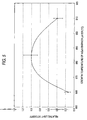
- Fig. 1 The relationship between the thickness of InGaN layer which is a well layer and the light intensity of the light-emitting device at 20 mA is shown in Fig. 1 (The light intensity of the light-emitting device will hereinafter represent the light intensity of the light-emitting device measured under the application of 20 mA unless otherwise specified).
- the results of Fig. 1 were obtained when the thickness of three InGaN layers constituting the light-emitting layer in the light-emitting device 1 shown in the examples (see Figs. 7 and 8) were varied as in the abscissa.
- the thickness of InGaN layer is preferably from 35 to 50 angstrom (3.5 to 5.0 nm), more preferably from 37 to 48 angstrom (3.7 to 4.8 nm), even more preferably from 40 to 45 angstrom (4.0 to 4.5 nm).
- Fig. 2 The relationship between the growth rate of InGaN layer and the light emission intensity of the light-emitting device is shown in Fig. 2.
- Fig. 2 The results of Fig. 2 were obtained when the growth rate of InGaN layer constituting the light-emitting layer in the light-emitting device shown in the examples was varied as in the abscissa.
- the growth rate of InGaN layer is preferably from 0.2 to 0.7 angstrom/s (0.02 to 0.07 nm/s).
- the growth rate of InGaN layer is more preferably from 0.25 to 0.6 angstrom/s (0.025 to 0.06 nm/s), even more preferably from 0.35 to 0.5 angstrom/s (0.035 to 0.05 nm/s).
- the growth rate was controlled by varying the flow rate of material gases (TMG, TMI, ammonia).
- Fig. 3 The results of Fig. 3 were obtained when the growth temperature of InGaN layer constituting the light-emitting layer in the light-emitting device shown in the examples was varied as in the abscissa.
- the growth temperature of InGaN layer be preferably 850°C or lower, more preferably 840°C or lower.
- the lower limit of the growth temperature of InGaN layer is not specifically limited so far as InGaN layer can grow.
- Fig. 4 The relationship between the thickness of AlGaN layer which is a barrier layer and the light emission intensity of the light-emitting device is shown in Fig. 4.
- the results of Fig. 4 were obtained when the thickness of four AlGaN layers constituting the light-emitting layer in the light-emitting device shown in the examples were varied as in the abscissa.
- the thickness of AlGaN layer be preferably 50 angstrom (5.0 nm) or more, more preferably 60 angstrom (6.0 nm) or more, even more preferably 70 angstrom (7.0 nm) or more.
- the upper limit of AlGaN layer is not specifically limited but is preferably from 100 to 500 angstrom (10 to 50 nm) from the standpoint of production step, etc.
- the AlGaN layer disposed closest to the p-type contact layer acts as a cap layer and thus is preferably formed 10 to 30% thicker than the other AlGaN layers.
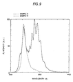
- Fig. 9 illustrate PL spectrum developed when a laminate according to the embodiment shown in Fig. 7 (buffer layer was formed at a low temperature) was irradiated with He-Cd laser beam.
- Sample A shown by the solid line indicates the case where the thickness of one unit pair is 16 nm (160 angstrom) and Sample B shown by the broken line indicates the case where the thickness of one unit pair is 8. nm (80 angstrom).
- Sample B showed little emission of light having a wavelength attributed to the light-emitting layer (385 nm or more) while Sample A showed a strong emission of light at this wavelength.
- the emission of light in the vicinity of 370 nm is attributed to GaN layer of the element.
- the thickness of one unit pair is preferably 10 nm or more, more preferably from 10 to 100 nm, even more preferably from 10 to 50 nm, further even more preferably from 10 to 20 nm.
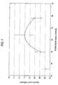
- the thickness of the well layer and the barrier layer are each not specifically limited, but the results of Fig. 7 were obtained by keeping the ratio of thickness of well layer to thickness of barrier layer to about 3 : 7.
- the reason why as the thickness of the well layer and the barrier layer increase, the light emission intensity increases is considered as follows. In other words, since the thickness of the barrier layer increases, carrier leakage can be prevented and the diffusion of Mg from the p-layer side can be prevented. Further, as the thickness of the well layer increases to some extent, carriers can be sufficiently confined. As the total thickness of these layers increases, the crystallinity of the light-emitting layer is enhanced.
- a further aspect of the present invention focuses on the interlayer made of AlGaN which is a primary coat for the light-emitting layer.
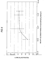
- Fig. 5 The results of Fig. 5 were obtained when the growth temperature of AlGaN interlayer (first interlayer) which is a primary coat for the light-emitting layer was varied as in the abscissa.
- the growth temperature of AlGaN interlayer is preferably from 865 to 905°C, more preferably from 870 to 900°C, even more preferably from 880 to 890°C.
- the impurity concentration of AlGaN interlayer is preferably 2 x 10 16 /cm 3 or more, more preferably 1 x 10 17 /cm 3 .
- the upper limit of the impurity concentration is not specifically limited but is preferably 1 x 10 19 /cm 3 or less.
- AlGaN interlayer was doped with Si as an impurity.
- the thickness of AlGaN interlayer is not specifically limited but is preferably from 100 to 300 nm.
- the semiconductor laminated structure of a light-emitting diode 1 of the embodiment is shown in Fig. 7.
- the carrier concentration is as follows.
- the carrier concentration in the p-type contact layer 17 is 1 x 10 17 /cm 3 or more.
- the carrier concentration in the p-type clad layer 16 is from 0.5.to 2.0 x 10 17 /cm 3 .
- the carrier concentration in the interlayer 14 is 2.0 x 10 18 /cm 3 or more.
- the carrier concentration in the n-type contact layer 13 is 1.0 x 10 18 /cm 3 or more.
- the substrate temperature (growth temperature) was 1,000°C or higher for n-type contact layer 13, p-type clad layer 16 and p-type contact layer 17.
- As the buffer layer there may be used a so-called low temperature buffer layer as well, but a high temperature buffer layer is used in the present example (see Japanese Patent Publication No. JP 2001-15443A).
- the substrate 11 of the aforementioned light-emitting diode 1 is formed by sapphire, but the present invention is not limited thereto.
- the substrate material include spinel (MgAl 2 O 4 ), SiC (including 6H, 4H, 3C), zinc oxide (ZnO), zinc sulfide (ZnS), magnesium oxide, group III nitride compound semiconductor single crystal (GaAs, GaP, etc.), and silicon (Si).
- the light-emitting diode having the aforementioned arrangement is produced in the following manner.
- said sapphire substrate 11 is heated to 1,130°C in the stream of a hydrogen gas through the reactor in MOCVD device to clean the surface thereof ( a plane).
- TMA and NH 3 are introduced into the reactor at that substrate temperature to allow a buffer layer 12 made of AlN to grow in MOCVD method.
- n-type contact layer 13 is formed with the substrate temperature being kept at 1,130°C.
- group III nitride compound semiconductor layers 14 to 17 are formed according to an ordinary method (MOCVD method).
- ammonia gas and gas of alkylated group III compound such as trimethyl gallium (TMG), trimethyl aluminum (TMA) and trimethyl indium (TMI) are supplied onto a substrate which has been heated to a proper temperature to undergo pyrolysis reaction, thereby allowing a desired crystal to grow on the substrate.
- alkylated group III compound such as trimethyl gallium (TMG), trimethyl aluminum (TMA) and trimethyl indium (TMI) are supplied onto a substrate which has been heated to a proper temperature to undergo pyrolysis reaction, thereby allowing a desired crystal to grow on the substrate.
- silane or disilane to introduce silicon into the substrate.
- an impurity there is used (RC 5 H 4 ) 2 Mg to introduce magnesium (Mg) into the substrate As an impurity there is used (RC 5 H 4 ) 2 Mg to introduce magnesium (Mg) into the substrate.
- the substrate temperature at which the first interlayer 14 is allowed to grow is preferably from 865 to 905°C (see Fig. 5) and is 885°C in the present example.
- the substrate temperature at which InGaN layer 15b in the light-emitting layer 15 is allowed to grow is preferably 850°C or lower as shown in Fig. 3 and is 840°C in the present example.
- the growth temperature of AlGaN layer 15a in the light-emitting layer 15 is not specifically limited so far as the well layer containing indium (In) doesn't disappear, but the substrate temperature is 885°C in the present example.
- the substrate temperature of p-type clad layer 16 and p-type contact layer were kept at 1,000°C.
- the semiconductor layer is partly removed by ion etching with Ti/Ni as a mask to expose the n-type contact layer 13 on which an n-electrode pad 21 is to form (see Fig. 8).
- a photoresist is then uniformly applied to the surface of the semiconductor.
- the semiconductor is then subjected to photolithography to remove the photoresist from the p-type contact layer 17 at the area where the electrode is formed so that the p-type contact layer 17 is exposed at that area.
- an Au-Co light-transmitting electrode layer 19 is formed on the p-type contact layer 17 thus exposed.
- a p-electrode pad 20 and an n-electrode pad 21 are vacuum-deposited similarly.
- the light-emitting diode thus arranged was able to emit light having a wavelength of 382 nm.
- a group III nitride compound semiconductor light-emitting device comprising a light-emitting layer having a portion where an InGaN layer is interposed between AlGaN layers on both sides thereof is disclosed.
- the thickness of InGaN layer may be predetermined to a range of from 3.5 to 5 nm.
- the thickness of AlGaN layer may be predetermined to 5 nm or more.
- InGaN layer may be formed at a growth rate of from 0.02 to 0.07 nm/s. Further, InGaN layer may be formed at a growth temperature of 850°C or lower.
- the thickness of InGaN layer, thickness of AlGaN layer, growth rate of InGaN layer and growth rate of InGaN layer may be applied in arbitrary combination.
- the light-emitting layer may comprise one or more unit pairs each comprising a laminate of said AlGaN layer and said InGaN layer and said AlGaN layer laminated thereon as an outermost layer.
- the light-emitting device may comprise an interlayer made of AlGaN having a growth temperature of from 865 to 905°C and/or an impurity concentration of 2 x 10 16 /cm 3 or more and said light-emitting layer formed on said interlayer.
- a process for the production of a group III nitride compound semiconductor light-emitting device comprising a light-emitting layer having a portion where an InGaN layer is interposed between AlGaN layers on both sides thereof is disclosed and said process employs any of (i) step of forming InGaN layer at a growth rate of from 0.02 to 0.07 nm/s, (ii) step of forming InGaN layer at a growth temperature of 850°C or lower and (iii) step of forming an interlayer made of AlGaN at a growth temperature of from 865 to 905°C before the formation of interlayer.
- steps (i) to (iii) may be applied in arbitrary combination.
- the light-emitting layer may comprise one or more unit pairs each comprising a laminate of said AlGaN layer and said InGaN layer and said AlGaN layer laminated thereon as an outermost layer.
- the light-emitting layer may be formed so as to emit light having a wavelength of from 360 to 550 nm or from 360 to 430 nm.
- the thickness of the aforementioned InGaN layer may be predetermined to a range of from 3.5 to 5 nm and the thickness of the aforementioned AlGaN layer may be predetermined to 5 nm or more.
- the aforementioned interlayer may have an impurity concentration of 2 x 10 16 /cm 3 or more.
- a laminate for group III nitride compound semiconductor light-emitting device which emits light having a wavelength of from 360 to 550 nm, comprising a light-emitting layer having a portion where an InGaN layer is interposed between AlGaN layers on both sides thereof, is disclosed.
- the thickness of InGaN layer may be predetermined to a range of from 3.5 to 5 nm.
- the thickness of AlGaN layer may be predetermined to 5 nm or more.
- InGaN layer may be formed at a growth rate of from 0.02 to 0.07 nm/s. Further, InGaN layer may be formed at a growth temperature of 850°C or lower.
- the thickness of InGaN layer, thickness of AlGaN layer, growth rate of InGaN layer and growth rate of InGaN layer may be applied in arbitrary combination.
- the light-emitting layer may comprise one or more unit pairs each comprising a laminate of said AlGaN layer and said InGaN layer and said AlGaN layer laminated thereon as an outermost layer.
- the light-emitting device may comprise an interlayer made of AlGaN having a growth temperature of from 865 to 905°C and/or an impurity concentration of 2 x 10 16 /cm 3 or more and said light-emitting layer formed on said interlayer.
- a laminate which emits light having a wavelength of from 360 to 550 nm or from 360 to 430 nm from a light-emitting layer, comprising an interlayer made of AlGaN having a growth temperature of from 865 to 905°C and/or an impurity concentration of 2 x 10 16 /cm 3 or more and said light-emitting layer formed on said interlayer, is disclosed.
- a laminate comprising a light-emitting layer having a portion where an InGaN layer is interposed between AlGaN layers on both sides thereof is disclosed.
- the thickness of InGaN layer may be predetermined to a range of from 3.5 to 5 nm.
- the thickness of AlGaN layer may be predetermined to 5 nm or more.
- InGaN layer may be formed at a growth rate of from 0.02 to 0.07 nm/s.
- InGaN layer may be formed at a growth temperature of 850°C or lower.
- the thickness of InGaN layer, thickness of AlGaN layer, growth rate of InGaN layer and growth rate of INGaN layer may be applied in arbitrary combination.
- the light-emitting layer may comprise one or more unit pairs each comprising a laminate of said AlGaN layer and said InGaN layer and said AlGaN layer laminated thereon as an outermost layer.
- the light-emitting device may comprise an interlayer made of AlGaN having a growth temperature of from 865 to 905°C and/or an impurity concentration of 2 x 10 16 /cm 3 or more and said light-emitting layer formed on said interlayer.
- a process for the production of a laminate comprising a light-emitting layer having a portion where an InGaN layer is interposed between AlGaN layers on both sides thereof is disclosed and said process employs any of (i) step of forming InGaN layer at a growth rate of from 0.02 to 0.07 nm/s, (ii) step of forming InGaN layer at a growth temperature of 850°C or lower and (iii) step of forming an interlayer made of AlGaN at a'growth temperature of from 865 to 905°C before the formation of interlayer.
- steps (i) to (iii) may be applied in arbitrary combination.
- the light-emitting layer may comprise one or more unit pairs each comprising a laminate of said AlGaN layer and said InGaN layer and said AlGaN layer laminated thereon as an outermost layer.
- the light-emitting layer may be formed so as to emit light having a wavelength of from 360 to 550 nm or from 360 to 430 nm.
- the thickness of the aforementioned InGaN layer may be predetermined to a range of from 3.5 to 5 nm and the thickness of the aforementioned AlGaN layer may be predetermined to 5 nm or more.
- the aforementioned interlayer may have an impurity concentration of 2 x 10 16 /cm 3 or more.
- a group III nitride compound semiconductor light-emitting device which emits light having a wavelength of from 360 t 550 nm, comprising a light-emitting layer having a portion where an InGaN layer is interposed between AlGaN layers on both sides thereof wherein the sum of the thickness of one said InGaN layer and one said AlGaN layer laminated continuously on said InGaN layer is 10 nm or more,: is disclosed.
- the thickness of InGaN layer may be predetermined to a range of from 3.5 to 5 nm.
- the thickness of AlGaN layer may be predetermined to 5 nm or more.
- InGaN layer may be formed at a growth rate of from 0.02 to 0.07 nm/s. Further, InGaN layer may be formed at a growth temperature of 850°C or lower.
- the thickness of InGaN layer, thickness of AlGaN layer, growth rate of InGaN layer and growth rate of InGaN layer may be applied in arbitrary combination.
- the light-emitting layer may comprise one or more unit pairs each comprising a laminate of said AlGaN layer and said InGaN layer and said AlGaN layer laminated thereon as an outermost layer.
- the light-emitting device may comprise an interlayer made of AlGaN having a growth temperature of from 865 to 905°C and/or an impurity concentration of 2 x 10 16 /cm 3 or more and said light-emitting layer formed on said interlayer.
- a group III nitride compound semiconductor light-emitting device comprising a light-emitting layer having a portion where an InGaN layer is interposed between AlGaN layers on both sides thereof wherein the sum of the thickness of one said InGaN layer and one said AlGaN layer laminated continuously on said InGaN layer is 10 nm or more is disclosed.
- the thickness of InGaN layer may be predetermined to a range of from 3.5 to 5 nm.
- the thickness of AlGaN layer may be predetermined to 5 nm or more.
- InGaN layer may be formed at a growth rate of from 0.02 to 0.07 nm/s.
- InGaN layer may be formed at a growth temperature of 850°C or lower.
- the thickness of InGaN layer, thickness of AlGaN layer, growth rate of InGaN layer and growth rate of InGaN layer may be applied in arbitrary combination.
- the light-emitting layer may comprise one or more unit pairs each comprising a laminate of said AlGaN layer and said InGaN layer and said AlGaN layer laminated thereon as an outermost layer.
- the light-emitting device may comprise an interlayer made of AlGaN having a growth temperature of from 865 to 905°C and/or an impurity concentration of 2 x 10 16 /cm 3 or more and said light-emitting layer formed on said interlayer.
- a laminate for group III nitride compound semiconductor light-emitting device which emits light having a wavelength of from 360 t 550 nm, comprising a light-emitting layer having a portion where an InGaN layer is interposed between AlGaN layers on both sides thereof wherein the sum of the thickness of one said InGaN layer and one said AlGaN layer laminated continuously on said InGaN layer is 10 nm or more, is disclosed.
- the thickness of InGaN layer may be predetermined to a range of from 3.5 to 5 nm.
- the thickness of AlGaN layer may be predetermined to 5 nm or more.
- InGaN layer may be formed at a growth rate of from 0.02 to 0.07 nm/s. Further, InGaN layer may be formed at a growth temperature of 850°C or lower.
- the thickness of InGaN layer, thickness of AlGaN layer, growth rate of InGaN layer and growth rate of InGaN layer may be applied in arbitrary combination.
- the light-emitting layer may comprise one or more unit pairs each comprising a laminate of said AlGaN layer and said InGaN layer and said AlGaN layer laminated thereon as an outermost layer.
- the light-emitting device may comprise an interlayer made of AlGaN having a growth temperature of from 865 to 905°C and/or an impurity concentration of 2 x 10 16 /cm 3 or more and said light-emitting layer formed on said interlayer.
- a laminate for group III nitride compound semiconductor light-emitting device comprising a light-emitting layer having a portion where an InGaN layer is interposed between AlGaN layers on both sides thereof wherein the sum of the thickness of one said InGaN layer and one said AlGaN layer laminated continuously on said InGaN layer is 10 nm or more is disclosed.
- the thickness of InGaN layer may be predetermined to a range of from 3.5 to 5 nm.
- the thickness of AlGaN layer may be predetermined to 5 nm or more.
- InGaN layer may be formed at a growth rate of from 0.02 to 0.07 nm/s.
- InGaN layer may be formed at a growth temperature of 850°C or lower.
- the thickness of InGaN layer, thickness of AlGaN layer, growth rate of InGaN layer and growth rate of InGaN layer may be applied in arbitrary combination.
- the light-emitting layer may comprise one or more unit pairs each comprising a laminate of said AlGaN layer and said InGaN layer and said AlGaN layer laminated thereon as an outermost layer.
- the light-emitting device may comprise an interlayer made of AlGaN having a growth temperature of from 865 to 905°C and/or an impurity concentration of 2 x 10 16 /cm 3 or more and said light-emitting layer formed on said interlayer.
Landscapes
- Chemical & Material Sciences (AREA)
- Engineering & Computer Science (AREA)
- Nanotechnology (AREA)
- Physics & Mathematics (AREA)
- Life Sciences & Earth Sciences (AREA)
- Biophysics (AREA)
- Optics & Photonics (AREA)
- Crystallography & Structural Chemistry (AREA)
- Led Devices (AREA)
- Semiconductor Lasers (AREA)
Abstract
Description
Claims (32)
- A group III nitride compound semiconductor light-emitting device which emits light having a wavelength of from 360 nm to 550 nm, comprising a light-emitting layer having a portion where an InGaN layer is interposed between AlGaN layers on both sides thereof.
- The group III nitride compound semiconductor light-emitting device as described in Claim 1, wherein the thickness of said InGaN layer is in a range from 3.5 nm to 5 nm.
- The group III nitride compound semiconductor light-emitting device as described in Claim 1, wherein the thickness of said AlGaN layer is 5 nm or more.
- The group III nitride compound semiconductor light-emitting device as described in Claim 1, wherein said InGaN layer has been formed at a growth rate of from 0.02 to 0.07 nm/s.
- The group III nitride compound semiconductor light-emitting device as described in Claim 1, wherein said InGaN layer has been formed at a growth temperature of 850°C or lower.
- The group III nitride compound semiconductor light-emitting device as described in Claim 1, wherein the thickness of said InGaN layer is in a range from 3.5 nm to 5 nm and the thickness of said AlGaN layer is 5 nm or more.
- The group III nitride compound semiconductor light-emitting device as described in Claim 1, wherein the thickness of said InGaN layer is in a range from 3.5 to 5 nm and said InGaN layer has been formed at a growth rate of from 0.02 to 0.07 nm/s.
- The group III nitride compound semiconductor light-emitting device as described in Claim 1, wherein the thickness of said InGaN layer is in a range from 3.5 to 5 nm and said InGaN layer has been formed at a growth temperature of 850°C or lower.
- The group III nitride compound semiconductor light-emitting device as described in Claim 1, wherein the thickness of said AlGaN layer is 5 nm or more and said InGaN layer has been formed at a growth rate of from 0.02 to 0.07 nm/s.
- The group III nitride compound semiconductor light-emitting device as described in Claim 1, wherein the thickness of said AlGaN layer is 5 nm or more and said InGaN layer has been formed at a growth temperature of 850°C or lower.
- The group III nitride compound semiconductor light-emitting device as described in Claim 1, wherein said InGaN layer has been formed at a growth rate of from 0.02 to 0.07 nm/s and said InGaN layer has been formed at a growth temperature of 850°C or lower.
- The group III nitride compound semiconductor light-emitting device as described in Claim 1, wherein the thickness of said InGaN layer is in a range from 3.5 to 5 nm, the thickness of said AlGaN layer is 5 nm or more, and said InGaN layer has been formed at a growth rate of from 0.02 to 0.07 nm/s.
- The group III nitride compound semiconductor light-emitting device as described in Claim 1, wherein the thickness of said InGaN layer is in a range from 3.5 to 5 nm, the thickness of said AlGaN layer is 5 nm or more, and said InGaN layer has been formed at a growth temperature of 850°C or lower.
- The group III nitride compound semiconductor light-emitting device as described in Claim 1, wherein the thickness of said AlGaN layer is 5 nm or more, said InGaN layer has been formed at a growth rate of from 0.02 to 0.07 nm/s, and said InGaN layer has been formed at a growth temperature of 850°C or lower.
- The group III nitride compound semiconductor light-emitting device as described in Claim 1, wherein the thickness of said InGaN layer is in a range from 3.5 to 5 nm, said InGaN layer has been formed at a growth rate of from 0.02 to 0.07 nm/s, and said InGaN layer has been formed at a growth temperature of 850°C or lower.
- The group III nitride compound semiconductor light-emitting device as described in Claim 1, wherein the thickness of said InGaN layer is in a range from 3.5 to 5 nm, the thickness of said AlGaN layer is 5 nm or more, said InGaN layer has been formed at a growth rate of from 0.02 to 0.07 nm/s and said InGaN layer has been formed at a growth temperature of 850°C or lower.
- The group III nitride compound semiconductor light-emitting device as described in Claim 1, wherein said light-emitting layer comprises one or more unit pairs each comprising a laminate of said AlGaN layer and said InGaN layer and said AlGaN layer laminated thereon as an outermost layer.
- The group III nitride compound semiconductor light-emitting device as described in Claim 1, wherein the wavelength of light emitted is in a range from 360 to 430 nm.
- The group III nitride compound semiconductor light-emitting device as described in Claim 1, wherein said light-emitting layer comprises one or more unit pairs each comprising a laminate of said AlGaN layer and said InGaN layer and said AlGaN layer laminated thereon as an outermost layer and the wavelength of light emitted is in a range from 360 to. 430 nm.
- The group III nitride compound semiconductor light-emitting device as described in Claim 1, further comprising an interlayer disposed adjacent to said light-emitting layer and made of AlGaN having a growth temperature of from 865 to 905°C.
- The group III nitride compound semiconductor light-emitting device as described in Claim 1, further comprising an interlayer disposed adjacent to said light-emitting layer and made of AlGaN having an impurity concentration of 2 x 10¹⁶/cm3 or more.
- The group III nitride compound semiconductor light-emitting device as described in Claim 1, further comprising an interlayer disposed adjacent to said light-emitting layer and made of AlGaN having a growth temperature of from 865 to 905°C and an impurity concentration of 2 x 10¹⁶/cm3 or more.
- A group III nitride compound semiconductor light-emitting device comprising an interlayer made of AlGaN having a growth temperature of from 865 to 905°C and a light-emitting layer formed on said interlayer which emits light having a wavelength of from 360 to 550 nm from said light-emitting layer.
- The group III nitride compound semiconductor light-emitting device as described in Claim 23, wherein said wavelength is in a range from 360 to 430 nm.
- A group III nitride compound semiconductor light-emitting device comprising an interlayer made of AlGaN having an impurity concentration of 2 x 10¹⁶/cm3 or more and a light-emitting layer formed on said interlayer which emits light having a wavelength of from 360 to 550 nm from said light-emitting layer.
- The group III nitride compound semiconductor light-emitting device as described in Claim 25, wherein said wavelength is in a range from 360 to 430 nm.
- A group III nitride compound semiconductor light-emitting device comprising an interlayer made :of AlGaN having a growth temperature of from 865 to 905°C and an impurity concentration of 2 x 10¹⁶/cm3 or more and a light-emitting layer formed on said interlayer which emits light having a wavelength of from 360 to 550 nm from said light-emitting layer.
- The group III nitride compound semiconductor light-emitting device as described in Claim 27, wherein said wavelength is a ranges from 360 to 430 nm.
- A group III nitride compound semiconductor light-emitting device which emits light having a wavelength of from 360 to 550 nm, comprising a light-emitting layer having a portion where an InGaN layer is interposed between AlGaN layers on both sides thereof wherein the sum of the thickness of one said InGaN layer and one said AlGaN layer laminated continuously on said InGaN layer is 10 nm or more.
- The group III nitride compound semiconductor light-emitting device as described in Claim 29, wherein said InGaN layer has been formed at a growth rate of from 0.02 to 0.07 nm/s.
- The group III nitride compound semiconductor light-emitting device as described in Claim 29, wherein said InGaN layer has been formed at a growth temperature of 850°C or lower.
- The group III nitride compound semiconductor light-emitting device as described in Claim 29, wherein said InGaN layer has been formed at a growth rate of from 0.02 to 0.07 nm/s and said InGaN layer has been formed at a growth temperature of 850°C or lower.
Applications Claiming Priority (5)
| Application Number | Priority Date | Filing Date | Title |
|---|---|---|---|
| JP2000201563 | 2000-07-03 | ||
| JP2000201563 | 2000-07-03 | ||
| JP2000323231 | 2000-10-23 | ||
| JP2000323231A JP2002084000A (en) | 2000-07-03 | 2000-10-23 | Group III nitride compound semiconductor light emitting device |
| PCT/JP2001/005769 WO2002003517A1 (en) | 2000-07-03 | 2001-07-03 | Iii group nitride compound semiconductor light emitting element |
Publications (2)
| Publication Number | Publication Date |
|---|---|
| EP1306946A1 true EP1306946A1 (en) | 2003-05-02 |
| EP1306946A4 EP1306946A4 (en) | 2004-12-29 |
Family
ID=26595293
Family Applications (1)
| Application Number | Title | Priority Date | Filing Date |
|---|---|---|---|
| EP01945803A Ceased EP1306946A4 (en) | 2000-07-03 | 2001-07-03 | SEMICONDUCTOR LIGHTING PASSION WITH GROUP III NITRIDE CONNECTION |
Country Status (8)
| Country | Link |
|---|---|
| US (1) | US6838706B2 (en) |
| EP (1) | EP1306946A4 (en) |
| JP (1) | JP2002084000A (en) |
| KR (2) | KR20030011147A (en) |
| CN (1) | CN1286230C (en) |
| AU (1) | AU2001267920A1 (en) |
| TW (1) | TWI242297B (en) |
| WO (1) | WO2002003517A1 (en) |
Families Citing this family (22)
| Publication number | Priority date | Publication date | Assignee | Title |
|---|---|---|---|---|
| JP2002084000A (en) | 2000-07-03 | 2002-03-22 | Toyoda Gosei Co Ltd | Group III nitride compound semiconductor light emitting device |
| GB2407702A (en) * | 2003-10-28 | 2005-05-04 | Sharp Kk | A semiconductor light-emitting device |
| WO2005086243A1 (en) * | 2004-03-08 | 2005-09-15 | Showa Denko K.K. | Pn junction type croup iii nitride semiconductor light-emitting device |
| KR100770491B1 (en) * | 2005-03-16 | 2007-10-25 | 최운용 | Fabrication of Optical Semiconductor Transparent Electrode by Plasma Treatment |
| JP2006332365A (en) * | 2005-05-26 | 2006-12-07 | Toyoda Gosei Co Ltd | Group III nitride compound semiconductor light emitting device and light emitting device using the same |
| JP5025168B2 (en) * | 2006-06-08 | 2012-09-12 | 昭和電工株式会社 | Method for producing group III nitride semiconductor multilayer structure |
| JP2010536182A (en) * | 2007-08-08 | 2010-11-25 | ザ リージェンツ オブ ザ ユニバーシティ オブ カリフォルニア | Nonpolar III-nitride light emitting diodes with long wavelength radiation |
| KR100972978B1 (en) * | 2007-12-13 | 2010-07-29 | 삼성엘이디 주식회사 | Nitride semiconductor devices |
| JP4640427B2 (en) * | 2008-03-14 | 2011-03-02 | ソニー株式会社 | GaN-based semiconductor light-emitting device, light-emitting device assembly, light-emitting device, method for manufacturing GaN-based semiconductor light-emitting device, driving method for GaN-based semiconductor light-emitting device, and image display device |
| JP4908453B2 (en) * | 2008-04-25 | 2012-04-04 | 住友電気工業株式会社 | Method for fabricating a nitride semiconductor laser |
| JP5196160B2 (en) * | 2008-10-17 | 2013-05-15 | 日亜化学工業株式会社 | Semiconductor light emitting device |
| JP5353802B2 (en) * | 2010-04-12 | 2013-11-27 | 豊田合成株式会社 | Semiconductor light emitting device manufacturing method, lamp, electronic device, and mechanical device |
| JP2012169383A (en) * | 2011-02-11 | 2012-09-06 | Toyoda Gosei Co Ltd | Group iii nitride semiconductor light-emitting element and method of manufacturing the same |
| JP2013008803A (en) * | 2011-06-23 | 2013-01-10 | Toyoda Gosei Co Ltd | Method for manufacturing group iii nitride semiconductor light-emitting element |
| TWI524551B (en) | 2012-11-19 | 2016-03-01 | 新世紀光電股份有限公司 | Nitride semiconductor structure and semiconductor light emitting device |
| CN107482097A (en) * | 2013-01-25 | 2017-12-15 | 新世纪光电股份有限公司 | Nitride semiconductor structure and semiconductor light emitting element |
| JP6415909B2 (en) | 2014-09-17 | 2018-10-31 | 住友化学株式会社 | Manufacturing method of nitride semiconductor template |
| JP6436694B2 (en) | 2014-09-17 | 2018-12-12 | 住友化学株式会社 | Manufacturing method of nitride semiconductor template |
| KR102358689B1 (en) * | 2015-08-26 | 2022-02-04 | 쑤저우 레킨 세미컨덕터 컴퍼니 리미티드 | Light emitting device |
| TWI738640B (en) * | 2016-03-08 | 2021-09-11 | 新世紀光電股份有限公司 | Semiconductor structure |
| TWI717386B (en) | 2016-09-19 | 2021-02-01 | 新世紀光電股份有限公司 | Semiconductor device containing nitrogen |
| CN111200235A (en) * | 2020-01-10 | 2020-05-26 | 松山湖材料实验室 | Preparation method and device of on-chip integrated AlGaN pulse laser |
Family Cites Families (22)
| Publication number | Priority date | Publication date | Assignee | Title |
|---|---|---|---|---|
| JPH07273366A (en) * | 1994-03-28 | 1995-10-20 | Pioneer Electron Corp | Method for manufacturing group III nitride light emitting device |
| US5557115A (en) | 1994-08-11 | 1996-09-17 | Rohm Co. Ltd. | Light emitting semiconductor device with sub-mount |
| US5751752A (en) | 1994-09-14 | 1998-05-12 | Rohm Co., Ltd. | Semiconductor light emitting device and manufacturing method therefor |
| US5777350A (en) * | 1994-12-02 | 1998-07-07 | Nichia Chemical Industries, Ltd. | Nitride semiconductor light-emitting device |
| EP0772249B1 (en) * | 1995-11-06 | 2006-05-03 | Nichia Corporation | Nitride semiconductor device |
| JPH1012922A (en) * | 1996-06-19 | 1998-01-16 | Toyoda Gosei Co Ltd | Group iii nitride semiconductor light emitting element |
| US5684309A (en) | 1996-07-11 | 1997-11-04 | North Carolina State University | Stacked quantum well aluminum indium gallium nitride light emitting diodes |
| JP3314641B2 (en) * | 1996-11-29 | 2002-08-12 | 日亜化学工業株式会社 | Nitride semiconductor laser device |
| JP3904709B2 (en) * | 1997-02-21 | 2007-04-11 | 株式会社東芝 | Nitride-based semiconductor light-emitting device and method for manufacturing the same |
| KR19990014304A (en) * | 1997-07-30 | 1999-02-25 | 아사구사 나오유끼 | Semiconductor laser, semiconductor light emitting device and manufacturing method thereof |
| JPH11340580A (en) * | 1997-07-30 | 1999-12-10 | Fujitsu Ltd | Semiconductor laser, semiconductor light emitting device, and method of manufacturing the same |
| JPH11312841A (en) | 1998-04-28 | 1999-11-09 | Nichia Chem Ind Ltd | Nitride semiconductor laser device |
| JPH11330547A (en) | 1998-05-15 | 1999-11-30 | Matsushita Electron Corp | Semiconductor light emitting element and its manufacture |
| JP2000077795A (en) * | 1998-06-17 | 2000-03-14 | Matsushita Electric Ind Co Ltd | Semiconductor laser device |
| US6606335B1 (en) * | 1998-07-14 | 2003-08-12 | Fujitsu Limited | Semiconductor laser, semiconductor device, and their manufacture methods |
| JP3703975B2 (en) * | 1998-09-10 | 2005-10-05 | 豊田合成株式会社 | Gallium nitride compound semiconductor light emitting device |
| JP2000091631A (en) * | 1998-09-10 | 2000-03-31 | Toyoda Gosei Co Ltd | Gallium nitride-based compound semiconductor light emitting element |
| JP2000100735A (en) | 1998-09-25 | 2000-04-07 | Sumitomo Chem Co Ltd | Group 3-5 compound semiconductor |
| JP3399374B2 (en) * | 1998-10-23 | 2003-04-21 | 昭和電工株式会社 | Light emitting device with quantum well structure |
| JP2000286448A (en) * | 1999-03-31 | 2000-10-13 | Toyoda Gosei Co Ltd | Group III nitride compound semiconductor light emitting device |
| JP4465748B2 (en) | 1999-06-30 | 2010-05-19 | 豊田合成株式会社 | Method for producing group III nitride compound semiconductor device |
| JP2002084000A (en) | 2000-07-03 | 2002-03-22 | Toyoda Gosei Co Ltd | Group III nitride compound semiconductor light emitting device |
-
2000
- 2000-10-23 JP JP2000323231A patent/JP2002084000A/en active Pending
-
2001
- 2001-07-03 TW TW090116407A patent/TWI242297B/en not_active IP Right Cessation
- 2001-07-03 EP EP01945803A patent/EP1306946A4/en not_active Ceased
- 2001-07-03 US US10/332,024 patent/US6838706B2/en not_active Expired - Lifetime
- 2001-07-03 KR KR10-2003-7000002A patent/KR20030011147A/en not_active Abandoned
- 2001-07-03 KR KR1020067002958A patent/KR100680430B1/en not_active Expired - Lifetime
- 2001-07-03 WO PCT/JP2001/005769 patent/WO2002003517A1/en not_active Ceased
- 2001-07-03 AU AU2001267920A patent/AU2001267920A1/en not_active Abandoned
- 2001-07-03 CN CN01812310.4A patent/CN1286230C/en not_active Expired - Lifetime
Also Published As
| Publication number | Publication date |
|---|---|
| US20030189218A1 (en) | 2003-10-09 |
| US6838706B2 (en) | 2005-01-04 |
| CN1440578A (en) | 2003-09-03 |
| KR20030011147A (en) | 2003-02-06 |
| CN1286230C (en) | 2006-11-22 |
| EP1306946A4 (en) | 2004-12-29 |
| KR20060022733A (en) | 2006-03-10 |
| TWI242297B (en) | 2005-10-21 |
| AU2001267920A1 (en) | 2002-01-14 |
| WO2002003517A1 (en) | 2002-01-10 |
| JP2002084000A (en) | 2002-03-22 |
| KR100680430B1 (en) | 2007-02-08 |
Similar Documents
| Publication | Publication Date | Title |
|---|---|---|
| US6838706B2 (en) | Group III nitride compound semiconductor light-emitting device which emits light having a wavelength in a range from 360 to 550 NM | |
| US6853009B2 (en) | Light-emitting semiconductor device using gallium nitride compound semiconductor | |
| KR100267839B1 (en) | Nitride semiconductor devices | |
| US6881602B2 (en) | Gallium nitride-based semiconductor light emitting device and method | |
| US7576363B2 (en) | Group III nitride compound semiconductor light emitting device | |
| EP0732754B1 (en) | Light-emitting semiconductor device using group III nitride compound | |
| KR100583334B1 (en) | Group III nitride compound semiconductor light emitting device | |
| US6806571B2 (en) | III nitride compound semiconductor element an electrode forming method | |
| KR20220140749A (en) | Red LEDs and how to make them | |
| KR19980024551A (en) | Semiconductor light emitting device and manufacturing method thereof | |
| JP6641335B2 (en) | Nitride semiconductor light emitting device and method of manufacturing nitride semiconductor light emitting device | |
| KR100752007B1 (en) | Group ? nitride compound semiconductor light-emitting diode and method for manufacturing thereof | |
| US7981775B2 (en) | Nitride semiconductor light-emitting device having high light efficiency and method of manfacturing the same | |
| KR101261629B1 (en) | Method for fabricating a compound semiconductor device | |
| KR101321936B1 (en) | LIGHT EMITTING DIODE HAVING ZnO LAYER P-TYPED AND THE METHOD OF FABRICATING THE LIGHT EMITTING DIODE | |
| JP2005203604A (en) | Nitride-based iii group compound semiconductor light element | |
| US20240297270A1 (en) | Green LED With Current-Invariant Emission Wavelength | |
| KR101259991B1 (en) | Method for fabricating a compound semiconductor device | |
| JP3874779B2 (en) | Ge-doped n-type group III nitride semiconductor layered product, method for producing the same, and group III nitride semiconductor light-emitting device using the same | |
| JP2005183780A (en) | Manufacturing method of nitride-based iii group compound semiconductor light emitting element | |
| JP2004146499A (en) | Method for manufacturing group iii nitride compound semiconductor element |
Legal Events
| Date | Code | Title | Description |
|---|---|---|---|
| PUAI | Public reference made under article 153(3) epc to a published international application that has entered the european phase |
Free format text: ORIGINAL CODE: 0009012 |
|
| 17P | Request for examination filed |
Effective date: 20021231 |
|
| AK | Designated contracting states |
Designated state(s): AT BE CH CY DE DK ES FI FR GB GR IE IT LI LU MC NL PT SE TR |
|
| AX | Request for extension of the european patent |
Extension state: AL LT LV MK RO SI |
|
| RBV | Designated contracting states (corrected) |
Designated state(s): DE FR GB |
|
| A4 | Supplementary search report drawn up and despatched |
Effective date: 20041112 |
|
| RIC1 | Information provided on ipc code assigned before grant |
Ipc: 7H 01S 5/343 B Ipc: 7H 01L 33/00 A |
|
| 17Q | First examination report despatched |
Effective date: 20050222 |
|
| STAA | Information on the status of an ep patent application or granted ep patent |
Free format text: STATUS: THE APPLICATION HAS BEEN REFUSED |
|
| 18R | Application refused |
Effective date: 20070625 |