JP6436694B2 - Manufacturing method of nitride semiconductor template - Google Patents
Manufacturing method of nitride semiconductor template Download PDFInfo
- Publication number
- JP6436694B2 JP6436694B2 JP2014188710A JP2014188710A JP6436694B2 JP 6436694 B2 JP6436694 B2 JP 6436694B2 JP 2014188710 A JP2014188710 A JP 2014188710A JP 2014188710 A JP2014188710 A JP 2014188710A JP 6436694 B2 JP6436694 B2 JP 6436694B2
- Authority
- JP
- Japan
- Prior art keywords
- nitride semiconductor
- layer
- gas
- buffer layer
- sapphire substrate
- Prior art date
- Legal status (The legal status is an assumption and is not a legal conclusion. Google has not performed a legal analysis and makes no representation as to the accuracy of the status listed.)
- Active
Links
Images


Classifications
-
- H—ELECTRICITY
- H01—ELECTRIC ELEMENTS
- H01L—SEMICONDUCTOR DEVICES NOT COVERED BY CLASS H10
- H01L33/00—Semiconductor devices with at least one potential-jump barrier or surface barrier specially adapted for light emission; Processes or apparatus specially adapted for the manufacture or treatment thereof or of parts thereof; Details thereof
- H01L33/005—Processes
- H01L33/0062—Processes for devices with an active region comprising only III-V compounds
- H01L33/0066—Processes for devices with an active region comprising only III-V compounds with a substrate not being a III-V compound
- H01L33/007—Processes for devices with an active region comprising only III-V compounds with a substrate not being a III-V compound comprising nitride compounds
-
- C—CHEMISTRY; METALLURGY
- C23—COATING METALLIC MATERIAL; COATING MATERIAL WITH METALLIC MATERIAL; CHEMICAL SURFACE TREATMENT; DIFFUSION TREATMENT OF METALLIC MATERIAL; COATING BY VACUUM EVAPORATION, BY SPUTTERING, BY ION IMPLANTATION OR BY CHEMICAL VAPOUR DEPOSITION, IN GENERAL; INHIBITING CORROSION OF METALLIC MATERIAL OR INCRUSTATION IN GENERAL
- C23C—COATING METALLIC MATERIAL; COATING MATERIAL WITH METALLIC MATERIAL; SURFACE TREATMENT OF METALLIC MATERIAL BY DIFFUSION INTO THE SURFACE, BY CHEMICAL CONVERSION OR SUBSTITUTION; COATING BY VACUUM EVAPORATION, BY SPUTTERING, BY ION IMPLANTATION OR BY CHEMICAL VAPOUR DEPOSITION, IN GENERAL
- C23C16/00—Chemical coating by decomposition of gaseous compounds, without leaving reaction products of surface material in the coating, i.e. chemical vapour deposition [CVD] processes
- C23C16/22—Chemical coating by decomposition of gaseous compounds, without leaving reaction products of surface material in the coating, i.e. chemical vapour deposition [CVD] processes characterised by the deposition of inorganic material, other than metallic material
- C23C16/30—Deposition of compounds, mixtures or solid solutions, e.g. borides, carbides, nitrides
- C23C16/34—Nitrides
-
- C—CHEMISTRY; METALLURGY
- C30—CRYSTAL GROWTH
- C30B—SINGLE-CRYSTAL GROWTH; UNIDIRECTIONAL SOLIDIFICATION OF EUTECTIC MATERIAL OR UNIDIRECTIONAL DEMIXING OF EUTECTOID MATERIAL; REFINING BY ZONE-MELTING OF MATERIAL; PRODUCTION OF A HOMOGENEOUS POLYCRYSTALLINE MATERIAL WITH DEFINED STRUCTURE; SINGLE CRYSTALS OR HOMOGENEOUS POLYCRYSTALLINE MATERIAL WITH DEFINED STRUCTURE; AFTER-TREATMENT OF SINGLE CRYSTALS OR A HOMOGENEOUS POLYCRYSTALLINE MATERIAL WITH DEFINED STRUCTURE; APPARATUS THEREFOR
- C30B23/00—Single-crystal growth by condensing evaporated or sublimed materials
- C30B23/02—Epitaxial-layer growth
- C30B23/025—Epitaxial-layer growth characterised by the substrate
-
- C—CHEMISTRY; METALLURGY
- C30—CRYSTAL GROWTH
- C30B—SINGLE-CRYSTAL GROWTH; UNIDIRECTIONAL SOLIDIFICATION OF EUTECTIC MATERIAL OR UNIDIRECTIONAL DEMIXING OF EUTECTOID MATERIAL; REFINING BY ZONE-MELTING OF MATERIAL; PRODUCTION OF A HOMOGENEOUS POLYCRYSTALLINE MATERIAL WITH DEFINED STRUCTURE; SINGLE CRYSTALS OR HOMOGENEOUS POLYCRYSTALLINE MATERIAL WITH DEFINED STRUCTURE; AFTER-TREATMENT OF SINGLE CRYSTALS OR A HOMOGENEOUS POLYCRYSTALLINE MATERIAL WITH DEFINED STRUCTURE; APPARATUS THEREFOR
- C30B25/00—Single-crystal growth by chemical reaction of reactive gases, e.g. chemical vapour-deposition growth
- C30B25/02—Epitaxial-layer growth
- C30B25/18—Epitaxial-layer growth characterised by the substrate
- C30B25/186—Epitaxial-layer growth characterised by the substrate being specially pre-treated by, e.g. chemical or physical means
-
- C—CHEMISTRY; METALLURGY
- C30—CRYSTAL GROWTH
- C30B—SINGLE-CRYSTAL GROWTH; UNIDIRECTIONAL SOLIDIFICATION OF EUTECTIC MATERIAL OR UNIDIRECTIONAL DEMIXING OF EUTECTOID MATERIAL; REFINING BY ZONE-MELTING OF MATERIAL; PRODUCTION OF A HOMOGENEOUS POLYCRYSTALLINE MATERIAL WITH DEFINED STRUCTURE; SINGLE CRYSTALS OR HOMOGENEOUS POLYCRYSTALLINE MATERIAL WITH DEFINED STRUCTURE; AFTER-TREATMENT OF SINGLE CRYSTALS OR A HOMOGENEOUS POLYCRYSTALLINE MATERIAL WITH DEFINED STRUCTURE; APPARATUS THEREFOR
- C30B29/00—Single crystals or homogeneous polycrystalline material with defined structure characterised by the material or by their shape
- C30B29/10—Inorganic compounds or compositions
- C30B29/40—AIIIBV compounds wherein A is B, Al, Ga, In or Tl and B is N, P, As, Sb or Bi
- C30B29/403—AIII-nitrides
- C30B29/406—Gallium nitride
-
- H—ELECTRICITY
- H01—ELECTRIC ELEMENTS
- H01L—SEMICONDUCTOR DEVICES NOT COVERED BY CLASS H10
- H01L21/00—Processes or apparatus adapted for the manufacture or treatment of semiconductor or solid state devices or of parts thereof
- H01L21/02—Manufacture or treatment of semiconductor devices or of parts thereof
- H01L21/02104—Forming layers
- H01L21/02365—Forming inorganic semiconducting materials on a substrate
- H01L21/02367—Substrates
- H01L21/0237—Materials
- H01L21/0242—Crystalline insulating materials
-
- H—ELECTRICITY
- H01—ELECTRIC ELEMENTS
- H01L—SEMICONDUCTOR DEVICES NOT COVERED BY CLASS H10
- H01L21/00—Processes or apparatus adapted for the manufacture or treatment of semiconductor or solid state devices or of parts thereof
- H01L21/02—Manufacture or treatment of semiconductor devices or of parts thereof
- H01L21/02104—Forming layers
- H01L21/02365—Forming inorganic semiconducting materials on a substrate
- H01L21/02367—Substrates
- H01L21/02428—Structure
- H01L21/0243—Surface structure
-
- H—ELECTRICITY
- H01—ELECTRIC ELEMENTS
- H01L—SEMICONDUCTOR DEVICES NOT COVERED BY CLASS H10
- H01L21/00—Processes or apparatus adapted for the manufacture or treatment of semiconductor or solid state devices or of parts thereof
- H01L21/02—Manufacture or treatment of semiconductor devices or of parts thereof
- H01L21/02104—Forming layers
- H01L21/02365—Forming inorganic semiconducting materials on a substrate
- H01L21/02367—Substrates
- H01L21/02433—Crystal orientation
-
- H—ELECTRICITY
- H01—ELECTRIC ELEMENTS
- H01L—SEMICONDUCTOR DEVICES NOT COVERED BY CLASS H10
- H01L21/00—Processes or apparatus adapted for the manufacture or treatment of semiconductor or solid state devices or of parts thereof
- H01L21/02—Manufacture or treatment of semiconductor devices or of parts thereof
- H01L21/02104—Forming layers
- H01L21/02365—Forming inorganic semiconducting materials on a substrate
- H01L21/02436—Intermediate layers between substrates and deposited layers
- H01L21/02439—Materials
- H01L21/02455—Group 13/15 materials
- H01L21/02458—Nitrides
-
- H—ELECTRICITY
- H01—ELECTRIC ELEMENTS
- H01L—SEMICONDUCTOR DEVICES NOT COVERED BY CLASS H10
- H01L21/00—Processes or apparatus adapted for the manufacture or treatment of semiconductor or solid state devices or of parts thereof
- H01L21/02—Manufacture or treatment of semiconductor devices or of parts thereof
- H01L21/02104—Forming layers
- H01L21/02365—Forming inorganic semiconducting materials on a substrate
- H01L21/02518—Deposited layers
- H01L21/02521—Materials
- H01L21/02538—Group 13/15 materials
- H01L21/0254—Nitrides
-
- H—ELECTRICITY
- H01—ELECTRIC ELEMENTS
- H01L—SEMICONDUCTOR DEVICES NOT COVERED BY CLASS H10
- H01L21/00—Processes or apparatus adapted for the manufacture or treatment of semiconductor or solid state devices or of parts thereof
- H01L21/02—Manufacture or treatment of semiconductor devices or of parts thereof
- H01L21/02104—Forming layers
- H01L21/02365—Forming inorganic semiconducting materials on a substrate
- H01L21/02518—Deposited layers
- H01L21/0257—Doping during depositing
- H01L21/02573—Conductivity type
- H01L21/02576—N-type
-
- H—ELECTRICITY
- H01—ELECTRIC ELEMENTS
- H01L—SEMICONDUCTOR DEVICES NOT COVERED BY CLASS H10
- H01L21/00—Processes or apparatus adapted for the manufacture or treatment of semiconductor or solid state devices or of parts thereof
- H01L21/02—Manufacture or treatment of semiconductor devices or of parts thereof
- H01L21/02104—Forming layers
- H01L21/02365—Forming inorganic semiconducting materials on a substrate
- H01L21/02612—Formation types
- H01L21/02617—Deposition types
- H01L21/0262—Reduction or decomposition of gaseous compounds, e.g. CVD
-
- H—ELECTRICITY
- H01—ELECTRIC ELEMENTS
- H01L—SEMICONDUCTOR DEVICES NOT COVERED BY CLASS H10
- H01L33/00—Semiconductor devices with at least one potential-jump barrier or surface barrier specially adapted for light emission; Processes or apparatus specially adapted for the manufacture or treatment thereof or of parts thereof; Details thereof
- H01L33/02—Semiconductor devices with at least one potential-jump barrier or surface barrier specially adapted for light emission; Processes or apparatus specially adapted for the manufacture or treatment thereof or of parts thereof; Details thereof characterised by the semiconductor bodies
- H01L33/12—Semiconductor devices with at least one potential-jump barrier or surface barrier specially adapted for light emission; Processes or apparatus specially adapted for the manufacture or treatment thereof or of parts thereof; Details thereof characterised by the semiconductor bodies with a stress relaxation structure, e.g. buffer layer
-
- H—ELECTRICITY
- H01—ELECTRIC ELEMENTS
- H01L—SEMICONDUCTOR DEVICES NOT COVERED BY CLASS H10
- H01L33/00—Semiconductor devices with at least one potential-jump barrier or surface barrier specially adapted for light emission; Processes or apparatus specially adapted for the manufacture or treatment thereof or of parts thereof; Details thereof
- H01L33/02—Semiconductor devices with at least one potential-jump barrier or surface barrier specially adapted for light emission; Processes or apparatus specially adapted for the manufacture or treatment thereof or of parts thereof; Details thereof characterised by the semiconductor bodies
- H01L33/20—Semiconductor devices with at least one potential-jump barrier or surface barrier specially adapted for light emission; Processes or apparatus specially adapted for the manufacture or treatment thereof or of parts thereof; Details thereof characterised by the semiconductor bodies with a particular shape, e.g. curved or truncated substrate
-
- H—ELECTRICITY
- H01—ELECTRIC ELEMENTS
- H01L—SEMICONDUCTOR DEVICES NOT COVERED BY CLASS H10
- H01L33/00—Semiconductor devices with at least one potential-jump barrier or surface barrier specially adapted for light emission; Processes or apparatus specially adapted for the manufacture or treatment thereof or of parts thereof; Details thereof
- H01L33/02—Semiconductor devices with at least one potential-jump barrier or surface barrier specially adapted for light emission; Processes or apparatus specially adapted for the manufacture or treatment thereof or of parts thereof; Details thereof characterised by the semiconductor bodies
- H01L33/26—Materials of the light emitting region
- H01L33/30—Materials of the light emitting region containing only elements of group III and group V of the periodic system
- H01L33/32—Materials of the light emitting region containing only elements of group III and group V of the periodic system containing nitrogen
Description
本発明は、窒化物半導体テンプレートの製造方法に関する。 The present invention relates to a method for manufacturing a nitride semiconductor template.
例えば発光ダイオード(LED)等の窒化物半導体発光素子(以下、単に「発光素子」とも言う。)は、窒化物半導体テンプレート上に、発光素子構造として、例えば窒化ガリウム(GaN)等からなるn型半導体層、発光層、p型半導体層を順次成長させて形成されている。窒化物半導体テンプレートは、例えばサファイア基板上に、バッファ層、窒化物半導体層を順次成長させることで形成されている。このような発光素子では、発光層で生じた光をどれだけ効率よく取り出せるかが重要な課題となっている。すなわち、発光素子の光取り出し効率(発光出力)を向上させることが重要となっている。 For example, a nitride semiconductor light emitting device such as a light emitting diode (LED) (hereinafter also simply referred to as “light emitting device”) is an n-type made of, for example, gallium nitride (GaN) as a light emitting device structure on a nitride semiconductor template. A semiconductor layer, a light emitting layer, and a p-type semiconductor layer are sequentially grown. For example, the nitride semiconductor template is formed by sequentially growing a buffer layer and a nitride semiconductor layer on a sapphire substrate. In such a light emitting element, it is an important issue how efficiently light generated in the light emitting layer can be extracted. That is, it is important to improve the light extraction efficiency (light emission output) of the light emitting element.
そこで、発光素子の光取り出し効率を向上させるため、基板の上面に、円錐状や多角形錐状等の凸部を形成する凹凸加工を施したPSS基板(Patterned Sapphire Substrate)が提案されている(例えば特許文献1参照)。そして、PSS基板上に所定厚さのバッファ層を成長させて形成し、バッファ層上にGaN層等の窒化物半導体層を表面が平坦になるまで成長させて形成することで、窒化物半導体テンプレートが形成されている。このような凹凸加工が施されたPSS基板が用いられた窒化物半導体テンプレート上に、発光層等を成長させて形成された発光素子は、発光素子の内部への光の閉じ込めを低減でき、発光素子の光取り出し効率を向上させることができる。 Therefore, in order to improve the light extraction efficiency of the light emitting element, a PSS substrate (Patterned Sapphire Substrate) is proposed in which a concavo-convex process for forming a convex portion such as a conical shape or a polygonal pyramid shape is provided on the upper surface of the substrate ( For example, see Patent Document 1). Then, a buffer layer having a predetermined thickness is grown and formed on the PSS substrate, and a nitride semiconductor layer such as a GaN layer is grown on the buffer layer until the surface becomes flat, thereby forming a nitride semiconductor template. Is formed. A light-emitting element formed by growing a light-emitting layer or the like on a nitride semiconductor template using a PSS substrate subjected to such uneven processing can reduce light confinement inside the light-emitting element and emit light. The light extraction efficiency of the element can be improved.
また、窒化物半導体テンプレートの基板として、このような凹凸加工が施されたPSS基板が用いられると、基板上に例えばGaN層等の窒化物半導体層を成長させる際、窒化物半導体層の成長の初期段階において、窒化物半導体層の島状成長が促進されることで、窒化物半導体層の結晶中での転位同士の会合を増加させることができ、転位の消滅を増加させることができる。従って、凹凸加工が施されていない平坦なサファイア基板(以下では、平坦基板とも言う。)を用いた場合と比較して、結晶中の転位が少ない窒化物半導体層を形成することができる。すなわち、凹凸加工が施されたサファイア基板が用いられると、窒化物半導体層の結晶性を向上させることができる。 Further, when a PSS substrate with such unevenness is used as a substrate for a nitride semiconductor template, when a nitride semiconductor layer such as a GaN layer is grown on the substrate, the growth of the nitride semiconductor layer is performed. In the initial stage, the island-like growth of the nitride semiconductor layer is promoted, so that the association of dislocations in the crystal of the nitride semiconductor layer can be increased, and the disappearance of dislocations can be increased. Therefore, a nitride semiconductor layer with few dislocations in the crystal can be formed as compared with the case where a flat sapphire substrate (hereinafter also referred to as a flat substrate) that has not been processed with unevenness is used. That is, when a sapphire substrate that has been subjected to unevenness processing is used, the crystallinity of the nitride semiconductor layer can be improved.
しかしながら、窒化物半導体テンプレートの基板として凹凸加工が施されたサファイア基板が用いられると、平坦基板が用いられた場合と比べて、デバイス動作の障害となる表面ピットが発生しやすくなる場合があった。 However, when a sapphire substrate with concavo-convex processing is used as a substrate for a nitride semiconductor template, surface pits that obstruct device operation may be more likely to occur than when a flat substrate is used. .
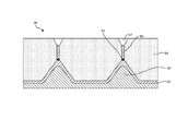
すなわち、サファイア基板の円錐状等の凸部の頂上付近では、凸部の他の箇所と比べて曲率半径が小さい。このため、凸部の頂上や頂上付近には、多数の原子ステップが存在する。凸部が形成された基板上にバッファ層を成長させる際、バッファ層の成長の初期段階においては、基板の凸部の頂上や頂上付近に成長されたバッファ層に多数の原子ステップが残留する。このため、バッファ層の成長が進んでバッファ層の表面が平滑になる(原子ステップがない結晶面となる)までは、凸部の頂上や頂上付近でのバッファ層の成長速度が、他の箇所よりも速くなる傾向にある。従って、バッファ層の成長が進んでバッファ層が厚くなるにつれて、例えば図6に示すように、バッファ層61は、サファイア基板の凸部62の頂上で尖ったような形状に形成されてしまう場合があった。バッファ層61が凸部62の頂上で尖ったような形状に形成されると、凸部62の頂上付近では、表面エネルギが増大し、バッファ層61の成長条件に変調がきたされる。このため、凸部62の頂上付近では、バッファ層61に極性の反転したインバージョンドメイン(ID:Inversion Domain)63が発生し易くなる。バッファ層61にID63が存在すると、バッファ層61上に窒化物半導体層64が成長された場合、バッファ層61のID63上に成長された窒化物半導体層64にもID65が発生する。N極性のID65の成長速度は、IDのないIII族極性(Ga極性など)の窒化物半導体層64の成長速度よりも遅く、ID65上方にピット67が発生する。従って、窒化物半導体層64を厚く成長させても、窒化物半導体層64の表面上、すなわち窒化物半導体テンプレート66の表面上に、ピット67が残留してしまう。
That is, in the vicinity of the top of the convex portion such as a conical shape of the sapphire substrate, the radius of curvature is small compared to other portions of the convex portion. For this reason, there are a large number of atomic steps at the top of the convex portion or near the top. When the buffer layer is grown on the substrate on which the convex portions are formed, in the initial stage of the growth of the buffer layer, many atomic steps remain in the buffer layer grown on the top of the convex portions of the substrate or in the vicinity of the top. For this reason, until the growth of the buffer layer progresses and the surface of the buffer layer becomes smooth (becomes a crystal plane without an atomic step), the growth rate of the buffer layer at the top of the convex portion or near the top is at other locations. Tend to be faster. Therefore, as the growth of the buffer layer proceeds and the buffer layer becomes thicker, for example, as shown in FIG. 6, the
そこで、本発明は、上記課題を解決し、表面ピットの発生を抑制できる窒化物半導体テンプレートの製造方法を提供することを目的とする。 Therefore, an object of the present invention is to provide a method for manufacturing a nitride semiconductor template that solves the above-described problems and can suppress the generation of surface pits.
上記課題を解決するために、本発明は次のように構成されている。
本発明の第1の態様によれば、円錐状又は角錐状の凸部が表面に格子状に配置されて形成されたサファイア基板上に、前記凸部の頂上幅以下で且つ10nm以上330nm以下の厚さにバッファ層を成長させて形成する工程と、前記バッファ層上に窒化物半導体層を成長させて形成する工程と、を有する窒化物半導体テンプレートの製造方法が提供される。
In order to solve the above problems, the present invention is configured as follows.
According to the first aspect of the present invention, on the sapphire substrate formed with conical or pyramidal convex portions arranged in a lattice pattern on the surface, the top width of the convex portions is not more than 10 nm and not more than 330 nm. There is provided a method for manufacturing a nitride semiconductor template, comprising: a step of growing a buffer layer to a thickness; and a step of growing a nitride semiconductor layer on the buffer layer.
本発明の第2の態様によれば、前記バッファ層を形成する工程では、前記バッファ層として、GaN層又はAlN層を600℃以下の温度で成長させる第1の態様の窒化物半導体テンプレートの製造方法が提供される。 According to the second aspect of the present invention, in the step of forming the buffer layer, the nitride semiconductor template according to the first aspect is manufactured by growing a GaN layer or an AlN layer at a temperature of 600 ° C. or less as the buffer layer. A method is provided.
本発明の第3の態様によれば、前記バッファ層を形成する工程では、前記バッファ層として、AlN層を1000℃以上の温度で成長させる第1の態様の窒化物半導体テンプレートの製造方法が提供される。 According to the third aspect of the present invention, in the step of forming the buffer layer, the nitride semiconductor template manufacturing method according to the first aspect is provided in which an AlN layer is grown as the buffer layer at a temperature of 1000 ° C. or higher. Is done.
本発明の第4の態様によれば、前記窒化物半導体層を形成する工程では、前記窒化物半導体層として、GaN層、AlGaN層、InAlGaN層のいずれかを成長させて形成する第1ないし第3の態様のいずれかの窒化物半導体テンプレートの製造方法が提供される。 According to the fourth aspect of the present invention, in the step of forming the nitride semiconductor layer, the nitride semiconductor layer is formed by growing any one of a GaN layer, an AlGaN layer, and an InAlGaN layer. A method for producing a nitride semiconductor template according to any of the three aspects is provided.
本発明の第5の態様によれば、前記バッファ層及び前記窒化物半導体層は、HVPE法又はMOVPE法によって成長される第1ないし第4の態様のいずれかの窒化物半導体テンプレートの製造方法が提供される。 According to a fifth aspect of the present invention, there is provided the nitride semiconductor template manufacturing method according to any one of the first to fourth aspects, wherein the buffer layer and the nitride semiconductor layer are grown by an HVPE method or an MOVPE method. Provided.
本発明にかかる窒化物半導体テンプレートの製造方法によれば、表面ピットの発生を抑制できる。 According to the method for manufacturing a nitride semiconductor template according to the present invention, generation of surface pits can be suppressed.
以下に、本発明の一実施形態にかかる窒化物半導体テンプレート及びこの窒化物半導体テンプレートを用いた半導体発光素子について説明する。 Hereinafter, a nitride semiconductor template and a semiconductor light emitting device using the nitride semiconductor template according to an embodiment of the present invention will be described.
(1)窒化物半導体テンプレート
まず、本実施形態にかかる窒化物半導体テンプレートについて、主に図1及び図2を参照しながら説明する。
(1) Nitride Semiconductor Template First, the nitride semiconductor template according to the present embodiment will be described with reference mainly to FIGS.
図1に示すように、本実施形態にかかる窒化物半導体テンプレート10は、サファイア基板11上に、バッファ層12と、窒化物半導体層13とを順次成長させて構成されている。
As shown in FIG. 1, the
サファイア基板11は、窒化物半導体を成長させる成長面となる、その表面(主面)11aには、図1及び図2に示すように、円錐状又は角錐状(三角錐状、四角錐状、六角錐状など)の凸部14が形成されている。凸部14は、サファイア基板11の表面11aに格子状(三角格子状、正方格子状など)に配置されて形成されている。サファイア基板11の表面11aは、C面とするのが好ましい。凸部14は、例えば、平坦なサファイア基板の表面にフォトリソグラフィ及びドライエッチングにより形成される。
The
凸部14は、図2に示すように、表面11aから凸部14頂上までの高さhを0.3μm以上3μm以下、凸部14底部の幅Dを0.3μm以上4μm以下、隣接する凸部14の底部間の距離Sを0.1μm以上2μm以下、隣接する凸部14,14間のピッチPを0.4μm以上6μm以下とするのが好ましい。また、円錐状又は角錐状の凸部14の頂上幅wは0.01μm以上0.33μm以下とするのが好ましい。
As shown in FIG. 2, the
凸部14が形成されたサファイア基板11として、市販のPSS基板(Patterned Sapphire Substrate)を用いてもよい。また、サファイア基板11は、上面視にて略円形の円形基板でも、あるいは矩形基板などでもよい。
A commercially available PSS substrate (Pattern Sapphire Substrate) may be used as the
このように円錐状又は角錐状の凸部14が格子状に形成されたサファイア基板11を用いることにより、サファイア基板11上に窒化物半導体層13を成長させる際に、窒化物半導体層13の島状成長を促進でき、窒化物半導体層13の結晶中での転位同士の会合による消滅を増加させることができ、窒化物半導体層13の低転位化が図れる。また、窒化物半導体テンプレート10を用いて青色発光ダイオード(青色LED)等の発光素子が形成された場合、発光素子の光取り出し効率を向上せることができる。
When the
凸部14が設けられたサファイア基板11上には、バッファ層12として、例えば窒化ガリウム(GaN)層、窒化アルミニウム(AlN)層等が例えば600℃以下の低温の成長温度で成長されて形成されている。バッファ層12は、例えば1000℃以上の高温の成長温度で成長させたAlN層等であってもよい。
On the
バッファ層12は、凸部14の頂上幅w以下で、且つ10nm以上330nm以下の厚さに形成されている。凸部14の頂上幅wは、凸部14の頂部の曲率半径に関連・関係した長さであり、凸部14の頂部の上方に次第に成長していくバッファ層12の形状を規定するものである。バッファ層12の厚さとしては、凸部14の頂部の上方におけるバッファ層12の厚さ、あるいは凸部14が形成されていないサファイア基板11の表面11a上におけるバッファ層12の厚さとするのがよい。
The
また、上記箇所などの実際のバッファ層12の厚さの測定・管理が難しい場合には、次に示す簡易な方法で、バッファ層12の厚さの形成・管理を行うようにしてもよい。すなわち、凸部14が形成されていない平坦なサファイア基板(以下では、「平坦基板」とも言う。)上に形成したバッファ層(以下では、「平坦バッファ層」とも言う。)の厚さが、凸部14の頂上幅w以下で、10nm以上330nm以下となる成長条件(例えば所定のガスの供給流量及び成長時間等)を求め、この成長条件と同一の成長条件で本実施形態の凸部14が形成されたサファイア基板11上にバッファ層12を成長させて形成する。この場合、平坦なサファイア基板上に成長する平坦バッファ層と、凸部14が形成されたサファイア基板11上に成長するバッファ層12との成長速度の違いを考慮して、上記成長条件を調整するようにしてもよい。
In addition, when it is difficult to measure and manage the actual thickness of the
バッファ層12を上記の厚さとすることにより、窒化物半導体層13の表面ピットの発生を抑制でき、結晶性を向上させることができる。すなわち、バッファ層12の厚さを凸部14の頂上幅w以下とすることにより、あるいは平坦バッファ層の厚さが凸部14の頂上幅w以下となるような成長条件の下で、バッファ層12が成長されて形成されることにより、バッファ層12が、凸部14の頂上部で他の箇所よりも厚く形成され、バッファ層12が凸部14の頂上部で尖ったような形状に形成されてしまうことを抑制できる。これにより、凸部14の頂上や頂上付近に位置する箇所で、バッファ層12にインバージョンドメイン(ID)が発生することを抑制できる。従って、凸部14の頂上や頂上付近の上方の窒化物半導体層13にIDが発生することを抑制できる。その結果、デバイス動作の障害となる窒化物半導体テンプレート10の表面、すなわち窒化物半導体層13の表面にピットが発生することを抑制できる。
By setting the
バッファ層12が、10nm未満の厚さに形成され、あるいは平坦バッファ層の厚さが10nm未満となるような成長条件の下で成長されて形成されると、バッファ層12によるサファイア基板11表面の被覆率が低くなるため、表面ピットの発生を抑制する効果が見られなくなる。一方、バッファ層12の厚さが凸部14の頂上幅w以下であっても、バッファ層12が330nmを超える厚さに形成され、あるいは平坦バッファ層の厚さが330nmを超えるような成長条件の下で成長されて形成されると、バッファ層12自体の結晶品質が低下するため、バッファ層12のIDの発生を抑制できず、窒化物半導体テンプレート10の表面ピットの発生を抑制できない。従って、バッファ層12の厚さは、10nm以上330nm以下の厚さとする。
When the
ここで、凸部14の頂上幅wは、次のように定義した。すなわち、図2に示すように、測定されたサファイア基板11表面の凸部14の外形線(凸部14の頂点を含む縦断面の輪郭線)16における凸部14の高さhの半分の位置(h/2)の点での2つの接線L1,L2(接線L1,L2は点T3で交わる)と、凸部14の外形線16の頂点T0と接し、サファイア基板11の凸部14が形成されていない表面11aと平行である平行線L3とにより形成される三角形T1T2T3の底辺T1T2の長さを凸部14の頂上幅wと定義した。
Here, the top width w of the
図3に示すように、凸部14の外形線16の測定は、原子間力顕微鏡(AFM)により、先鋭化した探針15を用い、探針15を凸部14に沿って移動させることで行われる。凸部14の形状(外形線16)の測定は、例えば、一の凸部14上の複数箇所で探針15の先端の位置情報を読み取り、各情報をそれぞれプロットして行う。凸部14の外形線16の測定には、探針15として、例えば、エッチングにより先端の曲率半径を10nm程度と先鋭化したシリコン製等の探針や、直径が1nm程度であるカーボンナノチューブにより形成された探針を用いるとよい。これにより、サファイア基板11上に形成された凸部14の曲率半径(凸部14の頂上幅w)が小さい場合であっても、凸部14の頂上部(先端)の外形を精密に測定できる。
As shown in FIG. 3, the measurement of the
これに対し、従来のAFM測定やSEM(走査型電子顕微鏡)測定では、nmレベルでの検出が困難な場合があるため、凸部14の頂上部の外形を精密に測定できない場合があった。例えばAFM測定では、探針の先端の曲率半径が通常数100nmであることが多い。このため、図7に示すように、AFM測定では、例えば曲率半径が数100nm程度かそれ以下である凸部14の頂上部を測定しようとすると、図7に実線で示す実際の凸部14の外形よりも大きな、図7に一点鎖線で示すような探針15’の先端形状を反映した外形線16’が観察されてしまう。また、SEM測定では、そもそもサファイア基板11の凸部14の頂上を通る断面を得るのが困難である。
On the other hand, in the conventional AFM measurement and SEM (scanning electron microscope) measurement, it may be difficult to detect at the nm level, and therefore the outer shape of the top of the
図1に示すように、バッファ層12上には、所定厚さ(例えば4μm)の窒化物半導体層13が成長されて形成されている。すなわち、窒化物半導体層13は、その表面が平坦になるまでバッファ層12上に成長されている。窒化物半導体層13として、例えば、窒化ガリウム(GaN)層、窒化ガリウムアルミニウム(AlGaN)層、窒化インジウムアルミニウムガリウム(InAlGaN)層等を成長させるとよい。
As shown in FIG. 1, a
バッファ層12及び窒化物半導体層13は、気相成長法によってサファイア基板11上に成長されて形成されるとよい。気相成長法としては、例えば、ハイドライド気相成長(HVPE:Hydride Vapor Phase Epitaxy)法、有機金属気相成長(MOVPE:Metal−Organic Vapor Phase Epitaxy)法がある。あるいは、分子線エピタキシ(MBE:Molecular Beam Epitaxy)法を用いることができる。特に、HVPE法はサファイア基板11上に結晶を成長させる成長速度が速いため、HVPE法が用いられると、窒化物半導体テンプレート10の製造時間を短くすることができる。従って、製造コストを低減できる。
The
ここで、サファイア基板11上にバッファ層12及び窒化物半導体層13を成長させて形成するハイドライド気相成長装置(HVPE装置)30について図4を用いて説明する。図4は、HVPE装置30の概略構成図を示す。
Here, a hydride vapor phase epitaxy apparatus (HVPE apparatus) 30 for growing the
図4に示すように、HVPE装置30は、例えば石英等により構成される反応炉31を備えている。反応炉31の外周には、反応炉31内を加熱する第1ヒータ32及び第2ヒータ33が設けられている。主に第1ヒータ32によって加熱される反応炉31内の領域は原料部34として機能し、主に第2ヒータ33によって加熱される反応炉31内の領域は成長部35として機能する。原料部34は、第1ヒータ32によって例えば600℃〜900℃に加熱され、後述する反応ガスとガリウム(Ga)又はアルミニウム(Al)とを反応させて原料ガスを生成する空間である。また、成長部35は、第2ヒータ33によって例えば500℃〜1200℃に加熱され、後述する第1のIII族原料ガス供給管40又は第2のIII族原料ガス供給管41から反応炉31内に供給されるIII族原料ガスと、後述するV族原料ガス供給管39から反応炉31内に供給されるV族原料ガスとを反応させ、サファイア基板11上に例えば窒化物半導体層13としてのGaN層を成長させる空間である。なお、第2ヒータ33による加熱温度が成長温度となる。
As shown in FIG. 4, the
反応炉31内の成長部35には、反応炉31内でサファイア基板11を支持する基板支持部としてのサセプタ36が設けられている。サファイア基板11は、成長面がガス供給口に対向するようにサセプタ36上に支持されている。サセプタ36は、例えばカーボンによって構成されており、表面が炭化シリコン(SiC)で覆われている。サセプタ36には、例えば高純度の石英で形成される回転軸37が設けられている。回転軸37が回転されることによって、サセプタ36と共にサファイア基板11が所定の速度(例えば3r/min〜100r/min)で回転するように構成されている。
The
反応炉31には、ドーピングガス供給管38、V族原料ガス供給管39、第1のIII族原料ガス供給管40、第2のIII族原料ガス供給管41がそれぞれ設置されている。ドーピングガス供給管38、V族原料ガス供給管39、第1のIII族原料ガス供給管40、第2のIII族原料ガス供給管41はそれぞれ、例えば高純度の石英で形成されると共に、反応炉31へのガスの供給・停止を行う弁(図示せず)がそれぞれ設けられている。
In the
ドーピングガス供給管38の上流側には、ドーピングガス供給源(図示せず)が接続されている。ドーピングガス供給管38からは、ドーピングガスとして、例えば窒素(N2)ガス、水素(H2)ガス、又はN2ガスとH2ガスとの混合ガス等によって所定濃度(例えば100ppm)に希釈されたジクロロシラン(SiH2Cl2)ガスが反応炉31内の成長部35に供給される。Siドーピング原料ガスとしては、この他、例えば、SiHCl3ガス、SiH3Clガス、SiCl4ガスを用いてもよい。
A doping gas supply source (not shown) is connected to the upstream side of the doping
なお、ドーピングを行わない場合、ドーピングガス供給管38からは、例えばH2ガスや、N2ガス、又はH2ガスとN2ガスとの混合ガスを反応炉31内に供給してもよい。また、ドーピングガス供給管38からは、サファイア基板11に例えば窒化物半導体層13を成長させた後、反応炉31内に付着した付着物等の除去を行うクリーニングガスとして、例えばHClガスや、H2ガス、N2ガス等を反応炉31内に供給してもよい。
When doping is not performed, the doping
V族原料ガス供給管39の上流側には、V族原料ガス供給源(図示せず)が接続されている。V族原料ガス供給管39からは、V族原料ガスとして例えばアンモニア(NH3)ガス等が反応炉31内の成長部35に供給される。
A group V source gas supply source (not shown) is connected to the upstream side of the group V source
V族原料ガス供給管39からは、例えばV族原料ガスと併行して、キャリアガスとしての例えばH2ガス、N2ガス、あるいはこれらの混合ガスを供給してもよい。なお、V族原料ガス供給管39からは、キャリアガスのみを反応炉31内に供給してもよい。
From the V group source
第1のIII族原料ガス供給管40の反応炉31内の原料部34には、Ga(融液)が貯留されるGaタンク42が設置されると共に、第1のIII族原料ガス供給管40の上流側には反応ガス供給源(図示せず)が接続されている。Gaタンク42は、例えば高純度の石英で形成されているとよい。第1のIII族原料ガス供給管40からは、まず、反応ガスとして例えば塩化水素(HCl)ガスがGaタンク42内に供給される。反応ガスがGaタンク42内に供給されることで、III族原料ガスであるGaClガスが生成される。そして、第1のIII族原料ガス供給管40から、反応炉31内の成長部35へGaClガスが供給される。
The
なお、第1のIII族原料ガス供給管40からは、III族原料ガスと併行して、キャリアガスとしての例えばH2ガス、N2ガス、あるいはこれらの混合ガスを供給してもよい。
From the first group III source
第2のIII族原料ガス供給管41の反応炉31内の原料部34には、Al(固体)が収容されるAlタンク43が設置されると共に、第2のIII族原料ガス供給管41の上流側には反応ガス供給源(図示せず)が接続されている。Alタンク43は、例えば高純度の石英で形成されているとよい。第2のIII族原料ガス供給管41からは、まず、反応ガスとして例えばHClガスがAlタンク43内に供給される。反応ガスがAlタンク43内に供給されることで、III族原料ガスであるAlClガスが生成される。そして、第2のIII族原料ガス供給管41から、反応炉31内の成長部35へAlClガスが供給される。
The
なお、第2のIII族原料ガス供給管41からは、III族原料ガスと併行して、キャリアガスとしての例えばH2ガス、N2ガス、あるいはこれらの混合ガスを供給してもよい。 From the second group III source gas supply pipe 41, for example, H 2 gas, N 2 gas, or a mixed gas thereof may be supplied as a carrier gas in parallel with the group III source gas.
反応炉31の成長部35の下流側には、排気管44が接続されている。排気管44は、反応炉31内のガスを反応炉31外へ排出するように構成されている。
An
このようなHVPE装置30を用いることで、サファイア基板11上にバッファ層12や窒化物半導体層13をハイドライド気相成長させて形成することができる。これにより、窒化物半導体の成長速度を上げることができる。
By using such an
(2)窒化物半導体テンプレートの製造方法
次に、本発明の一実施形態に係る上述の窒化物半導体テンプレート10の製造方法について説明する。なお、本実施形態では、例えば図4に示すHVPE装置30を用いて窒化物半導体テンプレート10を製造する場合について説明する。
(2) Method for Manufacturing Nitride Semiconductor Template Next, a method for manufacturing the above-described
(凸部形成工程)
本実施形態に係る窒化物半導体テンプレート10の製造方法では、まず、例えば表面が平坦なサファイア基板11を準備する。そして、サファイア基板11に凹凸加工を施して、バッファ層12が成長されるサファイア基板11の成長面となる表面に所定の凸部14を格子状に配置させて形成する。
(Projection forming process)
In the method for manufacturing the
凸部14は、例えば、フォトリソグラフィ及びドライエッチングにより形成される。すなわち、まず、サファイア基板11の表面にフォトレジストパターンを形成する。一例として、鏡面研磨されたC面サファイア基板の表面の全面に、フォトレジストを塗布した後、フォトリソグラフィによってパターン露光、現像を行い、表面上に円柱状のフォトレジストが格子状に配置されたフォトレジストパターンを形成する。次に、上記のフォトレジストパターンが形成されたサファイア基板11を、ホットプレートを用いてベークし、フォトレジストを加熱する。このベーク工程では、フォトレジスト中の余分な有機溶剤が蒸発すると共に、円柱状であったフォトレジストは、半球状のフォトレジストに変化する。次に、半球状のフォトレジストが形成されたサファイア基板11の表面をドライエッチングする。ドライエッチング工程は、一例として、プラズマエッチング装置を用い、プラズマエッチング装置の反応室内にサファイア基板11を設置し、反応室内に塩素を含む反応性ガスを供給し、反応室内に生成される反応性ガスプラズマを利用して、サファイア基板11の表面をドライエッチングする。このドライエッチングにより、サファイア基板11の表面には、円錐状の凸部14が格子状に配置して形成される。フォトリソグラフィ及びドライエッチングの条件、例えばエッチング時間を変えることで、サファイア基板11上に形成される凸部14の曲率半径ないし頂上幅wを変更することができる。
The
(凸部の頂上幅算出工程)
凸部形成工程が終了したら、凸部14の外形をAFM測定し、凸部14の外形の測定結果から凸部14の頂上幅wを算出(測定)する。
(Top width calculation process of convex part)
When the convex portion forming step is completed, the outer shape of the
すなわち、まず、図3に示すように、先端の曲率半径が小さい探針15を用い、少なくとも一の凸部14に沿って探針15を移動させる。そして、凸部14上の複数個所で探針15の位置情報を読み取ってプロットすることで、凸部14の頂上を含む断面の外形(外形線16)を測定する。探針15として、例えば、エッチングにより先端の曲率半径を10nm程度と先鋭化した探針や、直径が1nm程度であるカーボンナノチューブにより形成された探針を用いるとよい。これにより、サファイア基板11上に形成された凸部14の曲率半径が小さい場合であっても、凸部14の頂上部(先端)の形状を精密に測定できる。
That is, first, as shown in FIG. 3, the
凸部14の外形(外形線16)を測定したら、図2に示すように、測定した外形(外形線16)から凸部14の高さhを求める。そして、凸部14の高さhの半分の位置(h/2)を接点とする2本の接線L1,L2を求め、2本の接線L1,L2の交点T3を求める。次いで、凸部14の外形線16の頂点T0を検出し、頂点T0と接し、サファイア基板11の凸部14が形成されていない表面11aと平行である平行線L3を求める。そして、2本の接線L1,L2と平行線L3とにより形成される三角形T1T2T3の底辺T1T2の長さを求める。この底辺T1T2の長さを凸部14の頂上幅wとする。
If the external shape (outline 16) of the
(基板搬入工程)
凸部の頂上幅算出工程が終了したら、凸部14を形成したサファイア基板11を反応炉31内に搬入し、サセプタ36上に載置する。
(Substrate loading process)
When the top width calculation step of the convex portion is completed, the
(バッファ層形成工程)
凸部14を形成したサファイア基板11の面上に、バッファ層12として、上述の凸部の頂上幅算出工程で算出した凸部14の頂上幅w以下で、10nm以上330nm以下である厚さのAlN層を成長させて形成する。このとき、凸部14が形成されていない平坦なサファイア基板上に形成した場合の平坦バッファ層の厚さが凸部14の頂上幅w以下で、10nm以上330nm以下となるような成長条件で、バッファ層12を成長させて形成してもよい。
(Buffer layer forming process)
On the surface of the
これにより、バッファ層12が、凸部14の頂上部で他の箇所よりも厚く形成され、バッファ層12が凸部14の頂上部で尖ったような形状に形成されることを抑制できる。従って、凸部14の頂上や頂上付近に位置する箇所の上方で、バッファ層12にインバージョンドメイン(ID)が発生することを抑制できる。これにより、凸部14の頂上や頂上付近の上方で、窒化物半導体層13にIDが発生することを抑制でき、その結果、窒化物半導体層13の表面、すなわち窒化物半導体テンプレート10の表面にピットが発生することを抑制できる。
Thereby, the
すなわち、まず、第2ヒータ33によってサファイア基板11を所定の温度(例えば600℃以下、または1000℃以上)に加熱するとともに、第1ヒータ32によって反応炉31の原料部34を加熱する。サファイア基板11が所定の温度に達するとともに、反応炉31の原料部34が所定の温度に達したら、排気管44から排気しつつ、第2のIII族原料ガス供給管41内へ反応ガスであるHClガスの供給を開始し、Alタンク43内へHClガスを供給し、AlClガスの生成を開始する。そして、第2のIII族原料ガス供給管41から、AlClガスを反応炉31内に供給する。反応炉31内へのAlClガスの供給と併行して、V族原料ガス供給管39からV族原料ガスとしてNH3ガスを反応炉31内に供給する。このとき、第2のIII族原料ガス供給管41、V族原料ガス供給管39に、キャリアガスとして例えばH2ガス、N2ガスを流すとよい。そして、反応炉31内の成長部35でIII族原料ガスであるAlClガスと、V族原料ガスであるNH3ガスとを反応させて、サファイア基板11上に所定の厚さのバッファ層12としてのAlN層を成長させて形成する。バッファ層12としてのAlN層の厚さが所定の厚さに達したら、反応炉31内へのAlClガス及びNH3ガスの供給を停止する。なお、第1ヒータ32及び第2ヒータ33による反応炉31内の加熱は継続したままとする。
That is, first, the
(窒化物半導体層形成工程)
バッファ層形成工程が終了したら、バッファ層12としてのAlN層上に、窒化物半導体層13として所定の厚さ(例えば4μm以上50μm以下)のGaN層を成長させて形成する。
(Nitride semiconductor layer formation process)
When the buffer layer forming step is completed, a GaN layer having a predetermined thickness (for example, 4 μm or more and 50 μm or less) is grown and formed on the AlN layer as the
すなわち、排気管44から排気しつつ、第1のIII族原料ガス供給管40内へ反応ガスであるHClガスの供給を開始し、Gaタンク42内へHClガスを供給し、III族原料ガスであるGaClガスの生成を開始する。そして、第1のIII族原料ガス供給管40から、GaClガスを反応炉31内に供給する。反応炉31内へのGaClガスの供給と併行して、V族原料ガス供給管39からV族原料ガスとしてのNH3ガスを反応炉31内に供給する。このとき、第1のIII族原料ガス供給管40、V族原料ガス供給管39に、キャリアガスとして例えばH2ガス、N2ガスを流すとよい。そして、反応炉31内の成長部35でIII族原料ガスであるGaClガスと、V族原料ガスであるNH3ガスとを反応させて、サファイア基板11上に、窒化物半導体層13として、添加物を添加(ドープ)しないアンドープ層である所定の厚さのGaN層を成長させて形成する。GaN層の厚さが所定の厚さに達したら、反応炉31内へのGaClガスの供給を停止する。
That is, while exhausting from the
なお、反応炉31内へのGaClガスの供給及びNH3ガスの供給と併行して、ドーピングガス供給管38から、ドーピングガスとして例えばSiH2Cl2ガスを窒素(N2)ガス等で希釈したガスを供給してもよい。すなわち、反応炉31内の成長部35でIII族原料ガスであるGaClガスと、V族原料ガスであるNH3ガスとを反応させつつ、不純物としてSiを添加(ドーピング)してもよい。この場合、窒化物半導体層13としてSiドープのn型GaN層が形成される。n型GaN層の厚さが所定の厚さに達したら、反応炉31内へのGaClガス及びドーピングガスの供給を停止する。
In parallel with the supply of the GaCl gas and the NH 3 gas into the
(パージ工程)
反応炉31内へのGaClガスの供給を停止した後、第1のIII族原料ガス供給管40、第2のIII族原料ガス供給管41の少なくともいずれかから、例えばN2ガス等の不活性ガスの供給を開始する。これにより、反応炉31内をN2ガスによりパージし、反応炉31内に残留している残留ガスや反応生成物を除去する。また、反応炉31内への不活性ガス及びNH3ガスの供給を継続したまま、第1ヒータ32及び第2ヒータ33による反応炉31内の加熱を停止し、反応炉31内及びサファイア基板11を降温させる。反応炉31内の温度が、サファイア基板11上に形成したGaN層が再蒸発しない温度(例えば500℃程度)まで降温したら、反応炉31内への不活性ガスの供給を継続したまま、NH3ガスの供給を停止する。そして、反応炉31内が室温付近まで降温したら、反応炉31内への不活性ガスの供給を停止する。
(Purge process)
After stopping the supply of GaCl gas into the
(基板搬出工程)
パージ工程が終了したら、サセプタ36からサファイア基板11を取り外し、サファイア基板11を反応炉31外へ搬出して、本実施形態に係る窒化物半導体テンプレート10の製造工程を終了する。
(Substrate unloading process)
When the purge process is completed, the
(3)発光素子
次に、上述の窒化物半導体テンプレート10を用いた発光素子50について、主に図5を用いて説明する。図5は、本実施形態にかかる発光素子50の断面概略図である。
(3) Light-Emitting Element Next, a light-emitting
図5に示すように、発光素子50は、窒化物半導体テンプレート10上に発光部を備えて構成されている。すなわち、発光素子50は、窒化物半導体テンプレート10上に、発光部として、n型半導体層51と、発光層52と、p型半導体層53とがこの順に順次成長されて形成されている。
As shown in FIG. 5, the
n型半導体層51として、例えばn型GaN層が成長されて形成されている。n型半導体層51は、所定のn型不純物を所定濃度含んでいるとよい。n型不純物としては、例えばシリコン(Si)、セレン(Se)、テルル(Te)等を用いることができる。n型半導体層51の厚さは、例えば0.2μm以上15μm以下程度であるとよい。
As the n-
発光層52は、バリア層と井戸層とからなる多重量子井戸(MQW:Multiple Quantum Well)層で構成されているとよい。すなわち、発光層52は、例えばInGaN層を井戸層とし、この井戸層よりもバンドギャップの大きい例えばGaN層をバリア層とし、井戸層とバリア層とを1層ずつ交互に積層した多重量子井戸(MQW)構造を有するとよい。なお、発光層52は、単一量子井戸(SQW)構造としていてもよい。また、発光層52は、不純物の添加を行わないアンドープの化合物半導体で構成されているとよい。発光層52の厚さは、数100nm程度であるとよい。
The
p型半導体層53として、例えばp型AlGaN層やp型GaN層が、発光層52上に成長されて形成されている。なお、p型半導体層53として、例えばp型AlGaN層とp型GaN層とが、発光層52の側から順に成長されて形成されていてもよい。p型半導体層53は、それぞれ所定のp型不純物を所定濃度含む。p型不純物としては、例えばマグネシウム(Mg)、亜鉛(Zn)、炭素(C)等を用いることができる。p型半導体層53の厚さは、例えば200nm以上500nm以下であるとよい。
As the p-
なお、n型半導体層51、発光層52、p型半導体層53の成長方法としては、種々の気相成長法を用いることができる。例えば、有機金属化合物気相成長法(MOVPE法)、分子線エピタキシ法(MBE法)、ハイドライド気相成長法(HVPE法)を用いることができる。この中でも、MOVPE法が用いられると、より結晶性の良いものが得られる。
In addition, as a growth method of the n-
p型半導体層53の表面上には、第1電極54が設けられている。第1電極54は、p型半導体層53側から順に、例えばニッケル(Ni)層、金(Au)層が積層されて構成されているとよい。
A
第1電極54上には、電極パッド55が形成されている。電極パッド55は、第1電極54より小さく形成されている。電極パッド55は、第1電極54と略同一形状に形成されていてもよい。電極パッド55は、第1電極54側から順に、例えばチタン(Ti)層、Au層が積層されて構成されているとよい。電極パッド55は、例えばワイヤボンディング用電極パッドとして構成されている。
An
発光部には、窒化物半導体テンプレート10の表面、すなわち窒化物半導体層13を露出させる露出領域56が形成されている。露出領域56には、第2電極57が設けられている。第2電極57は、n型の窒化物半導体層13側から順に、例えばTi層、アルミニウム(Al)層が積層されて構成されているとよい。第2電極57は、例えばダイボンディング用電極として構成されている。
An exposed
(4)発光素子の製造方法
次に、本実施形態に係る発光素子の製造方法について説明する。
(4) Manufacturing method of light emitting element Next, the manufacturing method of the light emitting element which concerns on this embodiment is demonstrated.
(発光部形成工程)
窒化物半導体テンプレート10上に、発光部を成長させて形成する。すなわち、まず、窒化物半導体層13の表面上に、n型半導体層51として例えばn型GaN層を、次いでn型半導体層51上に、発光層52として、井戸層のInGaN層とバリア層のGaN層とから成るMQW層を、そして、発光層52上に、発光層52の側から、p型半導体層53として例えばp型AlGaN層とp型GaN層とを順に、例えばMOVPE法により成長させて形成する。
(Light emitting part forming step)
A light emitting portion is grown and formed on the
(露出領域形成工程)
次に、窒化物半導体テンプレート10上に形成した発光部に、窒化物半導体テンプレート10(窒化物半導体層13)を露出させる露出領域56を形成する。すなわち、例えば、発光部の上面、すなわちp型半導体層53の上面の所定位置に、レジストパターンを形成する。続いて、レジストパターンをマスクとして、p型半導体層53、発光層52及びn型半導体層51をエッチング(例えばRIE(Reactive Ion Etching))により部分的に除去する。なお、p型半導体層53、発光層52及びn型半導体層51のエッチングは、同時に行ってもよく、別々に行ってもよい。これにより、発光部の所定位置に、窒化物半導体テンプレート10が露出された露出領域56が形成される。また、例えば図5に示すように、露出領域56は、p型半導体層53、発光層52及びn型半導体層51に加えて、窒化物半導体テンプレート10が備える窒化物半導体層13の所定位置にもエッチングを行い、所定深さの凹部を設けてもよい。
(Exposed area forming process)
Next, an exposed
(第1電極形成工程)
次に、p型半導体層53の上面の一部に、第1電極54を形成する。具体的には、例えばフォトリソグラフィ法を用いて所定形状のレジストパターンをp型半導体層53上に形成する。続いて、真空蒸着法やスパッタ法等により、例えばNi、Auをこの順に蒸着した後、リフトオフ法によりレジストパターンを除去する。これにより、所定形状の第1電極54がp型半導体層53の上面の一部に形成される。
(First electrode forming step)
Next, the
続いて、例えばフォトリソグラフィ法及び真空蒸着法やスパッタ法等を用いたリフトオフ法により、第1電極54上に、例えばTiとAuとをこの順に蒸着して、電極パッド55を形成する。
Subsequently, for example, Ti and Au are vapor-deposited in this order on the
(第2電極形成工程)
次に、露出領域56から露出する窒化物半導体テンプレート10(すなわち窒化物半導体層13)上の一部に、第2電極57を形成する。具体的には、例えばフォトリソグラフィ法を用いて所定形状のレジストパターンを露出領域56から露出する窒化物半導体層13上に形成する。続いて、真空蒸着法やスパッタ法等により、例えばTi、Alをこの順に蒸着した後、リフトオフ法によりレジストパターンを除去する。これにより、所定形状の第2電極56が、露出領域56から露出する窒化物半導体層13上の一部に形成される。
(Second electrode forming step)
Next, the
その後、チップ化等を行うことにより、本実施形態に係る発光素子50が得られる。
Thereafter, the
(5)本実施形態にかかる効果
本実施形態によれば、以下に示す1つまたは複数の効果を奏する。
(5) Effects according to the present embodiment According to the present embodiment, the following one or more effects are achieved.
本実施形態によれば、窒化物半導体テンプレート10は、円錐状又は角錐状の凸部14が表面に格子状に配置されて形成されたサファイア基板11と、バッファ層12と、窒化物半導体層13とを備えている。バッファ層12は、凸部14の頂上幅w以下で、且つ10nm以上330nm以下の厚さに形成されている。あるいは、バッファ層12は、平坦バッファ層の厚さが凸部14の頂上幅w以下となるような成長条件の下で成長されて形成されている。これにより、窒化物半導体テンプレート10の窒化物半導体層13のID及び表面ピットの発生を抑制できる。
According to the present embodiment, the
バッファ層12が凸部14の頂上幅w以下の厚さに形成されている、あるいは平坦バッファ層の厚さが凸部14の頂上幅w以下の厚さとなるような成長条件の下でバッファ層12が成長されて形成されていると、バッファ層12が凸部14の頂上部で先が尖ったような形状に形成されることを回避できる。これにより、凸部14の頂上や頂上付近に位置する箇所の上方の窒化物半導体層13にIDが発生することを抑制でき、表面ピットの発生を抑制できる。
The
また、バッファ層12が10nm以上330nm以下の厚さに形成される、あるいはバッファ層12が平坦バッファ層の厚さが10nm以上330nm以下となるような成長条件の下で成長されて形成されることで、バッファ層12の被覆率の低下や結晶品質の低下を抑制でき、IDや表面ピットの発生を抑制する効果が得られる。
In addition, the
(他の実施形態)
以上、本発明の一実施形態を具体的に説明したが、本発明は上述の実施形態に限定されるものではなく、その要旨を逸脱しない範囲で種々変更可能である。
(Other embodiments)
As mentioned above, although one Embodiment of this invention was described concretely, this invention is not limited to the above-mentioned embodiment, A various change is possible in the range which does not deviate from the summary.
上述の実施形態では、HVPE法によりサファイア基板11上にバッファ層12と窒化物半導体層13とを順次成長させて窒化物半導体テンプレート10を形成したが、これに限定されるものではない。この他、MOVPE法によりサファイア基板11上にバッファ層12と窒化物半導体層13とを成長させてもよい。これにより、バッファ層12、窒化物半導体層13の結晶性をより向上させることができる。
In the embodiment described above, the
次に、本発明の実施例について説明するが、本発明はこれらの実施例に限定されるものではない。 Next, examples of the present invention will be described, but the present invention is not limited to these examples.
(試料の作製)
本実施例では、厚さが900μm、直径が100mm(4インチ)の鏡面研磨されたC面サファイア基板の表面に、フォトリソグラフィ及びドライエッチングにより、円錐状の凸部14を三角格子状に配置させて形成した。フォトリソグラフィ及びドライエッチングの条件を変えることにより、凸部14の形状、大きさを調整した。また、特にドライエッチングのエッチング時間を変えることで、凸部14の頂上幅wを調整し、凸部14の頂上幅wが5nm〜870nmの範囲の種々のサファイア基板11を作製した。
(Sample preparation)
In this embodiment, conical
次に、図4に示すHVPE装置30を用いて、種々の頂上幅wを有する上記サファイア基板11上に、平坦バッファ層の厚さが2nm〜600nmとなるような成長条件で、AlNのバッファ層12を形成した。平坦バッファ層の厚さとは、凸部14が形成されていない平坦なサファイア基板に形成したバッファ層の厚さである。そして、AlNのバッファ層12上に所定厚さ(4μm)のGaNの窒化物半導体層13を成長させて形成し、種々の窒化物半導体テンプレート10を作製した。
Next, using the
すなわち、まず、サセプタ36上にサファイア基板11を載置する。そして、回転軸37を回転させて、サセプタ36の回転を開始する。続いて、ドーピングガス供給管38、V族原料ガス供給管39、第1のIII族原料ガス供給管40、又は第2のIII族原料ガス供給管41のいずれかから、3smlの水素(H2)ガスと7smlの窒素(N2)ガスとの混合ガスを反応炉31内に供給しつつ、第1ヒータ32によって、反応炉31内の原料部34を約850℃に加熱し、第2ヒータ33によって、サファイア基板11(反応炉31内の成長部35)を約1000℃に加熱し、10分間保持した。このとき、反応炉31内の圧力は常圧(1気圧)とした。
That is, first, the
サファイア基板11の温度が所定の温度(例えば1000℃)に達したら、第2のIII族原料ガス供給管41から、50sccmの塩化水素(HCl)ガスをAlタンク43内に供給し、III族原料ガスであるAlClガスを生成した。そして、AlClガスを反応炉31内に供給した。なお、第2のIII族原料ガス供給管41には、HClガスと共に、キャリアガスとして、2slmのH2ガスと、1slmのN2ガスとを流した。第2のIII族原料ガス供給管41から反応炉31内へのAlClガスの供給と併行して、V族原料ガス供給管39から、V族原料ガスとして、50sccmのアンモニア(NH3)ガスを反応炉31内へ供給した。なお、V族原料ガス供給管39には、NH3ガスと共に、キャリアガスとして、1slmのH2ガスを流した。そして、反応炉31内の成長部35でIII族原料ガスであるAlClガスと、V族原料ガスであるNH3ガスとを反応させて、サファイア基板11上にAlN層を成長させる。なお、AlN層の成長時間は、1秒〜300秒とした。これにより、平坦バッファ層の厚さが2nm〜600nmとなる成長条件で、サファイア基板11上に種々の厚さを有するAlNのバッファ層12を成長させて形成した。
When the temperature of the
続いて、バッファ層12としてのAlN層上に、GaNの窒化物半導体層13を成長させて形成した。第1のIII族原料ガス供給管40から、50sccmのHClガスをGaタンク42内に供給し、III族原料ガスであるGaClガスを生成した。そして、GaClガスを反応炉31内に供給した。なお、第1のIII族原料ガス供給管40には、HClガスと共に、キャリアガスとして、2slmのH2ガスと、1slmのN2ガスを流した。第1のIII族原料ガス供給管40から反応炉31内へのGaClガスの供給と併行して、V族原料ガス供給管39から、V族原料ガスとして、2slmのアンモニア(NH3)ガスを反応炉31内へ供給した。なお、V族原料ガス供給管39には、NH3ガスと共に、キャリアガスとして、1slmのH2ガスを流した。そして、反応炉31内の成長部35でIII族原料ガスであるGaClガスと、V族原料ガスであるNH3ガスとを反応させて、AlN層上に窒化物半導体層13として所定厚さ(4μm)のGaN層を成長させた。なお、GaN層の成長時間は6分間とした。
Subsequently, a GaN
その後、第1ヒータ32及び第2ヒータ33による反応炉31内の加熱を停止する。そして、例えばV族原料ガス供給管39から、2slmのNH3ガスと8slmのN2ガスとを反応炉31内へ供給しつつ、サファイア基板11の温度を室温付近まで冷却して、種々の窒化物半導体テンプレート10を作製した。これを各種試料とした。
Thereafter, heating in the
すなわち、表1に示すように、各種試料を、凸部14の頂上幅wと平坦バッファ層の厚さとを種々に変更して作製した。
That is, as shown in Table 1, various samples were produced by changing the top width w of the
(試料の評価)
これらの各種試料について、表面ピットが発生しているか否かを評価した。そして、任意の10mm四方の領域内で確認できたピットの数が0個である試料を「◎」、任意の10mm四方の領域内で確認できたピットの数が1〜2個である試料を「○」、任意の10mm四方の領域内で確認できたピットの数が3個以上である試料を「×」とし、各試料の評価結果を表1に示す。
(Sample evaluation)
These various samples were evaluated for whether or not surface pits were generated. And, the sample whose number of pits confirmed in an arbitrary 10 mm square area is “◎”, and the sample whose number of pits confirmed in an arbitrary 10 mm square area is 1 to 2 “◯”, a sample in which the number of pits confirmed in an arbitrary 10 mm square area is 3 or more is “x”, and the evaluation results of each sample are shown in Table 1.

表1から、凸部14が形成されたサファイア基板11上に、平坦基板に形成する平坦バッファ層の厚さが凸部14の頂上幅w以下で、且つ10nm以上330nm以下の成長条件の下で、バッファ層12が成長されて形成された試料である窒化物半導体テンプレート10は、表面ピットの発生が抑制されていることを確認した。
From Table 1, on the
また、上述のように作製した各種試料である窒化物半導体テンプレート10上に発光部を形成して、種々のLEDを作製した。そして、種々のLEDに20mAの電流を通電してLEDの発光出力を測定して評価した。その結果、表面ピットの発生が抑制された窒化物半導体テンプレート、すなわち表1中の評価が「◎」及び「○」である窒化物半導体テンプレートを用いて作製したLEDの発光出力は、MOVPE法により形成したLEDの発光出力と同程度であった。すなわち、HVPE法によりサファイア基板11上にバッファ層12と窒化物半導体層13とを成長させて形成した窒化物半導体テンプレート10を用いて作製したLEDであっても、MOVPE法により作製したLEDと同程度の発光出力を得られることを確認した。なお、MOVPE法により作製したLEDとは、MOVPE法によりサファイア基板11上にバッファ層12と窒化物半導体層13とを成長させて形成した窒化物半導体テンプレート10を作製した後、連続して窒化物半導体テンプレート10上に発光部を形成して作製したLEDである。これに対し、表面ピットが発生していた窒化物半導体テンプレート、すなわち表1中の評価が「×」である窒化物半導体テンプレートを用いて作製したLEDの発光出力は、MOVPE法により作製したLEDの発光出力の半分以下となることを確認した。
Moreover, the light emitting part was formed on the
また、HVPE法により作製した窒化物半導体テンプレート10を用いて作製した各種LED、及びMOVPE法により作製したLEDについてそれぞれ、発光出力の低下率を算出して評価した。すなわち、各種LED及びMOVPE法により作製したLEDについてそれぞれ、60mAの電流を通電し、通電開始時の発光出力と、1000時間通電した後の発光出力とを測定し、1000時間通電後の発光出力の低下率を算出した。その結果、表1中の評価が「○」であった窒化物半導体テンプレート10を用いて作製したLEDの発光出力の低下率は約10%であり、MOVPE法により作製したLEDの発光出力の低下率と同程度であることを確認した。また、表1中の評価が「◎」であった窒化物半導体テンプレート10を用いて作製したLEDの発光出力の低下率は5%以下であり、MOVPE法により作製したLEDの発光出力の低下率よりも低いことを確認した。
Moreover, the reduction rate of the light emission output was calculated and evaluated about each LED produced using the
10 窒化物半導体テンプレート
11 サファイア基板
11a サファイア基板の表面
13 窒化物半導体層
14 凸部
w 凸部の頂上幅
DESCRIPTION OF
Claims (5)
前記バッファ層上に窒化物半導体層を成長させて形成する工程と、を有する
ことを特徴とする窒化物半導体テンプレートの製造方法。 A buffer layer is grown on a sapphire substrate formed with conical or pyramidal convex portions arranged in a lattice pattern on the surface to a thickness not larger than the top width of the convex portions and not less than 10 nm and not more than 330 nm. Process,
And a step of growing a nitride semiconductor layer on the buffer layer to form the nitride semiconductor template.
前記バッファ層として、GaN層又はAlN層を600℃以下の温度で成長させる
ことを特徴とする請求項1に記載の窒化物半導体テンプレートの製造方法。 In the step of forming the buffer layer,
The method for producing a nitride semiconductor template according to claim 1, wherein a GaN layer or an AlN layer is grown at a temperature of 600 ° C. or less as the buffer layer.
前記バッファ層として、AlN層を1000℃以上の温度で成長させる
ことを特徴とする請求項1に記載の窒化物半導体テンプレートの製造方法。 In the step of forming the buffer layer,
2. The method for manufacturing a nitride semiconductor template according to claim 1, wherein an AlN layer is grown as the buffer layer at a temperature of 1000 [deg.] C. or higher.
前記窒化物半導体層として、GaN層、AlGaN層、InAlGaN層のいずれかを成長させて形成する
ことを特徴とする請求項1ないし3のいずれかに記載の窒化物半導体テンプレートの製造方法。 In the step of forming the nitride semiconductor layer,
4. The method for manufacturing a nitride semiconductor template according to claim 1, wherein any one of a GaN layer, an AlGaN layer, and an InAlGaN layer is grown as the nitride semiconductor layer.
ことを特徴とする請求項1ないし4のいずれかに記載の窒化物半導体テンプレートの製造方法。 5. The method of manufacturing a nitride semiconductor template according to claim 1, wherein the buffer layer and the nitride semiconductor layer are grown by an HVPE method or an MOVPE method.
Priority Applications (5)
| Application Number | Priority Date | Filing Date | Title |
|---|---|---|---|
| JP2014188710A JP6436694B2 (en) | 2014-09-17 | 2014-09-17 | Manufacturing method of nitride semiconductor template |
| US15/511,909 US9812607B2 (en) | 2014-09-17 | 2015-07-08 | Method for manufacturing nitride semiconductor template |
| CN201580048907.8A CN107075729B (en) | 2014-09-17 | 2015-07-08 | Method for manufacturing nitride semiconductor template |
| PCT/JP2015/069589 WO2016042891A1 (en) | 2014-09-17 | 2015-07-08 | Nitride semiconductor template manufacturing method |
| TW104122599A TW201612353A (en) | 2014-09-17 | 2015-07-13 | Method of manufacturing nitride semiconductor template |
Applications Claiming Priority (1)
| Application Number | Priority Date | Filing Date | Title |
|---|---|---|---|
| JP2014188710A JP6436694B2 (en) | 2014-09-17 | 2014-09-17 | Manufacturing method of nitride semiconductor template |
Publications (2)
| Publication Number | Publication Date |
|---|---|
| JP2016060659A JP2016060659A (en) | 2016-04-25 |
| JP6436694B2 true JP6436694B2 (en) | 2018-12-12 |
Family
ID=55532936
Family Applications (1)
| Application Number | Title | Priority Date | Filing Date |
|---|---|---|---|
| JP2014188710A Active JP6436694B2 (en) | 2014-09-17 | 2014-09-17 | Manufacturing method of nitride semiconductor template |
Country Status (5)
| Country | Link |
|---|---|
| US (1) | US9812607B2 (en) |
| JP (1) | JP6436694B2 (en) |
| CN (1) | CN107075729B (en) |
| TW (1) | TW201612353A (en) |
| WO (1) | WO2016042891A1 (en) |
Families Citing this family (4)
| Publication number | Priority date | Publication date | Assignee | Title |
|---|---|---|---|---|
| JP6375890B2 (en) | 2014-11-18 | 2018-08-22 | 日亜化学工業株式会社 | Nitride semiconductor device and manufacturing method thereof |
| JP7305428B2 (en) * | 2018-06-05 | 2023-07-10 | 株式会社小糸製作所 | Semiconductor growth substrate, semiconductor device, semiconductor light-emitting device, and semiconductor device manufacturing method |
| CN108878611B (en) * | 2018-07-04 | 2019-11-01 | 广东省半导体产业技术研究院 | A kind of semiconductor extension structure production method |
| CN113066911B (en) * | 2021-04-23 | 2022-10-11 | 厦门三安光电有限公司 | LED epitaxial wafer substrate structure and preparation method thereof, LED chip and preparation method thereof |
Family Cites Families (24)
| Publication number | Priority date | Publication date | Assignee | Title |
|---|---|---|---|---|
| JP3740744B2 (en) | 1996-07-12 | 2006-02-01 | ソニー株式会社 | Semiconductor growth method |
| JP2002084000A (en) | 2000-07-03 | 2002-03-22 | Toyoda Gosei Co Ltd | Iii group nitride based compound light emitting semiconductor element |
| JP3595277B2 (en) | 2001-03-21 | 2004-12-02 | 三菱電線工業株式会社 | GaN based semiconductor light emitting diode |
| US7053420B2 (en) | 2001-03-21 | 2006-05-30 | Mitsubishi Cable Industries, Ltd. | GaN group semiconductor light-emitting element with concave and convex structures on the substrate and a production method thereof |
| JP2002374002A (en) | 2001-06-15 | 2002-12-26 | Seiwa Electric Mfg Co Ltd | Gallium nitride-based compound semiconductor light- emitting device and manufacturing method therefor |
| JP4371202B2 (en) * | 2003-06-27 | 2009-11-25 | 日立電線株式会社 | Nitride semiconductor manufacturing method, semiconductor wafer, and semiconductor device |
| JP4670489B2 (en) * | 2005-06-06 | 2011-04-13 | 日立電線株式会社 | Light emitting diode and manufacturing method thereof |
| JP5082752B2 (en) * | 2006-12-21 | 2012-11-28 | 日亜化学工業株式会社 | Manufacturing method of substrate for semiconductor light emitting device and semiconductor light emitting device using the same |
| CN101558502A (en) * | 2006-12-22 | 2009-10-14 | 昭和电工株式会社 | Method for producing group III nitride semiconductor layer, group III nitride semiconductor light-emitting device, and lamp |
| JP2010161354A (en) * | 2008-12-08 | 2010-07-22 | Showa Denko Kk | Template substrate for semiconductor light emitting element, method for manufacturing the same, method for manufacturing semiconductor light emitting element and semiconductor light emitting element |
| JP4865047B2 (en) | 2010-02-24 | 2012-02-01 | 株式会社東芝 | Crystal growth method |
| JP5521981B2 (en) * | 2010-11-08 | 2014-06-18 | 豊田合成株式会社 | Manufacturing method of semiconductor light emitting device |
| JP5095842B2 (en) * | 2011-05-24 | 2012-12-12 | 株式会社東芝 | Semiconductor light emitting device, nitride semiconductor layer growth substrate, and nitride semiconductor wafer |
| JP5649514B2 (en) | 2011-05-24 | 2015-01-07 | 株式会社東芝 | Semiconductor light emitting device, nitride semiconductor layer, and method for forming nitride semiconductor layer |
| JP6005346B2 (en) * | 2011-08-12 | 2016-10-12 | シャープ株式会社 | Nitride semiconductor light emitting device and manufacturing method thereof |
| JP5142236B1 (en) * | 2011-11-15 | 2013-02-13 | エルシード株式会社 | Etching method |
| JP5673581B2 (en) * | 2012-02-24 | 2015-02-18 | 豊田合成株式会社 | Group III nitride semiconductor light emitting device manufacturing method, group III nitride semiconductor light emitting device, lamp, and reticle |
| WO2014126016A1 (en) * | 2013-02-12 | 2014-08-21 | エルシード株式会社 | Led element and manufacturing method for same |
| JP6048233B2 (en) * | 2013-03-12 | 2016-12-21 | 豊田合成株式会社 | Group III nitride semiconductor light emitting device |
| JP5643920B1 (en) * | 2013-04-16 | 2014-12-17 | エルシード株式会社 | LED element and manufacturing method thereof |
| JP5553292B1 (en) * | 2013-12-03 | 2014-07-16 | エルシード株式会社 | LED element |
| JP6248786B2 (en) * | 2014-04-25 | 2017-12-20 | 日亜化学工業株式会社 | Nitride semiconductor device and manufacturing method thereof |
| TWI563691B (en) * | 2014-07-02 | 2016-12-21 | Playnitride Inc | Epitaxy base and light-emitting device |
| JP2016039168A (en) * | 2014-08-05 | 2016-03-22 | 豊田合成株式会社 | Group iii nitride semiconductor light emitting element and manufacturing method of the same |
-
2014
- 2014-09-17 JP JP2014188710A patent/JP6436694B2/en active Active
-
2015
- 2015-07-08 US US15/511,909 patent/US9812607B2/en active Active
- 2015-07-08 CN CN201580048907.8A patent/CN107075729B/en active Active
- 2015-07-08 WO PCT/JP2015/069589 patent/WO2016042891A1/en active Application Filing
- 2015-07-13 TW TW104122599A patent/TW201612353A/en unknown
Also Published As
| Publication number | Publication date |
|---|---|
| CN107075729B (en) | 2021-01-08 |
| CN107075729A (en) | 2017-08-18 |
| US20170263807A1 (en) | 2017-09-14 |
| TW201612353A (en) | 2016-04-01 |
| JP2016060659A (en) | 2016-04-25 |
| US9812607B2 (en) | 2017-11-07 |
| WO2016042891A1 (en) | 2016-03-24 |
Similar Documents
| Publication | Publication Date | Title |
|---|---|---|
| JP5955226B2 (en) | Nitride semiconductor structure, nitride semiconductor light emitting device, nitride semiconductor transistor device, method for manufacturing nitride semiconductor structure, and method for manufacturing nitride semiconductor device | |
| JP5879225B2 (en) | Nitride semiconductor template and light emitting diode | |
| JP4462251B2 (en) | III-V nitride semiconductor substrate and III-V nitride light emitting device | |
| JP5253740B2 (en) | Method for producing group III nitride semiconductor fine columnar crystal and group III nitride structure | |
| JP4865047B2 (en) | Crystal growth method | |
| JP6436694B2 (en) | Manufacturing method of nitride semiconductor template | |
| JP6704386B2 (en) | Nitride semiconductor template, manufacturing method thereof, and epitaxial wafer | |
| JP4232837B2 (en) | Method for fabricating nitride semiconductor light emitting device | |
| JP6415909B2 (en) | Manufacturing method of nitride semiconductor template | |
| JP6454712B2 (en) | Nitride semiconductor template, light emitting device, and method of manufacturing nitride semiconductor template | |
| JP2013084832A (en) | Method of manufacturing nitride semiconductor structure | |
| JP4692602B2 (en) | Gallium nitride based epitaxial wafer and method for producing epitaxial wafer | |
| JP6693618B2 (en) | Epitaxial substrate manufacturing method | |
| JP4840345B2 (en) | Epitaxial wafer and method for producing epitaxial wafer | |
| JP5321666B2 (en) | Epitaxial wafer and method for producing epitaxial wafer | |
| JP2014107333A (en) | Nitride semiconductor template, nitride semiconductor template manufacturing method and light-emitting element manufacturing method | |
| JP4900254B2 (en) | Method for producing epitaxial wafer | |
| JP2011109136A (en) | Gallium nitride epitaxial wafer and method of fabricating epitaxial wafer | |
| JP5743928B2 (en) | Gallium nitride semiconductor epitaxial wafer and method for manufacturing the same | |
| JP5238867B2 (en) | Manufacturing method of semiconductor light emitting device | |
| JP2016164905A (en) | P-TYPE GaN LAYER MANUFACTURING METHOD AND SEMICONDUCTOR DEVICE MANUFACTURING METHOD UTILIZING P-TYPE GaN LAYER MANUFACTURING METHOD |
Legal Events
| Date | Code | Title | Description |
|---|---|---|---|
| A621 | Written request for application examination |
Free format text: JAPANESE INTERMEDIATE CODE: A621 Effective date: 20170803 |
|
| TRDD | Decision of grant or rejection written | ||
| A01 | Written decision to grant a patent or to grant a registration (utility model) |
Free format text: JAPANESE INTERMEDIATE CODE: A01 Effective date: 20181023 |
|
| A61 | First payment of annual fees (during grant procedure) |
Free format text: JAPANESE INTERMEDIATE CODE: A61 Effective date: 20181113 |
|
| R150 | Certificate of patent or registration of utility model |
Ref document number: 6436694 Country of ref document: JP Free format text: JAPANESE INTERMEDIATE CODE: R150 |
|
| S531 | Written request for registration of change of domicile |
Free format text: JAPANESE INTERMEDIATE CODE: R313531 |
|
| R350 | Written notification of registration of transfer |
Free format text: JAPANESE INTERMEDIATE CODE: R350 |