EP1298709A2 - III-nitride epitaxial substrate, epitaxial substrate for III-nitride element and III-nitride element - Google Patents
III-nitride epitaxial substrate, epitaxial substrate for III-nitride element and III-nitride element Download PDFInfo
- Publication number
- EP1298709A2 EP1298709A2 EP02021450A EP02021450A EP1298709A2 EP 1298709 A2 EP1298709 A2 EP 1298709A2 EP 02021450 A EP02021450 A EP 02021450A EP 02021450 A EP02021450 A EP 02021450A EP 1298709 A2 EP1298709 A2 EP 1298709A2
- Authority
- EP
- European Patent Office
- Prior art keywords
- iii nitride
- underfilm
- base material
- epitaxial substrate
- single crystal
- Prior art date
- Legal status (The legal status is an assumption and is not a legal conclusion. Google has not performed a legal analysis and makes no representation as to the accuracy of the status listed.)
- Granted
Links
Images
Classifications
-
- C—CHEMISTRY; METALLURGY
- C30—CRYSTAL GROWTH
- C30B—SINGLE-CRYSTAL GROWTH; UNIDIRECTIONAL SOLIDIFICATION OF EUTECTIC MATERIAL OR UNIDIRECTIONAL DEMIXING OF EUTECTOID MATERIAL; REFINING BY ZONE-MELTING OF MATERIAL; PRODUCTION OF A HOMOGENEOUS POLYCRYSTALLINE MATERIAL WITH DEFINED STRUCTURE; SINGLE CRYSTALS OR HOMOGENEOUS POLYCRYSTALLINE MATERIAL WITH DEFINED STRUCTURE; AFTER-TREATMENT OF SINGLE CRYSTALS OR A HOMOGENEOUS POLYCRYSTALLINE MATERIAL WITH DEFINED STRUCTURE; APPARATUS THEREFOR
- C30B25/00—Single-crystal growth by chemical reaction of reactive gases, e.g. chemical vapour-deposition growth
- C30B25/02—Epitaxial-layer growth
- C30B25/18—Epitaxial-layer growth characterised by the substrate
-
- C—CHEMISTRY; METALLURGY
- C30—CRYSTAL GROWTH
- C30B—SINGLE-CRYSTAL GROWTH; UNIDIRECTIONAL SOLIDIFICATION OF EUTECTIC MATERIAL OR UNIDIRECTIONAL DEMIXING OF EUTECTOID MATERIAL; REFINING BY ZONE-MELTING OF MATERIAL; PRODUCTION OF A HOMOGENEOUS POLYCRYSTALLINE MATERIAL WITH DEFINED STRUCTURE; SINGLE CRYSTALS OR HOMOGENEOUS POLYCRYSTALLINE MATERIAL WITH DEFINED STRUCTURE; AFTER-TREATMENT OF SINGLE CRYSTALS OR A HOMOGENEOUS POLYCRYSTALLINE MATERIAL WITH DEFINED STRUCTURE; APPARATUS THEREFOR
- C30B29/00—Single crystals or homogeneous polycrystalline material with defined structure characterised by the material or by their shape
- C30B29/10—Inorganic compounds or compositions
- C30B29/40—AIIIBV compounds wherein A is B, Al, Ga, In or Tl and B is N, P, As, Sb or Bi
- C30B29/403—AIII-nitrides
-
- C—CHEMISTRY; METALLURGY
- C30—CRYSTAL GROWTH
- C30B—SINGLE-CRYSTAL GROWTH; UNIDIRECTIONAL SOLIDIFICATION OF EUTECTIC MATERIAL OR UNIDIRECTIONAL DEMIXING OF EUTECTOID MATERIAL; REFINING BY ZONE-MELTING OF MATERIAL; PRODUCTION OF A HOMOGENEOUS POLYCRYSTALLINE MATERIAL WITH DEFINED STRUCTURE; SINGLE CRYSTALS OR HOMOGENEOUS POLYCRYSTALLINE MATERIAL WITH DEFINED STRUCTURE; AFTER-TREATMENT OF SINGLE CRYSTALS OR A HOMOGENEOUS POLYCRYSTALLINE MATERIAL WITH DEFINED STRUCTURE; APPARATUS THEREFOR
- C30B29/00—Single crystals or homogeneous polycrystalline material with defined structure characterised by the material or by their shape
- C30B29/10—Inorganic compounds or compositions
- C30B29/40—AIIIBV compounds wherein A is B, Al, Ga, In or Tl and B is N, P, As, Sb or Bi
- C30B29/403—AIII-nitrides
- C30B29/406—Gallium nitride
-
- H—ELECTRICITY
- H10—SEMICONDUCTOR DEVICES; ELECTRIC SOLID-STATE DEVICES NOT OTHERWISE PROVIDED FOR
- H10P—GENERIC PROCESSES OR APPARATUS FOR THE MANUFACTURE OR TREATMENT OF DEVICES COVERED BY CLASS H10
- H10P14/00—Formation of materials, e.g. in the shape of layers or pillars
- H10P14/20—Formation of materials, e.g. in the shape of layers or pillars of semiconductor materials
- H10P14/24—Formation of materials, e.g. in the shape of layers or pillars of semiconductor materials using chemical vapour deposition [CVD]
-
- H—ELECTRICITY
- H10—SEMICONDUCTOR DEVICES; ELECTRIC SOLID-STATE DEVICES NOT OTHERWISE PROVIDED FOR
- H10P—GENERIC PROCESSES OR APPARATUS FOR THE MANUFACTURE OR TREATMENT OF DEVICES COVERED BY CLASS H10
- H10P14/00—Formation of materials, e.g. in the shape of layers or pillars
- H10P14/20—Formation of materials, e.g. in the shape of layers or pillars of semiconductor materials
- H10P14/29—Formation of materials, e.g. in the shape of layers or pillars of semiconductor materials characterised by the substrates
- H10P14/2901—Materials
- H10P14/2921—Materials being crystalline insulating materials
-
- H—ELECTRICITY
- H10—SEMICONDUCTOR DEVICES; ELECTRIC SOLID-STATE DEVICES NOT OTHERWISE PROVIDED FOR
- H10P—GENERIC PROCESSES OR APPARATUS FOR THE MANUFACTURE OR TREATMENT OF DEVICES COVERED BY CLASS H10
- H10P14/00—Formation of materials, e.g. in the shape of layers or pillars
- H10P14/20—Formation of materials, e.g. in the shape of layers or pillars of semiconductor materials
- H10P14/29—Formation of materials, e.g. in the shape of layers or pillars of semiconductor materials characterised by the substrates
- H10P14/2926—Crystal orientations
-
- H—ELECTRICITY
- H10—SEMICONDUCTOR DEVICES; ELECTRIC SOLID-STATE DEVICES NOT OTHERWISE PROVIDED FOR
- H10P—GENERIC PROCESSES OR APPARATUS FOR THE MANUFACTURE OR TREATMENT OF DEVICES COVERED BY CLASS H10
- H10P14/00—Formation of materials, e.g. in the shape of layers or pillars
- H10P14/20—Formation of materials, e.g. in the shape of layers or pillars of semiconductor materials
- H10P14/32—Formation of materials, e.g. in the shape of layers or pillars of semiconductor materials characterised by intermediate layers between substrates and deposited layers
- H10P14/3202—Materials thereof
- H10P14/3214—Materials thereof being Group IIIA-VA semiconductors
- H10P14/3216—Nitrides
-
- H—ELECTRICITY
- H10—SEMICONDUCTOR DEVICES; ELECTRIC SOLID-STATE DEVICES NOT OTHERWISE PROVIDED FOR
- H10P—GENERIC PROCESSES OR APPARATUS FOR THE MANUFACTURE OR TREATMENT OF DEVICES COVERED BY CLASS H10
- H10P14/00—Formation of materials, e.g. in the shape of layers or pillars
- H10P14/20—Formation of materials, e.g. in the shape of layers or pillars of semiconductor materials
- H10P14/32—Formation of materials, e.g. in the shape of layers or pillars of semiconductor materials characterised by intermediate layers between substrates and deposited layers
- H10P14/3258—Crystal orientation
-
- H—ELECTRICITY
- H10—SEMICONDUCTOR DEVICES; ELECTRIC SOLID-STATE DEVICES NOT OTHERWISE PROVIDED FOR
- H10P—GENERIC PROCESSES OR APPARATUS FOR THE MANUFACTURE OR TREATMENT OF DEVICES COVERED BY CLASS H10
- H10P14/00—Formation of materials, e.g. in the shape of layers or pillars
- H10P14/20—Formation of materials, e.g. in the shape of layers or pillars of semiconductor materials
- H10P14/34—Deposited materials, e.g. layers
- H10P14/3402—Deposited materials, e.g. layers characterised by the chemical composition
- H10P14/3414—Deposited materials, e.g. layers characterised by the chemical composition being group IIIA-VIA materials
- H10P14/3416—Nitrides
Definitions
- This invention relates to a III nitride epitaxial substrate, an epitaxial substrate for III nitride element and a III nitride element, particularly a III nitride epitaxial substrate suitable for a semiconductor nitride element such as a photonic device, an electronic device or a field emitter, a III nitride element such as a photonic device made of the III nitride film epitaxial film, and an epitaxial substrate for the III nitride element.
- a III nitride epitaxial substrate suitable for a semiconductor nitride element such as a photonic device, an electronic device or a field emitter, a III nitride element such as a photonic device made of the III nitride film epitaxial film, and an epitaxial substrate for the III nitride element.
- III nitride films are used as semiconductor films for light-emitting diodes and electronic devices, and recently get attention as semiconductor films for high speed IC chips. Particularly, Al-including III nitride films get attention as field emitter materials.
- Such a III nitride film is formed on an epitaxial substrate, for example, which has an underfilm epitaxially grown on a given base material.
- a sapphire single crystal is employed as the base material because it is not expensive and easily available.
- the underfilm is preferably made of an Al-including III nitride film in order to facilitate the epitaxial growth of the III nitride film to be formed. Moreover, since such an Al-including III nitride film has a larger bandgap, if it is formed between a base material and a given III nitride film, it can enhance the efficiency of the resultant semiconductor element.
- the epitaxial substrate is set on a susceptor installed in a given reactor, and heated to a predetermined temperature with a heater built in or out of the susceptor. Then, a III metallic supply source, a nitrogen supply source and another element supply source if desired are introduced into the reactor with a carrier gas, and supplied onto the epitaxial substrate to fabricate the III nitride film by an MOCVD method.
- misfit dislocations may be created due to the difference in lattice constant between the sapphire single crystal base material and the Al-including III nitride underfilm, and propagated as penetrating dislocations through the III nitride underfilm to reach the surface of the epitaxial substrate. If the III nitride film is made on the epitaxial substrate, a large amount of dislocations may be created in the III nitride film, originated from the propagated misfit dislocations.
- the sapphire single crystal base material only a low crystal quality III nitride film including a relatively large amount of dislocations can be formed, so that if a semiconductor light-emitting element is fabricated by utilizing the low crystal quality III nitride film, the luminous efficiency of the semiconductor element is deteriorated. And if a electronic device element such as HEMT, HBT is fabricated by utilizing the low crystal quality III nitride film, electrical mobility goes down or leak electric current increases. As a result, the semiconductor element can not exhibit the inherent performances as designed.
- this invention relates to a III nitride epitaxial substrate comprising;
- the inventors had intensely studied to develop an epitaxial substrate on which the high crystallinity nitride film, particularly the Al-including nitride film, including low dislocation density, can be formed. Then, the inventors had made vast researches and developments about sapphire single crystal base materials to constitute epitaxial substrates. As a result, the inventors found out that the crystallinity and the physical properties of the main surface of the base material on which the nitride film is formed affect eventfully on the creation of dislocation between the sapphire single crystal base material and the Al-including III nitride underfilm, so conceived the present invention.
- the epitaxial substrate of the present invention can exhibit good crystal quality of low dislocation density, the dislocation density of a III nitride film particularly including Al element to be formed on the epitaxial substrate can be reduced, and thus, the crystal quality can be enhanced.
- Such a technique is disclosed in Japanese Patent Application Laid-open No. 2000-82676 as that by inclining the crystal orientation of the main surface of a sapphire single crystal base material from the ⁇ 0001> orientation by 0.05-0.20 degrees, the dislocation density of a III nitride film formed on the main surface of the base material is reduced.
- the base material is composed only of a sapphire single crystal, and is employed exclusively for fabricating a semiconductor layer group made of Ga-based nitride films.
- the dislocation density of the semiconductor layer group can not be reduced.
- the main surface of a sapphire single crystal base material is inclined and a surface nitride layer is formed at the main surface of the base material, according to the present invention.
- an Al-including nitride film is formed on the main surface of the base material.
- the inclination angle of the main surface of the base material can be increased to a range within 0.05-0.25 degrees, particularly a range within 0.05-0.3 degrees, from a conventional range within 0.05-0.20 degrees.
- the selectivity of the sapphire single crystal base material can be increased, and thus, the degree of freedom in design of the resultant semiconductor element can be also increased.
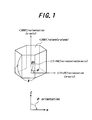
- Fig. 1 is a crystal structure of sapphire single crystal.
- the crystal orientation of the main surface of the sapphire single crystal base material to constitute the epitaxial substrate is inclined from the ⁇ 0001> orientation, that is, the c-axis orientation by a range within 0.02-0.3 degrees, preferably 0.05-0.25 degrees, more preferably 0.07-0.2 degrees.
- the dislocation density of an Al-including nitride underfilm to be formed on the main surface of the base material can be reduced, and thus, the dislocation density of the epitaxial substrate can be reduced entirely, concretely to a range of 5 ⁇ 10 10 /cm 2 or below, particularly 10 9 /cm 2 or below, more particularly 10 8 /cm 2 or below.
- the full width at half maximum (FWHM) at (10-12) reflection in X-ray rocking curve of the Al-including nitride underfilm can be improved to a range of 2000 seconds or below, particularly 1700 seconds or below, more particularly 1500 seconds or below.
- the surface roughness (Ra) of the Al-including nitride underfilm can be reduced to a range of 3.5 ⁇ or below, particularly 2.5 ⁇ or below, particularly 2.0 ⁇ or below per 5 ⁇ m area. Therefore, the crystal quality of the Al-including nitride underfilm can be enhanced.
- the inclination angle that is, the off-angle of the c-faced sapphire single crystal base material is set within the above-mentioned preferable range, the function/effect of the surface nitride layer can be exhibited most effectively, and thus, the dislocation density of the epitaxial substrate can be reduced most effectively.
- the off-angle of the c-faced sapphire single crystal base material is set beyond 0.3 degrees, the surface roughness of the base material is deteriorated due to generation of pits, and thus, the crystal qualities of the Al-including nitride underfilm and a given Al-including nitride film to be formed on the underfilm are also deteriorated, due to the surface roughness of the base material.
- the inclination direction of the c-faced sapphire single crystal base material is set to the ⁇ 1-100> orientation, that is, the m-axis orientation.
- the function/operation of the surface nitride layer can be exhibited effectively, and the dislocation density of the epitaxial substrate can be reduced sufficiently.
- the sapphire single crystal base material has a hexagonal crystal structure as illustrated in Fig. 1, and the c-axis, the m-axis and the a-axis satisfy the physical relationship as illustrated in Figs. 1. Therefore, the c-axis of the sapphire single crystal base material is preferably inclined to the m-axis by ⁇ angle on Fig. 1.
- the surface nitride layer is formed at the off-angled main surface of the c-faced sapphire single crystal base material.
- the surface nitride layer is formed thick so that the nitrogen content at a depth of 1nm from the main surface of the surface nitride layer is preferably set to a range of 2 atomic percentages, more preferably within 5- 50 atomic percentages.
- the depth and the nitrogen content are measured from the compositional analysis of the c-faced sapphire single crystal base material in the thickness direction by means of ESCA when the c-faced sapphire single crystal base material is etched in the thickness direction with Ar ions.
- ESCA measuring conditions will be shown as follows.
- a X-ray having an energy of 1253.6eV from a Mg target was employed as a X-ray source.
- the measuring region was set to 1.1mm ⁇ , and the detection angle was set to 45 degrees.
- the pass energy was set to 35.75eV.
- the existence of nitrogen was determined on Nls spectrum.
- the measuring degree of vacuum was set to 3 ⁇ 10 -9 Torr.
- the etching process was carried out by utilizing Ar + ions having an accelerating voltage of 3.0kV.
- the raster region was set to 3mm ⁇ 3mm.
- the etching rate was set to 40 ⁇ /min for SiO 2 , and the etching rate of Al 2 O 3 was one-third of that of SiO 2 . Therefore, the etching rate of the surface nitride layer was conveniently calculated from the Al 2 O 3 etching rate. That is, the nitrogen content at the depth of 1nm of the base material is defined by calculating back the etching period for a 1nm depth of the surface nitride layer from the etching rate of Al 2 O 3 for the etching rate of the surface nitride layer.
- the surface nitride layer can be formed by setting the c-faced sapphire single crystal base material in a nitrogen-including atmosphere, for example in an ammonia atmosphere and heating the base material for a predetermined period. In this case, the nitrogen concentration, the nitriding temperature and the nitriding period are appropriately adjusted.
- the Al-including III nitride underfilm is formed on the off-angled main surface of the c-faced sapphire single crystal base material via the surface nitride layer. If a III nitride film particularly including Al element is formed on the nitride underfilm, the crystallinity and the dislocation density of the III nitride film can be enhanced. In this point of view, it is desired to develop the crystallinity of the nitride underfilm. Concretely, it is desired that the FWHM at (0002) reflection of the nitride underfilm is improved to a range of 100 seconds or below.
- the high crystal quality III nitride film underfilm can be made by means of a MOCVD method where the c-faced sapphire single crystal base material itself is heated at a temperature range of 1100°C or over, preferably 1250°C or below.
- the III nitride underfilm serves as sort of a buffer layer because it is located between the sapphire single crystal base material and the III nitride film to be formed.
- a low crystallinity AlN or GaN buffer layer is formed by heating a sapphire single crystal base material to a temperature range of 500-600°C by means of a MOCVD method so as to mitigate the difference in lattice constant between the Ga-based nitride films and the sapphire single crystal base material.
- the crystal quality of the III nitride film can be improved due to the high crystal quality of the III nitride underfilm as mentioned above.
- the crystal quality developing tendency of the III nitride film becomes conspicuous as the Al content of the III nitride underfilm increases.
- the Al content of the III nitride underfilm is preferably set to a range of 50 atomic percentages or over for all of the III elements, and particularly, the III nitride underfilm is preferably made of AlN (Al content of 100 atomic percentages).
- the III nitride underfilm may contain B, Si, Ge, Zn, Be, Mg or the like. Moreover, the underfilm may contain inevitable minute element and minute impurities depending on the film-forming condition, the supply source and the reactor material, in addition to the above-mentioned intentional elements.
- the thickness of the III nitride underfilm is preferably set to a range of 0.5 ⁇ m or over, particularly within 0.7-3 ⁇ m. Since the sapphire single crystal base material satisfies the above-mentioned requirements of the present invention, no cracks are created and no exfoliation occurs even though the III nitride underfilm is formed thick as mentioned above.
- a photonic device such as a semiconductor light-emitting element or a semiconductor light-detecting element, an electronic device or a field emitter can be fabricated.
- the one or plural III nitride films are formed on the epitaxial substrate of the present invention, so the crystal quality of low dislocation density and high crystallinity thereof can be realized, so the efficiency of the photonic device or the electron device can be also improved.
- the one or plural III nitride films may be formed by using the same MOCVD apparatus as the one whereby the epitaxial substrate is fabricated. Also, they may be formed by using a different MOCVD apparatus.
- a c-faced sapphire single crystal base material having a main surface off angled by 0.15 degrees for the m-axis was employed, and then, set and attracted on a susceptor installed in a quartz reactor. Thereafter, the base material was heated to 1200°C with the heater built in the susceptor.
- an ammonia (NH 3 ) gas was supplied with a carrier gas onto the base material to nitride the main surface of the base material. It was turned out from ESCA analysis that a nitride layer was formed at the main surface of the base material by the surface nitriding treatment and the nitrogen content at a depth of 1nm from the main surface was seven atomic percentages.
- TMA trimethyl aluminum
- the FWHM at (0002) reflection was about 70 seconds and the FWHM at (10-12) reflection was about 1000 seconds. Therefore, it was turned out that the AlN underfilm has good crystallinity.
- the surface roughness Ra of the AlN underfilm was 1.5 ⁇ within 5 ⁇ m area, and it was also turned out that the AlN underfilm has good flatness.
- the dislocation density of the AlN underfilm was 5 ⁇ 10 9 /cm 2 .
- TMG trimethyl gallium
- a c-faced sapphire single crystal base material having a main surface off angled by 0.07 degrees for the m-axis was employed. Then, a surface nitriding treatment was carried out in the same manner as in Example 1, and an AlN underfilm was formed in the same manner as in Example 1.
- the crystallinity of the AlN underfilm was measured by means of X-ray rocking curve analysis ( ⁇ -scan)
- the FWHM at (0002) reflection was about 70 seconds and the FWHM at (10-12) reflection was about 1300 seconds.
- the surface roughness Ra of the AlN underfilm was 1.5 ⁇ within 5 ⁇ m area.
- the dislocation density of the AlN underfilm was 7 ⁇ 10 9 /cm 2 .
- a c-faced sapphire single crystal base material having a main surface off angled by 0.15 degrees for the a-axis was employed. Then, a surface nitriding treatment was carried out in the same manner as in Example 1, and an AlN underfilm was formed in the same manner as in Example 1.
- the crystallinity of the AlN underfilm was measured by means of X-ray rocking curve analysis ( ⁇ -scan)
- the FWHM at (0002) reflection was about 70 seconds and the FWHM at (10-12) reflection was about 1300 seconds.
- the surface roughness Ra of the AlN underfilm was 1.5 ⁇ within 5 ⁇ m area.
- the dislocation density of the AlN underfilm was 7 ⁇ 10 9 /cm 2 .
- a c-faced sapphire single crystal base material having a main surface off angled by 0.02 degrees for the m-axis was employed. Then, a surface nitriding treatment was carried out in the same manner as in Example 1, and an AlN underfilm was formed in the same manner as in Example 1.
- the crystallinity of the AlN underfilm was measured by means of X-ray rocking curve analysis ( ⁇ -scan)
- the FWHM at (0002) reflection was about 70 seconds and the FWHM at (10-12) reflection was about 1800 seconds.
- the surface roughness Ra of the AlN underfilm was 1.5 ⁇ within 5 ⁇ m area.
- the dislocation density of the AlN underfilm was 3 ⁇ 10 10 /cm 2 .
- a c-faced sapphire single crystal base material having a main surface off angled by 0.3 degrees for the m-axis was employed. Then, a surface nitriding treatment was carried out in the same manner as in Example 1, and an AlN underfilm was formed in the same manner as in Example 1.
- the crystallinity of the AlN underfilm was measured by means of X-ray rocking curve analysis ( ⁇ -scan)
- the FWHM at (0002) reflection was about 70 seconds and the FWHM at (10-12) reflection was about 1500 seconds.
- the surface roughness Ra of the AlN underfilm was 3.0 ⁇ within 5 ⁇ m area.
- the dislocation density of the AlN underfilm was 2 ⁇ 10 10 /cm 2 .
- a c-faced sapphire single crystal base material having a main surface off angled by 0.15 degrees for the m-axis was employed. Then, an AlN underfilm was formed directly on the base material in the same manner as in Example 1 without a surface nitriding treatment.
- the crystallinity of the AlN underfilm was measured by means of X-ray rocking curve analysis ( ⁇ -scan), the FWHM at (0002) reflection was about 250 seconds and the FWHM at (10-12) reflection was about 1800 seconds.
- the surface roughness Ra of the AlN underfilm was 1.5 ⁇ within 5 ⁇ m area.
- the dislocation density of the AlN underfilm was 3 ⁇ 10 10 /cm 2 .
- a c-faced sapphire single crystal base material having a main surface off angled by 0.4 degrees for the m-axis was employed. Then, a surface nitriding treatment was carried out in the same manner as in Example 1, and an AlN underfilm was formed in the same manner as in Example 1.
- the crystallinity of the AlN underfilm was measured by means of X-ray rocking curve analysis ( ⁇ -scan)
- the FWHM at (0002) reflection was about 70 seconds
- the FWHM at (10-12) reflection was about 1500 seconds.
- the surface roughness Ra of the AlN underfilm was 4.0 ⁇ within 5 ⁇ m area, and many pits and step bunchings were observed in the AlN underfilm.
- the dislocation density of the AlN underfilm was 7 ⁇ 10 10 /cm 2 .
- a c-faced sapphire single crystal base material having a main surface off angled by 0.01 degrees or below for the m-axis was employed. Then, a surface nitriding treatment was carried out in the same manner as in Example 1, and an AlN underfilm was formed in the same manner as in Example 1.
- the crystallinity of the AlN underfilm was measured by means of X-ray rocking curve analysis ( ⁇ -scan)
- the FWHM at (0002) reflection was about 70 seconds
- the FWHM at (10-12) reflection was about 2500 seconds.
- the surface roughness Ra of the AlN underfilm was 1.5 ⁇ within 5 ⁇ m area, and pits were observed in the AlN underfilm.
- the dislocation density of the AlN underfilm was 5 ⁇ 10 10 /cm 2 .
- a buffer layer or a multi-layered structure such as a distorted superstructure may be provided between the epitaxial substrate and an Al-including nitride film to be formed.
- the crystallinity of the Al-including nitride film can be improved.
- a sapphire single crystal base material and a new epitaxial substrate including the sapphire single crystal base material, whereby a nitride film having high crystal quality can be formed can be provided.
Landscapes
- Chemical & Material Sciences (AREA)
- Engineering & Computer Science (AREA)
- Crystallography & Structural Chemistry (AREA)
- Materials Engineering (AREA)
- Metallurgy (AREA)
- Organic Chemistry (AREA)
- Inorganic Chemistry (AREA)
- Chemical Kinetics & Catalysis (AREA)
- General Chemical & Material Sciences (AREA)
- Led Devices (AREA)
- Crystals, And After-Treatments Of Crystals (AREA)
Abstract
Description
- This invention relates to a III nitride epitaxial substrate, an epitaxial substrate for III nitride element and a III nitride element, particularly a III nitride epitaxial substrate suitable for a semiconductor nitride element such as a photonic device, an electronic device or a field emitter, a III nitride element such as a photonic device made of the III nitride film epitaxial film, and an epitaxial substrate for the III nitride element.
- III nitride films are used as semiconductor films for light-emitting diodes and electronic devices, and recently get attention as semiconductor films for high speed IC chips. Particularly, Al-including III nitride films get attention as field emitter materials.
- Such a III nitride film is formed on an epitaxial substrate, for example, which has an underfilm epitaxially grown on a given base material. A sapphire single crystal is employed as the base material because it is not expensive and easily available.
- The underfilm is preferably made of an Al-including III nitride film in order to facilitate the epitaxial growth of the III nitride film to be formed. Moreover, since such an Al-including III nitride film has a larger bandgap, if it is formed between a base material and a given III nitride film, it can enhance the efficiency of the resultant semiconductor element.
- The epitaxial substrate is set on a susceptor installed in a given reactor, and heated to a predetermined temperature with a heater built in or out of the susceptor. Then, a III metallic supply source, a nitrogen supply source and another element supply source if desired are introduced into the reactor with a carrier gas, and supplied onto the epitaxial substrate to fabricate the III nitride film by an MOCVD method.
- In the case of the use of the epitaxial substrate, a large amount of misfit dislocations may be created due to the difference in lattice constant between the sapphire single crystal base material and the Al-including III nitride underfilm, and propagated as penetrating dislocations through the III nitride underfilm to reach the surface of the epitaxial substrate. If the III nitride film is made on the epitaxial substrate, a large amount of dislocations may be created in the III nitride film, originated from the propagated misfit dislocations.
- The above-mentioned similar phenomenon can be observed when a Ga-including or another III nitride underfilm as well as the Al-including III nitride underfilm is formed on the sapphire single crystal base material.
- In other words, in the case of the use of the sapphire single crystal base material, only a low crystal quality III nitride film including a relatively large amount of dislocations can be formed, so that if a semiconductor light-emitting element is fabricated by utilizing the low crystal quality III nitride film, the luminous efficiency of the semiconductor element is deteriorated. And if a electronic device element such as HEMT, HBT is fabricated by utilizing the low crystal quality III nitride film, electrical mobility goes down or leak electric current increases. As a result, the semiconductor element can not exhibit the inherent performances as designed.
- It is an object of the present invention to provide a new epitaxial substrate having a sapphire single crystal base material and an Al-including III nitride underfilm, whereby a high crystalinity nitride film, particularly an Al-including nitride film, including much less dislocations, can be formed.
- In order to achieve the above object, this invention relates to a III nitride epitaxial substrate comprising;
- a sapphire single crystal base material of which a crystal orientation of a main surface is inclined from the <0001> orientation by a range within 0.02-0.3 degrees and which includes a surface nitride layer at the main surface, and
- a III nitride underfilm which is formed on the main surface of the sapphire single crystal base material via the surface nitride layer and includes at least Al element, and of which a full width at half maximum at (10-12) reflection in X-ray rocking curve is 2000 seconds or below and of which a surface roughness Ra within 5 µm area is 3.5Å.
-
- The inventors had intensely studied to develop an epitaxial substrate on which the high crystallinity nitride film, particularly the Al-including nitride film, including low dislocation density, can be formed. Then, the inventors had made vast researches and developments about sapphire single crystal base materials to constitute epitaxial substrates. As a result, the inventors found out that the crystallinity and the physical properties of the main surface of the base material on which the nitride film is formed affect eventfully on the creation of dislocation between the sapphire single crystal base material and the Al-including III nitride underfilm, so conceived the present invention.
- Since the epitaxial substrate of the present invention can exhibit good crystal quality of low dislocation density, the dislocation density of a III nitride film particularly including Al element to be formed on the epitaxial substrate can be reduced, and thus, the crystal quality can be enhanced.
- Such a technique is disclosed in Japanese Patent Application Laid-open No. 2000-82676 as that by inclining the crystal orientation of the main surface of a sapphire single crystal base material from the <0001> orientation by 0.05-0.20 degrees, the dislocation density of a III nitride film formed on the main surface of the base material is reduced. In this case, however, the base material is composed only of a sapphire single crystal, and is employed exclusively for fabricating a semiconductor layer group made of Ga-based nitride films.
- However, if a semiconductor layer group particularly made of Al-based nitride films is fabricated on a sapphire single crystal base material as described in the above conventional technique, the dislocation density of the semiconductor layer group can not be reduced. In order to reduce the dislocation densities of the Al-based nitride films, it is required that the main surface of a sapphire single crystal base material is inclined and a surface nitride layer is formed at the main surface of the base material, according to the present invention. Also, it is required that an Al-including nitride film is formed on the main surface of the base material.
- If the surface nitride layer is formed according to the present invention, the inclination angle of the main surface of the base material can be increased to a range within 0.05-0.25 degrees, particularly a range within 0.05-0.3 degrees, from a conventional range within 0.05-0.20 degrees. As a result, the selectivity of the sapphire single crystal base material can be increased, and thus, the degree of freedom in design of the resultant semiconductor element can be also increased.
- For better understanding of the present invention, reference is made to the attached drawings, wherein
Fig. 1 is a crystal structure of sapphire single crystal. - This invention will be described in detail, hereinafter.
- It is required in the present invention that the crystal orientation of the main surface of the sapphire single crystal base material to constitute the epitaxial substrate is inclined from the <0001> orientation, that is, the c-axis orientation by a range within 0.02-0.3 degrees, preferably 0.05-0.25 degrees, more preferably 0.07-0.2 degrees. In other words, it is required in the present invention to employ an off-angled sapphire single crystal base material of which the c-face is inclined by the above-mentioned range.
- Then, if the surface nitride layer is formed at the main surface of the base material according to the present invention, the dislocation density of an Al-including nitride underfilm to be formed on the main surface of the base material can be reduced, and thus, the dislocation density of the epitaxial substrate can be reduced entirely, concretely to a range of 5×10¹⁰/cm2 or below, particularly 109/cm2 or below, more particularly 108/cm2 or below.
- In this case, the full width at half maximum (FWHM) at (10-12) reflection in X-ray rocking curve of the Al-including nitride underfilm can be improved to a range of 2000 seconds or below, particularly 1700 seconds or below, more particularly 1500 seconds or below. In addition, the surface roughness (Ra) of the Al-including nitride underfilm can be reduced to a range of 3.5Å or below, particularly 2.5Å or below, particularly 2.0Å or below per 5 µm area. Therefore, the crystal quality of the Al-including nitride underfilm can be enhanced.
- If the inclination angle, that is, the off-angle of the c-faced sapphire single crystal base material is set within the above-mentioned preferable range, the function/effect of the surface nitride layer can be exhibited most effectively, and thus, the dislocation density of the epitaxial substrate can be reduced most effectively.
- If the off-angle of the c-faced sapphire single crystal base material is set beyond 0.3 degrees, the surface roughness of the base material is deteriorated due to generation of pits, and thus, the crystal qualities of the Al-including nitride underfilm and a given Al-including nitride film to be formed on the underfilm are also deteriorated, due to the surface roughness of the base material.
- It is desired that the inclination direction of the c-faced sapphire single crystal base material is set to the <1-100> orientation, that is, the m-axis orientation. In this case, the function/operation of the surface nitride layer can be exhibited effectively, and the dislocation density of the epitaxial substrate can be reduced sufficiently.
- The sapphire single crystal base material has a hexagonal crystal structure as illustrated in Fig. 1, and the c-axis, the m-axis and the a-axis satisfy the physical relationship as illustrated in Figs. 1. Therefore, the c-axis of the sapphire single crystal base material is preferably inclined to the m-axis by angle on Fig. 1.
- In the present invention, it is required that the surface nitride layer is formed at the off-angled main surface of the c-faced sapphire single crystal base material. The surface nitride layer is formed thick so that the nitrogen content at a depth of 1nm from the main surface of the surface nitride layer is preferably set to a range of 2 atomic percentages, more preferably within 5- 50 atomic percentages.
- Herein, the depth and the nitrogen content are measured from the compositional analysis of the c-faced sapphire single crystal base material in the thickness direction by means of ESCA when the c-faced sapphire single crystal base material is etched in the thickness direction with Ar ions.
- Detailed ESCA measuring conditions will be shown as follows. A X-ray having an energy of 1253.6eV from a Mg target was employed as a X-ray source. The measuring region was set to 1.1mm, and the detection angle was set to 45 degrees. The pass energy was set to 35.75eV. The existence of nitrogen was determined on Nls spectrum. The measuring degree of vacuum was set to 3×10⁻⁹Torr. The etching process was carried out by utilizing Ar+ ions having an accelerating voltage of 3.0kV. The raster region was set to 3mm×3mm.
- In this case, the etching rate was set to 40Å/min for SiO2, and the etching rate of Al2O3 was one-third of that of SiO2. Therefore, the etching rate of the surface nitride layer was conveniently calculated from the Al2O3 etching rate. That is, the nitrogen content at the depth of 1nm of the base material is defined by calculating back the etching period for a 1nm depth of the surface nitride layer from the etching rate of Al2O3 for the etching rate of the surface nitride layer.
- The surface nitride layer can be formed by setting the c-faced sapphire single crystal base material in a nitrogen-including atmosphere, for example in an ammonia atmosphere and heating the base material for a predetermined period. In this case, the nitrogen concentration, the nitriding temperature and the nitriding period are appropriately adjusted.
- In the present invention, it is also required that the Al-including III nitride underfilm is formed on the off-angled main surface of the c-faced sapphire single crystal base material via the surface nitride layer. If a III nitride film particularly including Al element is formed on the nitride underfilm, the crystallinity and the dislocation density of the III nitride film can be enhanced. In this point of view, it is desired to develop the crystallinity of the nitride underfilm. Concretely, it is desired that the FWHM at (0002) reflection of the nitride underfilm is improved to a range of 100 seconds or below.
- The high crystal quality III nitride film underfilm can be made by means of a MOCVD method where the c-faced sapphire single crystal base material itself is heated at a temperature range of 1100°C or over, preferably 1250°C or below.
- The III nitride underfilm serves as sort of a buffer layer because it is located between the sapphire single crystal base material and the III nitride film to be formed. Conventionally, in the case of the fabrication of Ga-based nitride films, a low crystallinity AlN or GaN buffer layer is formed by heating a sapphire single crystal base material to a temperature range of 500-600°C by means of a MOCVD method so as to mitigate the difference in lattice constant between the Ga-based nitride films and the sapphire single crystal base material.
- In the present invention, however, even though the high crystallinity III nitride underfilm is formed between the sapphire single crystal base material and III nitride films to be formed, misfit dislocations are not almost created due to the difference in lattice constant therebetween because the sapphire single crystal base material satisfies the above-mentioned requirements. Therefore, the crystal quality of the III nitride film can be improved due to the high crystal quality of the III nitride underfilm as mentioned above.
- The crystal quality developing tendency of the III nitride film becomes conspicuous as the Al content of the III nitride underfilm increases. In this point of view, the Al content of the III nitride underfilm is preferably set to a range of 50 atomic percentages or over for all of the III elements, and particularly, the III nitride underfilm is preferably made of AlN (Al content of 100 atomic percentages).
- The III nitride underfilm may contain B, Si, Ge, Zn, Be, Mg or the like. Moreover, the underfilm may contain inevitable minute element and minute impurities depending on the film-forming condition, the supply source and the reactor material, in addition to the above-mentioned intentional elements.
- The thickness of the III nitride underfilm is preferably set to a range of 0.5 µm or over, particularly within 0.7-3 µm. Since the sapphire single crystal base material satisfies the above-mentioned requirements of the present invention, no cracks are created and no exfoliation occurs even though the III nitride underfilm is formed thick as mentioned above.
- If one or plural III nitride films are formed on the epitaxial substrate fabricated so as to satisfy the above-mentioned requirements of the present invention, a photonic device such as a semiconductor light-emitting element or a semiconductor light-detecting element, an electronic device or a field emitter can be fabricated.
- Since the one or plural III nitride films are formed on the epitaxial substrate of the present invention, the crystal quality of low dislocation density and high crystallinity thereof can be realized, so the efficiency of the photonic device or the electron device can be also improved.
- Herein, the one or plural III nitride films may be formed by using the same MOCVD apparatus as the one whereby the epitaxial substrate is fabricated.
Also, they may be formed by using a different MOCVD apparatus. - This invention will be concretely described hereinafter.
- A c-faced sapphire single crystal base material having a main surface off angled by 0.15 degrees for the m-axis was employed, and then, set and attracted on a susceptor installed in a quartz reactor. Thereafter, the base material was heated to 1200°C with the heater built in the susceptor.
- Then, an ammonia (NH3) gas was supplied with a carrier gas onto the base material to nitride the main surface of the base material. It was turned out from ESCA analysis that a nitride layer was formed at the main surface of the base material by the surface nitriding treatment and the nitrogen content at a depth of 1nm from the main surface was seven atomic percentages.
- Then, a trimethyl aluminum (TMA) as a Al supply source and an NH3 gas as a nitrogen supply source were employed, and introduced with a hydrogen carrier gas into the reactor at a flow rate ratio of NH3/TMA=500 and supplied onto the base material to form an AlN underfilm in a thickness of 1 µm on the base material. Herein, the flow rates of NH3 and TMA were appropriately controlled on the film-forming rate at the above flow rate ratio.
- When the crystallinity of the AlN underfilm was measured by means of X-ray rocking curve analysis (ω-scan), the FWHM at (0002) reflection was about 70 seconds and the FWHM at (10-12) reflection was about 1000 seconds. Therefore, it was turned out that the AlN underfilm has good crystallinity.
The surface roughness Ra of the AlN underfilm was 1.5Å within 5 µm area, and it was also turned out that the AlN underfilm has good flatness. The dislocation density of the AlN underfilm was 5×10⁹/cm2. - Then, a trimethyl gallium (TMG) as a Ga supply source was also introduced into the reactor at a flow rate ratio of NH3/(TMA+TMG)=2000 with hydrogen carrier gas and supplied onto the AlN underfilm to form an Al0.1Ga0.9N film in a thickness of 3 µm. When the dislocation density of the Al0.1Ga0.9N film was measured by means of TEM observation, it was turned out to be 1×10⁸/cm2.
- A c-faced sapphire single crystal base material having a main surface off angled by 0.07 degrees for the m-axis was employed. Then, a surface nitriding treatment was carried out in the same manner as in Example 1, and an AlN underfilm was formed in the same manner as in Example 1. When the crystallinity of the AlN underfilm was measured by means of X-ray rocking curve analysis (ω-scan), the FWHM at (0002) reflection was about 70 seconds and the FWHM at (10-12) reflection was about 1300 seconds. The surface roughness Ra of the AlN underfilm was 1.5Å within 5 µm area. The dislocation density of the AlN underfilm was 7×10⁹/cm2.
- Then, an Al0.1Ga0.9N film was formed on the AlN underfilm in the same manner as in Example 1. When the dislocation density of the Al0.1Ga0.9N film was measured by means of TEM observation, it was turned out to be 2×10⁸/cm2.
- A c-faced sapphire single crystal base material having a main surface off angled by 0.15 degrees for the a-axis was employed. Then, a surface nitriding treatment was carried out in the same manner as in Example 1, and an AlN underfilm was formed in the same manner as in Example 1. When the crystallinity of the AlN underfilm was measured by means of X-ray rocking curve analysis (ω-scan), the FWHM at (0002) reflection was about 70 seconds and the FWHM at (10-12) reflection was about 1300 seconds. The surface roughness Ra of the AlN underfilm was 1.5Å within 5 µm area. The dislocation density of the AlN underfilm was 7×10⁹/cm2.
- Then, an Al0.1Ga0.9N film was formed on the AlN underfilm in the same manner as in Example 1. When the dislocation density of the Al0.1Ga0.9N film was measured by means of TEM observation, it was turned out to be 2×10⁸/cm2.
- A c-faced sapphire single crystal base material having a main surface off angled by 0.02 degrees for the m-axis was employed. Then, a surface nitriding treatment was carried out in the same manner as in Example 1, and an AlN underfilm was formed in the same manner as in Example 1. When the crystallinity of the AlN underfilm was measured by means of X-ray rocking curve analysis (ω-scan), the FWHM at (0002) reflection was about 70 seconds and the FWHM at (10-12) reflection was about 1800 seconds. The surface roughness Ra of the AlN underfilm was 1.5Å within 5 µm area. The dislocation density of the AlN underfilm was 3×10¹⁰/cm2.
- Then, an Al0.1Ga0.9N film was formed on the AlN underfilm in the same manner as in Example 1. When the dislocation density of the Al0.1Ga0.9N film was measured by means of TEM observation, it was turned out to be 5×10⁸/cm2.
- A c-faced sapphire single crystal base material having a main surface off angled by 0.3 degrees for the m-axis was employed. Then, a surface nitriding treatment was carried out in the same manner as in Example 1, and an AlN underfilm was formed in the same manner as in Example 1. When the crystallinity of the AlN underfilm was measured by means of X-ray rocking curve analysis (ω-scan), the FWHM at (0002) reflection was about 70 seconds and the FWHM at (10-12) reflection was about 1500 seconds. The surface roughness Ra of the AlN underfilm was 3.0Å within 5 µm area. The dislocation density of the AlN underfilm was 2×10¹⁰/cm2.
- Then, an Al0.1Ga0.9N film was formed on the AlN underfilm in the same manner as in Example 1. When the dislocation density of the Al0.1Ga0.9N film was measured by means of TEM observation, it was turned out to be 5×10⁸/cm2.
- A c-faced sapphire single crystal base material having a main surface off angled by 0.15 degrees for the m-axis was employed. Then, an AlN underfilm was formed directly on the base material in the same manner as in Example 1 without a surface nitriding treatment. When the crystallinity of the AlN underfilm was measured by means of X-ray rocking curve analysis (ω-scan), the FWHM at (0002) reflection was about 250 seconds and the FWHM at (10-12) reflection was about 1800 seconds. The surface roughness Ra of the AlN underfilm was 1.5Å within 5 µm area. The dislocation density of the AlN underfilm was 3×10¹⁰/cm2.
- Then, an Al0.1Ga0.9N film was formed on the AlN underfilm in the same manner as in Example 1. When the dislocation density of the Al0.1Ga0.9N film was measured by means of TEM observation, it was turned out to be 8×10⁹/cm2.
- A c-faced sapphire single crystal base material having a main surface off angled by 0.4 degrees for the m-axis was employed. Then, a surface nitriding treatment was carried out in the same manner as in Example 1, and an AlN underfilm was formed in the same manner as in Example 1. When the crystallinity of the AlN underfilm was measured by means of X-ray rocking curve analysis (ω-scan), the FWHM at (0002) reflection was about 70 seconds and the FWHM at (10-12) reflection was about 1500 seconds. The surface roughness Ra of the AlN underfilm was 4.0Å within 5 µm area, and many pits and step bunchings were observed in the AlN underfilm. The dislocation density of the AlN underfilm was 7×10¹⁰/cm2.
- Then, an Al0.1Ga0.9N film was formed on the AlN underfilm in the same manner as in Example 1. When the dislocation density of the Al0.1Ga0.9N film was measured by means of TEM observation, it was turned out to be 8×10⁹/cm2.
- A c-faced sapphire single crystal base material having a main surface off angled by 0.01 degrees or below for the m-axis was employed. Then, a surface nitriding treatment was carried out in the same manner as in Example 1, and an AlN underfilm was formed in the same manner as in Example 1. When the crystallinity of the AlN underfilm was measured by means of X-ray rocking curve analysis (ω-scan), the FWHM at (0002) reflection was about 70 seconds and the FWHM at (10-12) reflection was about 2500 seconds. The surface roughness Ra of the AlN underfilm was 1.5Å within 5 µm area, and pits were observed in the AlN underfilm. The dislocation density of the AlN underfilm was 5×10¹⁰/cm2.
- Then, an Al0.1Ga0.9N film was formed on the AlN underfilm in the same manner as in Example 1. When the dislocation density of the Al0.1Ga0.9N film was measured by means of TEM observation, it was turned out to be 1×10¹⁰/cm2.
- As is apparent from Examples and Comparative Examples, the crystal quality of crystallinity and dislocation density and the surface flatness of the AlN underfilm to constitute an epitaxial substrate according to the present invention are improved. Therefore, the crystal quality of dislocation density of the Al0.1Ga0.9N film is also realized.
- As is apparent from Examples 1-3, if the inclination angle of the c-faced sapphire single crystal base material, that is, the off-angle of the main surface of the base material is set within 0.07-0.2 degrees, the crystallinity and the dislocation density of the AlN underfilm is much improved, and thus, the dislocation density of the Al0.1Ga0.9N film is much reduced.
- Similarly, as is apparent from Examples 1 and 3, if the c-faced sapphire single crystal base material is inclined for the m-axis, not a-axis, the crystallinity and the dislocation density of the AlN underfilm is much improved, and thus, the dislocation density of the Al0.1Ga0.9N film is much reduced.
- Although the present invention was described in detail with reference to the above examples, this invention is not limited to the above disclosure and every kind of variation and modification may be made without departing from the scope of the present invention. For example, a buffer layer or a multi-layered structure such as a distorted superstructure may be provided between the epitaxial substrate and an Al-including nitride film to be formed. In this case, the crystallinity of the Al-including nitride film can be improved.
- As mentioned above, a sapphire single crystal base material and a new epitaxial substrate including the sapphire single crystal base material, whereby a nitride film having high crystal quality can be formed, can be provided.
Claims (13)
- A III nitride epitaxial substrate comprising;
a sapphire single crystal base material of which a crystal orientation of a main surface is inclined from the <0001> orientation by a range within 0.02-0.3 degrees and which includes a surface nitride layer at said main surface, and
an III nitride underfilm which is formed on said main surface of said sapphire single crystal base material via said surface nitride layer and includes at least Al element, and of which a full width at half maximum at (10-12) reflection in X-ray rocking curve is 2000 seconds or below and of which a surface roughness Ra within 5 µm area is 3.5Å. - The III nitride epitaxial substrate as defined in claim 1, wherein said crystal orientation of said main surface of said sapphire single crystal base material is inclined from <0001> orientation by a range within 0.05-0.25 degrees.
- The III nitride epitaxial substrate as defined in claim 2, wherein said crystal orientation of said main surface of said sapphire single crystal base material is inclined from <0001> orientation by a range within 0.07-0.20 degrees.
- The III nitride epitaxial substrate as defined in any one of claims 1-3, wherein said crystal orientation of said main surface of said sapphire single crystal base material is inclined from <0001> orientation for the <1-100) orientation.
- The III nitride epitaxial substrate as defined in any one of claims 1-4, wherein said full width at half maximum at (10-12) reflection in X-ray rocking curve of said III nitride underfilm is 1700 seconds or below and said surface roughness Ra within 5 µm area of said III nitride underfilm is 2.5Å.
- The III nitride epitaxial substrate as defined in claim 5, wherein said full width at half maximum at (10-12) reflection in X-ray rocking curve of said III nitride underfilm is 1500 seconds or below and said surface roughness Ra within 5 µm area of said III nitride underfilm is 2.0Å.
- The III nitride epitaxial substrate as defined in any one of claims 1-6, wherein the nitrogen content of said surface nitride layer is set to a range of 2 atomic percentages or over at a depth of 1nm from said main surface of said sapphire single crystal base material.
- The III nitride epitaxial substrate as defined in claim 7, wherein the nitrogen content of said surface nitride layer is set to a range within 2-50 atomic percentages at a depth of 1nm from said main surface of said sapphire single crystal base material.
- The III nitride epitaxial substrate as defined in any one of claims 1-8, wherein a full width at half maximum at (0002) reflection in X-ray rocking curve of said III nitride underfilm is 100 seconds or below.
- The III nitride epitaxial substrate as defined in any one of claims 1-9, wherein the Al content of said III nitride under film is set to a range of 50 atomic percentages or over for all of the III elements.
- The III nitride epitaxial substrate as defined in claim 10, wherein said III nitride underfilm is made of AlN.
- An epitaxial substrate for III nitride element comprising a III nitride epitaxial substrate as defined in any one of claims 1-11.
- A III nitride element comprising a III nitride epitaxial substrate as defined in any one of claims 1-11.
Applications Claiming Priority (6)
| Application Number | Priority Date | Filing Date | Title |
|---|---|---|---|
| JP2001300288 | 2001-09-28 | ||
| JP2001300288 | 2001-09-28 | ||
| JP2002249187 | 2002-08-28 | ||
| JP2002249187 | 2002-08-28 | ||
| JP2002268349 | 2002-09-13 | ||
| JP2002268349A JP3768943B2 (en) | 2001-09-28 | 2002-09-13 | Group III nitride epitaxial substrate, group III nitride device epitaxial substrate, and group III nitride device |
Publications (3)
| Publication Number | Publication Date |
|---|---|
| EP1298709A2 true EP1298709A2 (en) | 2003-04-02 |
| EP1298709A3 EP1298709A3 (en) | 2009-08-26 |
| EP1298709B1 EP1298709B1 (en) | 2017-03-22 |
Family
ID=27347608
Family Applications (1)
| Application Number | Title | Priority Date | Filing Date |
|---|---|---|---|
| EP02021450.8A Expired - Lifetime EP1298709B1 (en) | 2001-09-28 | 2002-09-25 | Method for producing a iii nitride element comprising a iii nitride epitaxial substrate |
Country Status (3)
| Country | Link |
|---|---|
| US (1) | US6844611B2 (en) |
| EP (1) | EP1298709B1 (en) |
| JP (1) | JP3768943B2 (en) |
Cited By (4)
| Publication number | Priority date | Publication date | Assignee | Title |
|---|---|---|---|---|
| US7045223B2 (en) | 2003-09-23 | 2006-05-16 | Saint-Gobain Ceramics & Plastics, Inc. | Spinel articles and methods for forming same |
| US7326477B2 (en) | 2003-09-23 | 2008-02-05 | Saint-Gobain Ceramics & Plastics, Inc. | Spinel boules, wafers, and methods for fabricating same |
| US7919815B1 (en) | 2005-02-24 | 2011-04-05 | Saint-Gobain Ceramics & Plastics, Inc. | Spinel wafers and methods of preparation |
| CN106067500A (en) * | 2010-08-06 | 2016-11-02 | 日亚化学工业株式会社 | Sapphire substrate and semiconductor light emitting element |
Families Citing this family (16)
| Publication number | Priority date | Publication date | Assignee | Title |
|---|---|---|---|---|
| US7575947B2 (en) * | 2005-09-09 | 2009-08-18 | The Regents Of The University Of California | Method for enhancing growth of semi-polar (Al,In,Ga,B)N via metalorganic chemical vapor deposition |
| JP4712450B2 (en) * | 2004-06-29 | 2011-06-29 | 日本碍子株式会社 | Method for improving surface flatness of AlN crystal |
| US8368183B2 (en) * | 2004-11-02 | 2013-02-05 | Sharp Kabushiki Kaisha | Nitride semiconductor device |
| JP4877712B2 (en) | 2005-08-04 | 2012-02-15 | 国立大学法人東北大学 | Aluminum nitride single crystal multilayer substrate and method of manufacturing aluminum nitride single crystal film |
| WO2007084782A2 (en) * | 2006-01-20 | 2007-07-26 | The Regents Of The University Of California | Method for improved growth of semipolar (al,in,ga,b)n |
| JP4980701B2 (en) * | 2006-12-01 | 2012-07-18 | 住友電工デバイス・イノベーション株式会社 | Manufacturing method of semiconductor device |
| JP5471440B2 (en) * | 2007-05-02 | 2014-04-16 | 豊田合成株式会社 | Group III nitride semiconductor light emitting device manufacturing method |
| JP5272390B2 (en) | 2007-11-29 | 2013-08-28 | 豊田合成株式会社 | Group III nitride semiconductor manufacturing method, group III nitride semiconductor light emitting device manufacturing method, group III nitride semiconductor light emitting device, and lamp |
| JP2010016292A (en) * | 2008-07-07 | 2010-01-21 | Showa Denko Kk | Lighting device and method of manufacturing lighting device |
| KR101317735B1 (en) * | 2009-09-07 | 2013-10-15 | 도꾸리쯔교세이호징 리가가쿠 겐큐소 | Nitride semiconductor multilayer structure and method for manufacturing the same, and nitride semiconductor light emitting device |
| JP5729135B2 (en) | 2010-06-17 | 2015-06-03 | 株式会社Sumco | Sapphire seed and manufacturing method thereof, and manufacturing method of sapphire single crystal |
| CN103582938A (en) * | 2011-06-03 | 2014-02-12 | 住友电气工业株式会社 | Nitride electronic device and method for manufacturing nitride electronic device |
| US9396933B2 (en) * | 2012-04-26 | 2016-07-19 | Applied Materials, Inc. | PVD buffer layers for LED fabrication |
| JP6404655B2 (en) * | 2014-09-22 | 2018-10-10 | Dowaエレクトロニクス株式会社 | AlN template substrate and manufacturing method thereof |
| JP7424841B2 (en) | 2019-09-24 | 2024-01-30 | 住友化学株式会社 | Nitride semiconductor stacked structure, nitride semiconductor light emitting device, and method for manufacturing nitride semiconductor stacked structure |
| CN113913749B (en) * | 2021-09-30 | 2023-09-22 | 松山湖材料实验室 | Aluminum nitride thin film and preparation method thereof, optoelectronic device |
Citations (2)
| Publication number | Priority date | Publication date | Assignee | Title |
|---|---|---|---|---|
| EP1065705A2 (en) | 1999-06-30 | 2001-01-03 | Toyoda Gosei Co., Ltd. | Group III nitride compound semiconductor device and producing method therefore |
| US6252255B1 (en) | 1998-06-26 | 2001-06-26 | Sharp Kabushiki Kaisha | Crystal growth method for nitride semiconductor, nitride light emitting device, and method for producing the same |
Family Cites Families (8)
| Publication number | Priority date | Publication date | Assignee | Title |
|---|---|---|---|---|
| JPH02153896A (en) * | 1988-11-04 | 1990-06-13 | Asahi Chem Ind Co Ltd | Laminated single crystal substrate having aluminum nitride single crystal thin film and production thereof |
| JP3976294B2 (en) | 1998-06-26 | 2007-09-12 | シャープ株式会社 | Method for manufacturing nitride-based compound semiconductor light-emitting device |
| JP4465748B2 (en) * | 1999-06-30 | 2010-05-19 | 豊田合成株式会社 | Method for producing group III nitride compound semiconductor device |
| US6265089B1 (en) * | 1999-07-15 | 2001-07-24 | The United States Of America As Represented By The Secretary Of The Navy | Electronic devices grown on off-axis sapphire substrate |
| JP3626423B2 (en) | 2000-05-22 | 2005-03-09 | 日本碍子株式会社 | Photonic device manufacturing method |
| JP3940673B2 (en) * | 2000-08-18 | 2007-07-04 | 昭和電工株式会社 | Method for producing group III nitride semiconductor crystal and method for producing gallium nitride compound semiconductor |
| JP2002076023A (en) * | 2000-09-01 | 2002-03-15 | Nec Corp | Semiconductor device |
| US6635904B2 (en) * | 2001-03-29 | 2003-10-21 | Lumileds Lighting U.S., Llc | Indium gallium nitride smoothing structures for III-nitride devices |
-
2002
- 2002-09-13 JP JP2002268349A patent/JP3768943B2/en not_active Expired - Lifetime
- 2002-09-20 US US10/247,366 patent/US6844611B2/en not_active Expired - Lifetime
- 2002-09-25 EP EP02021450.8A patent/EP1298709B1/en not_active Expired - Lifetime
Patent Citations (2)
| Publication number | Priority date | Publication date | Assignee | Title |
|---|---|---|---|---|
| US6252255B1 (en) | 1998-06-26 | 2001-06-26 | Sharp Kabushiki Kaisha | Crystal growth method for nitride semiconductor, nitride light emitting device, and method for producing the same |
| EP1065705A2 (en) | 1999-06-30 | 2001-01-03 | Toyoda Gosei Co., Ltd. | Group III nitride compound semiconductor device and producing method therefore |
Non-Patent Citations (1)
| Title |
|---|
| KUNG: "High quality AIN and GaN epilayers grown on (00.1) sapphire, (100), and (111) silicon substrates", APPLIED PHYSICS LETTERS, vol. 66, no. 22, 29 May 1995 (1995-05-29), pages 2958 - 2960, XP000507525, DOI: doi:10.1063/1.114242 |
Cited By (9)
| Publication number | Priority date | Publication date | Assignee | Title |
|---|---|---|---|---|
| US7045223B2 (en) | 2003-09-23 | 2006-05-16 | Saint-Gobain Ceramics & Plastics, Inc. | Spinel articles and methods for forming same |
| US7326477B2 (en) | 2003-09-23 | 2008-02-05 | Saint-Gobain Ceramics & Plastics, Inc. | Spinel boules, wafers, and methods for fabricating same |
| US7919815B1 (en) | 2005-02-24 | 2011-04-05 | Saint-Gobain Ceramics & Plastics, Inc. | Spinel wafers and methods of preparation |
| CN106067500A (en) * | 2010-08-06 | 2016-11-02 | 日亚化学工业株式会社 | Sapphire substrate and semiconductor light emitting element |
| CN106067501A (en) * | 2010-08-06 | 2016-11-02 | 日亚化学工业株式会社 | Sapphire substrate and semiconductor light emitting element |
| CN106067502A (en) * | 2010-08-06 | 2016-11-02 | 日亚化学工业株式会社 | Sapphire substrate and semiconductor light emitting element |
| CN106067502B (en) * | 2010-08-06 | 2018-12-25 | 日亚化学工业株式会社 | Sapphire substrate and semiconductor light emitting element |
| CN106067500B (en) * | 2010-08-06 | 2019-03-12 | 日亚化学工业株式会社 | Sapphire substrate and semiconductor light emitting element |
| CN106067501B (en) * | 2010-08-06 | 2019-03-12 | 日亚化学工业株式会社 | Sapphire substrate and nitride semiconductor light-emitting element |
Also Published As
| Publication number | Publication date |
|---|---|
| EP1298709B1 (en) | 2017-03-22 |
| EP1298709A3 (en) | 2009-08-26 |
| US6844611B2 (en) | 2005-01-18 |
| JP3768943B2 (en) | 2006-04-19 |
| JP2004142953A (en) | 2004-05-20 |
| US20030170503A1 (en) | 2003-09-11 |
Similar Documents
| Publication | Publication Date | Title |
|---|---|---|
| US6844611B2 (en) | III nitride epitaxial substrate, epitaxial substrate for III nitride element, and III nitride element that includes a surface nitride layer formed on the main surface of a sapphire single crystal | |
| US6989202B2 (en) | Method for fabricating a III nitride film, an underlayer for fabricating a III nitride film and a method for fabricating the same underlayer | |
| US6440823B1 (en) | Low defect density (Ga, Al, In)N and HVPE process for making same | |
| US6773504B2 (en) | Oxygen doping method to gallium nitride single crystal substrate and oxygen-doped N-type gallium nitride freestanding single crystal substrate | |
| EP2019437B1 (en) | Iii nitride compound semiconductor laminated structure | |
| US8643024B2 (en) | In-situ defect reduction techniques for nonpolar and semipolar (Al, Ga, In)N | |
| CN1148810C (en) | Gallium nitride monocrystal substrate and its manufacturing method | |
| US7118934B2 (en) | Porous substrate for epitaxial growth, method for manufacturing same, and method for manufacturing III-nitride semiconductor substrate | |
| JP5645887B2 (en) | Device structure comprising semipolar nitride and characterized by nitride nucleation layer or buffer layer | |
| EP1858088A1 (en) | Nitride semiconductor device and method of growing nitride semiconductor crystal layer | |
| GB2485418A (en) | GaN on Si device substrate with GaN layer including sub-10nm SiNx interlayers that promote crystal growth with reduced threading dislocations | |
| EP1223234B1 (en) | Epitaxial base substrate and epitaxial substrate | |
| US20060189019A1 (en) | Growth process of a crystalline gallium nitride based compound and semiconductor device including gallium nitride based compound | |
| JP3946976B2 (en) | Semiconductor device, epitaxial substrate, semiconductor device manufacturing method, and epitaxial substrate manufacturing method | |
| JP2004296701A (en) | Epitaxial substrate, semiconductor device, and crystal growth method for nitride semiconductor | |
| CN100380690C (en) | Semiconductor structure capable of reducing influence of high lattice constant mismatch and forming method thereof | |
| JPH10214999A (en) | III-V nitride semiconductor device | |
| TW200301927A (en) | Method of producing 3-5 group compound semiconductor and semiconductor element | |
| KR100839224B1 (en) | Manufacturing method of BANN thick film | |
| Li et al. | Molecular-beam epitaxial growth of high electron mobility AlGaN/GaN heterostructures | |
| Lee et al. | Comparison of Different Substrate Pre-Treatments on the Quality of GaN Film Growth on 6H-, 4H-, and 3C-SiC | |
| Zang et al. | Evolution of AlN buffer layers on Silicon and the effect on the property of the expitaxial GaN film | |
| JP2008528414A (en) | Method for producing c-plane oriented GaN or AlxGa1-xN substrate and method for using c-plane oriented GaN or AlxGa1-xN substrate | |
| 신인수 | A study on the low temperature buffer layer for III-nitride electronic device | |
| Davis et al. | Growth via Mocvd and Characterization Of GaN and AlxGa1− xN (0001) Alloys for Optoelectronic and Microelectronic Device Applications |
Legal Events
| Date | Code | Title | Description |
|---|---|---|---|
| PUAI | Public reference made under article 153(3) epc to a published international application that has entered the european phase |
Free format text: ORIGINAL CODE: 0009012 |
|
| AK | Designated contracting states |
Kind code of ref document: A2 Designated state(s): AT BE BG CH CY CZ DE DK EE ES FI FR GB GR IE IT LI LU MC NL PT SE SK TR Designated state(s): AT BE BG CH CY CZ DE DK EE ES FI FR GB GR IE IT LI LU MC NL PT SE SK TR |
|
| AX | Request for extension of the european patent |
Extension state: AL LT LV MK RO SI |
|
| PUAL | Search report despatched |
Free format text: ORIGINAL CODE: 0009013 |
|
| AK | Designated contracting states |
Kind code of ref document: A3 Designated state(s): AT BE BG CH CY CZ DE DK EE ES FI FR GB GR IE IT LI LU MC NL PT SE SK TR |
|
| AX | Request for extension of the european patent |
Extension state: AL LT LV MK RO SI |
|
| 17P | Request for examination filed |
Effective date: 20100224 |
|
| AKX | Designation fees paid |
Designated state(s): DE FR GB |
|
| 17Q | First examination report despatched |
Effective date: 20100429 |
|
| APBK | Appeal reference recorded |
Free format text: ORIGINAL CODE: EPIDOSNREFNE |
|
| APBN | Date of receipt of notice of appeal recorded |
Free format text: ORIGINAL CODE: EPIDOSNNOA2E |
|
| APBR | Date of receipt of statement of grounds of appeal recorded |
Free format text: ORIGINAL CODE: EPIDOSNNOA3E |
|
| APAF | Appeal reference modified |
Free format text: ORIGINAL CODE: EPIDOSCREFNE |
|
| APBT | Appeal procedure closed |
Free format text: ORIGINAL CODE: EPIDOSNNOA9E |
|
| GRAP | Despatch of communication of intention to grant a patent |
Free format text: ORIGINAL CODE: EPIDOSNIGR1 |
|
| INTG | Intention to grant announced |
Effective date: 20161010 |
|
| RIN1 | Information on inventor provided before grant (corrected) |
Inventor name: ASAI, KEIICHIRO, Inventor name: TANAKA, MITSUHIRO, Inventor name: SUMIYA, SHIGEAKI, Inventor name: SHIBATA, TOMOHIKO, |
|
| GRAS | Grant fee paid |
Free format text: ORIGINAL CODE: EPIDOSNIGR3 |
|
| GRAA | (expected) grant |
Free format text: ORIGINAL CODE: 0009210 |
|
| AK | Designated contracting states |
Kind code of ref document: B1 Designated state(s): DE FR GB |
|
| REG | Reference to a national code |
Ref country code: GB Ref legal event code: FG4D |
|
| REG | Reference to a national code |
Ref country code: DE Ref legal event code: R082 Ref document number: 60248744 Country of ref document: DE Representative=s name: TBK, DE |
|
| REG | Reference to a national code |
Ref country code: DE Ref legal event code: R096 Ref document number: 60248744 Country of ref document: DE |
|
| REG | Reference to a national code |
Ref country code: FR Ref legal event code: PLFP Year of fee payment: 16 |
|
| REG | Reference to a national code |
Ref country code: DE Ref legal event code: R097 Ref document number: 60248744 Country of ref document: DE |
|
| PLBE | No opposition filed within time limit |
Free format text: ORIGINAL CODE: 0009261 |
|
| STAA | Information on the status of an ep patent application or granted ep patent |
Free format text: STATUS: NO OPPOSITION FILED WITHIN TIME LIMIT |
|
| 26N | No opposition filed |
Effective date: 20180102 |
|
| REG | Reference to a national code |
Ref country code: FR Ref legal event code: PLFP Year of fee payment: 17 |
|
| PGFP | Annual fee paid to national office [announced via postgrant information from national office to epo] |
Ref country code: FR Payment date: 20210812 Year of fee payment: 20 |
|
| PGFP | Annual fee paid to national office [announced via postgrant information from national office to epo] |
Ref country code: GB Payment date: 20210818 Year of fee payment: 20 Ref country code: DE Payment date: 20210818 Year of fee payment: 20 |
|
| REG | Reference to a national code |
Ref country code: DE Ref legal event code: R071 Ref document number: 60248744 Country of ref document: DE |
|
| REG | Reference to a national code |
Ref country code: GB Ref legal event code: PE20 Expiry date: 20220924 |
|
| PG25 | Lapsed in a contracting state [announced via postgrant information from national office to epo] |
Ref country code: GB Free format text: LAPSE BECAUSE OF EXPIRATION OF PROTECTION Effective date: 20220924 |