JP3626423B2 - Photonic device manufacturing method - Google Patents
Photonic device manufacturing method Download PDFInfo
- Publication number
- JP3626423B2 JP3626423B2 JP2001114065A JP2001114065A JP3626423B2 JP 3626423 B2 JP3626423 B2 JP 3626423B2 JP 2001114065 A JP2001114065 A JP 2001114065A JP 2001114065 A JP2001114065 A JP 2001114065A JP 3626423 B2 JP3626423 B2 JP 3626423B2
- Authority
- JP
- Japan
- Prior art keywords
- buffer layer
- film
- gas
- composition
- multilayer film
- Prior art date
- Legal status (The legal status is an assumption and is not a legal conclusion. Google has not performed a legal analysis and makes no representation as to the accuracy of the status listed.)
- Expired - Lifetime
Links
Images


Landscapes
- Chemical Vapour Deposition (AREA)
- Led Devices (AREA)
- Light Receiving Elements (AREA)
Description
【0001】
本発明は、III−V族窒化物半導体材料の多層薄膜を、エピタキシャル成長により堆積成膜して構成された発光デバイスや受光デバイスなどのフォトニックデバイスの製造方法に関するものである。
【0002】
【従来の技術】
上述したIII−V族窒化物半導体材料としては、AlxGayInzN(x+y+z=1,x,y,z≧0)が広く使用されている。このようなAlxGayInzN(x+y+z=1,x,y,z≧0)膜は、MOCVD法によるエピタキシャル成長よって成膜されるが、III族の原料ガスとしては、AlN膜を成膜する際にはTMA(トリメチルアルミニューム)が用いられ、GaN膜を成膜する際にはTMG(トリメチルガリウム)が用いられ、InN膜を成膜する際にはトリメチルインジウム)が用いられ、何れの場合にもV族の原料ガスとしては、NH3(アンモニア)が一般に用いられ、キャリアガスとしてはN2およびH2が用いられている。
【0003】
一般に、AlxGayInzN(x+y+z=1,x,y,z≧0)膜を成膜する際には、上述したIII族の原料ガスの供給割合を制御して所望の組成のIII−V族窒化物半導体薄膜を得るようにしているが、AlNのバンドギャップEgが6.2eVであり、GaNのバンドギャップが3.4eVであり、InNのバンドギャップが1.9eVであり、発光波長λとバンドギャップEgとの間には、λ=1240/Egなる関係があるので、これらの窒化物半導体材料を用いた発光デバイスから放射される光の波長は、それぞれほぼ200nm、365nmおよび653nmとなる。また、このような窒化物半導体材料を用いた受光デバイスにおいては、上述した波長以下の光を検出できる。
【0004】
また、上述したIII族の原料ガスの混合比を調整することによって、成膜される窒化物半導体材料薄膜の組成を制御することができ、これによって所望の発光波長や受光波長を得ることができる。例えば、TMAとTMGとを混合して、AlxGa1−xN混結晶薄膜を成膜した場合、バンドギャップEgは、ほぼ6.2x+3.4(1−x)と近似でき、発光波長λも、1240/{6.2x+3.4(1−x)}と近似できる。したがって、例えばx=0.3とすると、発光波長λはほぼ292nmとなる。同様に、受光波長については、上述した式で規定される波長以下の波長領域において感度を有することになる。
【0005】
上述したように、III−V族窒化物半導体材料であるAlxGayInzN(x+y+z=1,x,y,z≧0)多層薄膜構造を有する発光ダイオードを製造するに当たり、サファイア基板のC―面上にMOCVD法によって直接AlxGayInzN薄膜をエピタキシャル成長させると、AlxGayInzN薄膜は多くの欠陥を含み、結晶性が非常に悪いものとなり、効率が非常に低いものとなってしまう。
【0006】
そこで、サファイア基板の表面にAlxGayInzN(x+y+z=1,x,y,z≧0)のデバイス多層膜を直接形成せず、バッファ層として作用するGaN膜を低温CVDのエピタキシャル成長により形成することが提案されている。このような低温のCVDによるエピタキシャル成長で成膜したバッファ層を介在させることにより、サファイア基板の格子定数と、デバイス多層膜の格子定数との10%以上の差異が補償され、結晶性が良好なデバイス多層膜を成膜することができる。また、バッファ層としては、GaN膜の代わりにAlN膜を低温CVDのエピタキシャル成長により形成することも提案されている。
【0007】
従来の発光デバイスは、主として発光波長λが400nm以上の長波長のものであるが、上述したように短波長の青色光や紫外線を発光させるには、デバイス多層膜中のAl組成を増大させる必要がある。また、緑色から青色の従来の発光デバイスにおいても、発光層の閉じ込めを効率的に行うため、発光層以外のAl組成を増大させる必要がある。このようにアルミリッチなAlxGayInzN(x+y+z=1,x,y,z≧0)のデバイス多層膜を上述したように低温のCVDによるエピタキシャル成長で形成したバッファ層の上に成膜すると、クラックが発生したり、結晶性が著しく劣化してしまう。
【0008】
その理由は、アルミリッチな(格子定数の小さな)AlxGayInzN(x+y+z=1,x,y,z≧0)薄膜をアルミ組成が小さな(格子定数が大きな)バッファ層上に成膜するとデバイス多層膜に引っ張り応力が発生してクラックが発生すると共に、アルミリッチなAlxGayInzN(x+y+z=1,x,y,z≧0)薄膜の横方向成長速度は遅く、結晶性の悪い低温バッファ層は、AlxGayInzN(x+y+z=1,x,y,z≧0)のデバイス多層膜の結晶性の向上を阻害するためであると考えられる。紫外光受光デバイスにおいても、このような結晶性の劣化により、受光感度が劣化してしまうという問題がある。
【0009】
このような欠点を解消するために、例えば特開平9―64477号公報には、サファイア基板の上に、AlxGa1−xN(1≧x>0)膜をバッファ層として形成し、その上にアルミリッチなAlxGayInzN(x+y+z=1,x,y,z≧0)デバイス多層膜を成膜した発光デバイスが提案されている。
【0010】
さらに、特開平5―291618号公報には、サファイア基板本体の上にGa1−x−yInxAlyN(1≧x≧0,1≧y≧0)薄膜を形成し、その組成xおよび/またはyを変化させて最終的にGa1−a−bInaAlbN(1≧a≧0,1≧b≧0)の組成となるようにしてバッファ層を成膜し、その上に、Ga1−a−bInaAlbN(1≧a≧0,1≧b≧0)からなるデバイス多層膜を成膜した発光デバイスが開示されている。
【0011】
【発明が解決すべき課題】
上述した特開平9―64477号公報に記載された技術では、高温AlGaNバッファ層を用いることにより、その上にアルミリッチなAlxGayInzN(x+y+z=1,x,y,z≧0)のデバイス多層膜を良好な結晶性を有するものとして成膜することができると共に、デバイス多層膜中におけるクラックの発生も抑止することができる。
【0012】
しかしながら、AlGaNバッファ層を成膜する際の成膜温度を1300℃以上と高くする必要がある。また、AlGaNバッファ層の成膜後に、1500℃程度の高い温度でアニールをする必要がある。このように、高温の処理が必要であるため、MOCVD装置のヒータへの負担が非常に大きくなり、メンテナンスが非常に面倒になり、製造コストも上昇する欠点がある。
【0013】
特に、上述したように短波長の光を発光あるいは受光するフォトニックデバイスを実現するためには、デバイス多層膜にアルミリッチなAlxGayInzN(x+y+z=1,x,y,z≧0)層を設ける必要があるが、このようなアルミリッチな層の縦横方向の成長速度は遅いので、成膜温度を非常に高くする必要があり、装置への負担が特に大きくなるという問題がある。
【0014】
ここで成膜温度を1200℃程度に低くすると、0.3μm程度の膜厚でバッファ層にクラックが発生してしまうと共に、バッファ層の結晶性が不十分であり、良好な結晶性を有するデバイス多層膜を成膜することができなくなる。
【0015】
また、上述した特開平5―291618号公報に記載された技術では、Ga1−x−yInxAlyN(1≧x≧0,1≧y≧0)バッファ層の組成xおよび/またはyを変化させて最終的にGa1−a−bInaAlbN(1≧a≧0,1≧b≧0)の組成となるようにし、その上に、Ga1−a−bInaAlbN(1≧a≧0,1≧b≧0)からなるデバイス多層膜を成膜したものであるので、デバイス多層膜の結晶性は良好となると共にクラックの発生も有効に抑止されている。さらに、バッファ層の成膜温度も、700℃程度と低温であるので、ヒータに対する負荷も小さくなっている。
【0016】
しかしながら、この公知技術においては、バッファ層とデバイス多層膜とが連続的につながるように組成を制御している。このように、バッファ層とデバイス多層膜との界面で組成が連続的につながっていると、デバイス多層膜からバッファ層への電流の漏れが発生し、その部分での抵抗による損失が発生し、効率が低下してしまうという欠点がある。
【0017】
したがって、本発明の目的は、サファイア基板、SiC基板、GaN基板などの上に、クラックがなく、結晶性に優れたAlxGayInzN(x+y+z=1,x,y,z≧0)バッファ層およびその上にエピタキシャル成長によって成膜したクラックがなく、結晶性に優れたAlxGayInzN(x+y+z=1,x,y,z≧0)デバイス多層膜を有するフォトニックデバイスおよびそのようなフォトニックデバイスを製造できる方法を提供しようとするものである。
【0018】
上記目的を達成すべく、本発明は、
サファイア、ZnO、SiC、Si、GaAs、GaNなどを基板本体として、その一方の表面に堆積形成されたAlxGayInzN(x+y+z=1,x,y,z≧0)バッファ層と、このバッファ層の表面にエピタキシャル成長により堆積形成されたAlxGayInzN(x+y+z=1,x,y,z≧0)デバイス多層膜とを具えるフォトニックデバイスの製造方法であって、
前記バッファ層中の、Al組成が最少の部分のAl組成を、前記デバイス多層膜中の少なくとも最大膜厚の層のAl組成以上とし、
前記デバイス多層膜を、前記バッファ層の成膜温度よりも低い基板表面温度でMOCVD法によりエピタキシャル成長させて形成し、
前記バッファ層の成膜時の基板表面温度は1100℃以上1300℃未満とするとともに、
前記バッファ層の成膜時における平均ガス流量が1m/秒以上であることを特徴とする、フォトニックデバイスの製造方法に関する。
【0019】
このような本発明の方法によって得たフォトニックデバイスは発光デバイスや受光デバイスとして構成することができる。さらに、本発明のフォトニックデバイスの製造方法の好適な実施例においては、前記デバイス多層膜中のAl組成が最大の層の組成を、短波長光放射用発光デバイスや短波長光受光用受光デバイスなどに好適に用いることのできる、AlxGayInzN(x+y+z=1,1.0≧x≧0.3)とすることが望ましい。また、前記バッファ層中の、Al組成が最少の部分のAl組成を、AlxGayInzN(x+y+z=1,1.0≧x≧0.5)とすることが好ましく、さらには1.0≧x≧0.7とすることが好ましい。
【0020】
さらに、本発明によるフォトニックデバイスの製造方法の好適な実施例においては、前記バッファ層の、前記基体本体に最も近い部分は、AlNなる組成を有する。これによって、バッファ層内における組成の自由度が高くなるので、所望の特性を有するデバイス多層膜を容易に実現することができる。
【0021】
また、前記バッファ層中において、Al組成の差が10原子%以上である界面を有することが好ましい。同様に、前記デバイス多層膜と前記バッファ層との間において、Al組成の差が10原子%以上の界面を有することが好ましい。このように隣接する層間にAl組成の段差を設けることによって、特に、転位がこのAl段差を越えて上方に伝搬することがなくなる。したがって、このAl組成の段差の上方部分における転位量を抑制することができ、結晶性に優れたデバイス多層膜を得ることができる。
【0023】
本発明による製造方法では、前記バッファ層を、前記デバイス多層膜の成膜温度よりも高い基板表面温度でMOCVD法によりエピタキシャル成長させて形成する。具体的には、バッファ層の成膜温度を1100℃以上とする。
【0024】
また、前記AlxGayInzN(x+y+z=1,x,y,z≧0)なる組成のバッファ層を成膜する際にキャリアガスとして使用する水素ガス及び窒素ガスの流量比(水素ガス/窒素ガス)を、前記デバイス多層膜を成膜する際にキャリアガスとして使用する水素ガス及び窒素ガスの流量比(水素ガス/窒素ガス)よりも大きくすることが好適である。
【0025】
また、前記AlxGayInzN(x+y+z=1,x,y,z≧0)なる組成のバッファ層を成膜する際に使用するV族原料ガスの、III族原料ガスに対する流量比(V族原料ガス/III族原料ガス)を、前記デバイス多層膜を成膜する際に使用するV族原料ガスの、III族原料ガスに対する流量比(V族原料ガス/III族原料ガス)よりも小さくすることも好適である。ここでIII族原料ガスの流量に関しては、二量体化などの重合化が生じていないものとして飽和蒸気圧から計算する。
【0026】
さらに、Alを含むIII族原料ガスとV族原料ガスを用いる場合、基板上部での反応管内における前記原料ガスを含んだ平均ガス流速が1m/秒以上とする。この場合の平均ガス流速は、以下の式(1)によって表される。
【0027】
【数1】
{0℃換算のガス流量の合計(リットル/分)/60×103×基板中心上部での反応管断面積(m2)}
×{760/反応管内圧力(Torr)} (1)
【0028】
すなわち、全ガス流量が多いほど、また反応管断面積が小さいほど、あるいは反応管内圧力が小さいほど、平均ガス流速が大きくなる。したがって、気相中での原料ガスの反応を抑制し、バッファ層の結晶性をより効果的に向上させることができる。
【0029】
さらに、本発明によるフォトニックデバイスの製造方法においては、前記バッファ層を、サファイア、SiC、GaNなどの基板本体で支持し、さらにその上にデバイス多層膜を成膜することができるが、バッファ層を100μm程度の厚みで形成した後に、この基体本体を除去することもできる。
【0030】
上述した本発明によるフォトニックデバイスの製造方法においては、前記デバイス多層膜中のAl組成が最大の層の組成を、AlxGayInzN(x+y+z=1,1.0≧x≧0.3)とすることが好ましい。本発明では紫外線領域でのフォトニックデバイスの実現を主たる目的としているので、デバイス多層膜中の発光層のAl組成xは大きなものとなる。
【0031】
したがって、その周囲に積層される膜のAl組成はさらに大きくなる。例えば発光波長λを300nm程度の紫外線を想定すると、Al組成xは0.3となる。したがって、本発明においては、デバイス多層膜中のAl組成が最大の層の組成を、AlxGayInzN(x+y+z=1,1.0≧x≧0.3)とした。
【0032】
さらに、本発明においては、前記バッファ層中の、Al組成が最少の部分のAl組成を、前記デバイス多層膜中の最大膜厚の層のAl組成以上とする。この要件は膜中に発生する恐れのあるクラックを抑止するための条件である。デバイス多層膜中の最大膜厚の層の部分では最も大きな応力が発生し、クラックが発生する確率が最も高い部分となる。この最大膜厚の部分に引っ張り応力が発生すると、クラックが発生することになる。この層に圧縮応力を発生させてクラックの発生を抑止するためには、この層よりもバッファ層のAl組成を大きくすることが必要となる。
【0033】
また、本発明においては、前記バッファ層のAl組成xを、前記基板本体側よりデバイス多層膜に向けて、連続的またはステップ状にAl組成比xの値が小さくなるように構成するが、この要件は本発明の最も特徴的なものである。
【0034】
本発明は、従来のような1300℃以上の高温を使用せず、1200℃程度の低温で結晶性が良好なバッファ層を成膜することを目的とするものであるが、1200℃程度の低温で良好な結晶性を有するAlxGayInzN(x+y+z=1,x,y,z≧0)バッファ層を成膜するためには、バッファ像の膜厚を1μmから2μm程度まで厚くする必要がある。
【0035】
しかしながら、バッファ層の膜厚をこのように厚くするとクラックが発生してしまうという問題がある。その理由は、バッファ層を形成していく際に引っ張り応力が発生し、バッファ層を厚くすればするほど格子定数が大きくなってクラックが入り易くなるためである。これについては、さらに後に詳述する。
【0036】
このような問題を解決するためには、クラックが入る前に、バッファ層の材料を格子定数の大きな材料に変えてしまえば良いことになる。上述したように、バッファ層のAlxGayInzN(x+y+z=1,x,y,z≧0)組成のAl組成を減らしていくことによって格子定数を大きくなるため、バッファ層内部での応力を防ぐことができ、その結果として1200℃程度の低温でも、クラックを発生することなくバッファ層の膜厚を厚くすることができ、結晶性を良好とすることができる。また、バッファ層にGaを添加することによって、横方向の成長速度を促進する効果も副次的にあるため、転位抑制効果もある。
【0037】
上述したように、本発明においては、バッファ層を、前記デバイス多層膜よりも高い基板表面温度で形成することが好ましいが、バッファ層の方がデバイス多層膜に比べてAl組成が多いため、その成膜には高い温度が必要となるためである。したがって、本発明のバッファ層は、高温バッファ層ともいうべきものである。
【0038】
上述したように、バッファ層を形成していく際に引っ張り応力が発生することによって、クラックが入り易くなるが、このことについてさらに説明する。図1は、横軸にバッファ層の基体本体側におけるAlN部分の膜厚を取り、縦軸にこのAlN膜の結晶性の目安となる(002)ピークのX線ロッキングカーブの半値巾(FWHM)を示すものである。AlN膜の膜厚が厚くなるにしたがって半値巾が小さくなり、結晶性が良好となることがわかる。
【0039】
図2AおよびBは、横軸にAlN膜の膜厚を取り、縦軸にAlN膜の格子定数aおよびbをそれぞれ取って示すものである。ここで、格子定数aおよびbは図3に示すように、サファイア基板本体のC−面上に成膜されるAlN結晶の六角柱の底面の一辺の長さおよび高さにそれぞれ対応している。これらの図において、太い実線はAlN膜の理想的な格子定数を示すものである。これらグラフから明らかなように、AlN膜の膜厚が厚くなるにしたがって、格子定数aが延び、格子定数cが縮むことがわかる。
【0040】
以上のことから、AlN膜の膜厚が厚くなるにしたがって結晶性が良好になると共に、面内の格子定数aが延びていくことがわかる。すなわち、AlN膜の膜厚が厚くなると、面内で引っ張り応力が働き、クラックが入り易くなることがわかる。
【0041】
また、本発明の製造方法においても、前記バッファ層中において、Al組成の差が10原子%以上である界面を有することが好ましい。同様に、前記デバイス多層膜と前記バッファ層との間において、Al組成の差が10原子%以上の界面を有することが好ましい。これによって、上述したように、結晶性に優れたデバイス多層膜を製造することができる。
【0042】
【発明の実施の形態】
図4および5は、本発明によるフォトニックデバイスの一実施例である紫外線発光デバイスを製造する一例の工程を示すものである。C面サファイア(Al2O3)基板本体1をMOCVD室に導入した。そして、この基板本体の表面温度、すなわち成膜温度をほぼ1200℃に保つと共に成膜圧力を15Torrに保って、TMAをIII族の原料ガスとし、アンモニアをV族の原料ガスとし、水素ガスをキャリアガスとして、全ガス流量が10リットル/分となるように導入して気相成長を行い、AlN膜3を約0.5μmの膜厚に成膜する。
【0043】
すなわち、キャリアガスとして使用する水素ガス及び窒素ガスの流量比(H2流量/N2流量)は無限大となる。また、III族原料ガス流量に対するV族原料ガス流量の比(V族原料ガス流量/III族の原料ガス流量)は450とし、成膜速度が1μm/時間となるように原料ガスの供給量を制御した。この場合、基板中心部上部での反応管断面積が5×10−3m2の横型反応管を用いているため、(1)式より平均ガス流速を計算すると、1.7m/秒となる。
【0044】
本例では、バッファ層2の基板本体1に最も近い部分をAlN膜3で形成する。続いてIII族の原料ガスとしてTMGを加えて、Al0.985Ga0.015N膜4をほぼ0.5μmの膜厚に成膜し、さらにTMA原料とTMG原料の流量比を変えて、Al0.85Ga0.15N膜5をほぼ0.5μmの膜厚に成膜する。このようにしてサファイア基板本体1のC−面上に、AlN膜3、Al0.985Ga0.015N膜4及びAl0.85Ga0.15N膜5からなる、ほぼ1.5μmの膜厚のバッファ層2を形成した基板を形成する。
【0045】
ここで、ガス(V族の原料ガスの流量/III族の原料ガスの流量)を一定にするように原料ガス供給量を調整している以外、AlN膜3の成膜条件からガス流量は変更させていない。
【0046】
この場合において、バッファ層の(002)ピークのロッキングカーブ半値幅(FWHM)は50arcsecであった。また、AlGaN膜4及び5間におけるAl組成の差が10%以上となっているので、AlGaN膜4内に比較的多量の転位を含んでいたとしても、この転位がAlGaN膜5に伝搬する割合は減少する。
【0047】
次に、バッファ層2の表面に、MOCVD法によるエピタキシャル成長によりデバイス多層膜を形成する。この場合、上述した基板をMOCVD装置から一旦取り出してからデバイス多層膜を形成しても良いが、本例では引き続いてAlxGayInzN(x+y+z=1,x,y,z≧0)のデバイス多層膜をエピタキシャル成長により成膜する。
【0048】
成膜時の基板表面温度は上述したバッファ層2を形成する際の基板表面温度である1200℃よりも低い1050℃とし、キャリアガスとして使用する水素ガスおよび窒素ガスの流量比(H2流量/N2流量)を、上述したバッファ層2を成膜する場合の流量比以下の1に設定し、デバイス多層膜を成膜する際のV族の原料ガスの流量とIII族の原料ガスの流量比(V族の原料ガス流量/III族の原料ガス流量)を上述したバッファ層2を成膜する際の流量比以上の2000に設定する。
【0049】
本発明では、上述したようにキャリアガスとして使用する水素ガスおよび窒素ガスの流量比を、バッファ層2を成膜する場合の流量比以下とするが、その理由は、バッファ層2として良好な結晶性を有するAlxGayInzN(x+y+z=1,x,y,z≧0)膜を成膜するには、水素ガスの流量を多くするのが望ましいためである。実際に水素ガス流量比を低下させた場合、結晶性が劣化して(002)ピークのX線ロッキングカーブの半値幅(FWHM)が100arcsec以上となった。
【0050】
さらに、バッファ層2を成膜する際のV族の原料ガスの流量とIII族の原料ガスの流量比を、デバイス多層膜を成膜する際のV族の原料ガスの流量とIII族の原料ガスの流量比よりも小さくするが、これは、良好な結晶性を有するバッファ層2を得る上で重要である。
【0051】
ここで、デバイス多層膜の成膜についても、水素ガスの流量を多くし、V族の原料ガスの流量とIII族の原料ガスの流量比を小さくすると、発光特性が劣化する恐れがある。その理由は、AlxGayInzN膜中のGa及びIn濃度が高くなると、水素ガスによるエッチングをより受け易くなり、その結果、前記膜の結晶性が劣化してしまうためである。このため、デバイス多層膜全体としての発光特性および電気特性が劣化してしまうものと考えられる。
【0052】
以下に、フォトニックデバイスとしての発光デバイスを形成する場合について説明する。図5に示すように、最初に、上述したような、バッファ層2の表面に、n型のGaN膜6を厚さ3μmに形成する。この場合において、バッファ層2の最上層を構成するAl0.85Ga0.15N膜5及びGaN膜6間におけるAl組成の差が10%以上となっているので、Al0.85Ga0.15N膜5中に比較的多量の転位を含んでいたとしても、この転位がGaN膜6内に伝搬する割合は減少する。
【0053】
このGaN膜6はデバイス多層膜中で最大の膜厚を有するものであるが、これはAlを全く含んでいないため、バッファ層中のAl組成の最小値が、デバイス多層膜中の少なくとも膜厚最大の層におけるAl組成以上であるという要件を満足する。
【0054】
次いで、GaN膜6上にn型のAl0.10Ga0.90N膜7を厚さ0.1μmに形成する。次いで、このAl0.10Ga0.90N膜7上に発光層としてのIn0.15Ga0.85N膜8を厚さ0.05μmに形成する。さらに、In0.15Ga0.85N膜8上にp型のAl0.10Ga0.9 0N膜9を厚さ0.05μmに形成した後、このAl0.10Ga0.90N膜9上に、低抵抗p型のGaN膜10を厚さ0.5μmに形成する。
【0055】
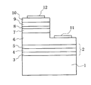
最後に、GaN膜6〜p型のGaN膜10の一部分をエッチングにより除去し、GaN膜6の一部の表面を露出させる。そして、GaN膜6の露出した表面上に電極11を形成するとともに、低抵抗のGaN膜10の表面上にも電極12を形成して、目的とする発光デバイスを得る。
【0056】
また、上述した発光デバイスの変型例として、以下に示すような発光デバイスを例示することもできる。図5に示すようにバッファ層2の表面に、先ず,Al組成が0.8のn型のAlGaInN膜6を1〜2μmの膜厚に形成する。このAlGaInN膜6は、デバイス多層膜中で最大の膜厚を有するものであるが、本発明においては、バッファ層2のAl組成の最小値を、この膜厚最大のAlGaInN膜のAl組成以上とする。
【0057】
さらに、図5に示すように、AlGaInN膜6の上に、Al組成が0.5のn型のAlGaInN膜7をほぼ0.5μmの膜厚に成膜する。この場合において、AlGaInN膜6及び7間におけるAl組成の差が10%以上となっているので、AlGaInN膜6内に比較的多量の転位を含んでいたとしても、この転位がAlGaInN膜7に伝搬する割合が減少する。
【0058】
次いで、AlGaInN膜7上に発光層としてAl組成が0.4のAlGaInN膜8をほぼ0.1μmの膜厚に成膜する。この発光層であるAlGaInN膜7の上に、Al組成が0.5のp型のAlGaInN膜9をほぼ0.5μmの膜厚に成膜し、Al組成が0.1以下の低抵抗のp型のAlGaInN膜10をほぼ0.5μmの膜厚に成膜する。
【0059】
最後に、AlGaInN膜6〜10の一部分をエッチングにより除去してn型のAlGaInN膜6の一部の表面を露出させ、そこに電極11を形成すると共に低抵抗のp型AlGaInN膜10の上にも電極12を形成する。
【0060】
図6は、本発明によるフォトニックデバイスの一実施例である紫外線に感度を有するpinタイプのフォトダイオードを製造する一例の工程を示すものである。図6に示すように基板1の表面に、AlN膜3、Al0.985Ga0.015N膜4およびAl0.85
Ga0.15N膜5より成るバッファ層2を形成した後、このバッファ層2の表面に、先ず,Al組成が0.5のn型のAlGaInN膜6を1〜2μmの膜厚に形成する。
【0061】
このAlGaInN膜6は、デバイス多層膜中で最大の膜厚を有するものであるが、本発明においては、バッファ層2のAl組成の最小値を、この膜厚最大のAlGaInN膜6のAl組成以上とする。
【0062】
さらに、図6に示すように、AlGaInN膜6の上に、Al組成が0.5のnon−dopeのAlGaInN膜7をほぼ100Åの膜厚に成膜し、さらに、Al組成が0.15のp型のAlGaInN膜8をほぼ100nmの膜厚に成膜し、最後に、AlGaInN膜6〜8の一部分をエッチングにより除去してn型のAlGaInN膜6の一部の表面を露出させ、そこに電極11を形成すると共にp型AlGaInN膜8の上にも電極12を形成してpinタイプのフォトダイオードを完成する。
【0063】
図6に示すフォトダイオードの受光面は電極12を透明電極として図の上側とすることもできるし、基板1を透明とする場合には基板側とすることもできる。
【0064】
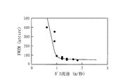
上述したように、バッファ層2の成膜条件として、上記(1)式で求めた平均ガス流速を1m/秒以上とする。図7は、横軸に平均ガス流速を取り、縦軸に結晶性を表すX線ロッキングカーブの半値巾(FWHM)を取って示すものである。図7に示されたプロットは、種々のガス流量、反応管断面積、及び反応管内圧力から(1)式を用いて導出した平均ガス流速のデータである。図7から明らかなように、平均ガス流速を1m/秒以上とすることにより、半値巾FWHMが90arcsec以下となり、良好な結晶性を有するバッファ層2が形成できることが確認されている。
【0065】
本発明は上述した実施例にのみ限定されるものではなく、幾多の変更や変型が可能である。例えば、上述した実施例では基板本体を、C面のサファイアを以て形成したが、サファイアの他の結晶面、ZnOなどの酸化物結晶、SiC、Si、GaAs、GaNなどの半導体結晶で形成された基板本体を用いることもできる。さらに、上述した実施例では、紫外線を放射する発光ダイオードあるいはpinタイプのフォトダイオードとしたが、青色などの他の色の光を発生する発光ダイオードや、レーザダイオードなどの他の発光デバイス、あるいはショットキータイプのフォトダイオードなどの他の受光デバイスとすることもできる。
【0066】
また、上述した実施例では、サファイア基板本体の上にバッファ層をエピタキシャル成長により成膜し、さらにその上にデバイス多層膜をエピタキシャル成長により成膜したが、基板本体上に100μm程度の厚みでバッファ層を形成した後、基板本体を除去し、さらにその後にデバイス多層膜を成膜することもできる。
【0067】
上述したように、本発明によるフォトニックデバイスの製造方法においては、クラックの発生がなく、良好な結晶性を有するAlxGayInzN(x+y+z=1,x,y,z≧0)のバッファ層の上に、良好な結晶性を有するAlxGayInzN(x+y+z=1,x,y,z≧0)のデバイス多層膜を成膜したフォトニックデバイスを提供することができ、特に青色光から紫外線に亘る短波長の光を発光あるいは受光し、効率が良好で、電気的な特性も良好なフォトニックデバイスを実現することができる。
【図面の簡単な説明】
【図1】AlNバッファ層の膜厚と、結晶性との関係を示すグラフである。
【図2】AおよびBは、AlNバッファ層の膜厚と、格子定数aおよびbとの関係を示すグラフである。
【図3】AlNの結晶構造を模式的に示す線図である。
【図4】発光デバイスとして構成した本発明によるフォトニックデバイスの一実施例を製造する一例の工程を示す断面図である。
【図5】同じく図4の工程の次の工程を示す断面図である。
【図6】発光デバイスとして構成した本発明によるフォトニックデバイスの一実施例の構成を示す断面図である。
【図7】バッファ層成膜時における平均ガス流速とその結晶性との関係を示すグラフである。
【符号の説明】
1 C−面サファイア基板本体、 2 バッファ層、 3 AlN膜、 4、5AlGaN膜、 6、7 n型AlGaInN膜、 8 発光層、 9 p型AlGaInN膜、 10 低抵抗p型AlGaInN膜、 11、12 電極[0001]
The present invention relates to a light-emitting device, a light-receiving device, or the like configured by depositing a multilayer thin film of III-V nitride semiconductor material by epitaxial growth.Photonic device manufacturing methodIt is about.
[0002]
[Prior art]
As the III-V nitride semiconductor material described above, AlxGayInzN (x + y + z = 1, x, y, z ≧ 0) is widely used. Such AlxGayInzThe N (x + y + z = 1, x, y, z ≧ 0) film is formed by epitaxial growth by MOCVD, but as a group III source gas, TMA (trimethylaluminum) is used when forming an AlN film. ), TMG (trimethylgallium) is used when forming the GaN film, and trimethylindium is used when forming the InN film. Is NH3(Ammonia) is generally used, and the carrier gas is N2And H2Is used.
[0003]
Generally, AlxGayInzWhen forming an N (x + y + z = 1, x, y, z ≧ 0) film, a group III-V nitride semiconductor thin film having a desired composition is controlled by controlling the supply ratio of the group III source gas described above. Although the band gap Eg of AlN is 6.2 eV, the band gap of GaN is 3.4 eV, the band gap of InN is 1.9 eV, the emission wavelength λ and the band gap Eg Since there is a relationship of λ = 1240 / Eg between them, the wavelengths of light emitted from the light emitting devices using these nitride semiconductor materials are approximately 200 nm, 365 nm, and 653 nm, respectively. Further, in a light receiving device using such a nitride semiconductor material, light having a wavelength equal to or shorter than the above-described wavelength can be detected.
[0004]
Further, the composition of the nitride semiconductor material thin film to be formed can be controlled by adjusting the mixing ratio of the group III source gas described above, whereby a desired emission wavelength or light reception wavelength can be obtained. . For example, when TMA and TMG are mixed, AlxGa1-xWhen an N mixed crystal thin film is formed, the band gap Eg can be approximated to 6.2x + 3.4 (1-x), and the emission wavelength λ is also 1240 / {6.2x + 3.4 (1-x)}. Can be approximated. Therefore, for example, when x = 0.3, the emission wavelength λ is approximately 292 nm. Similarly, the light receiving wavelength has sensitivity in a wavelength region equal to or shorter than the wavelength defined by the above-described formula.
[0005]
As mentioned above, Al is a group III-V nitride semiconductor material.xGayInzIn manufacturing a light emitting diode having an N (x + y + z = 1, x, y, z ≧ 0) multilayer thin film structure, Al is directly formed on the C-plane of the sapphire substrate by MOCVD.xGayInzWhen epitaxially growing N thin film, AlxGayInzThe N thin film includes many defects, has very poor crystallinity, and has very low efficiency.
[0006]
Therefore, Al on the surface of the sapphire substratexGayInzIt has been proposed that a device multilayer film of N (x + y + z = 1, x, y, z ≧ 0) is not directly formed, but a GaN film acting as a buffer layer is formed by epitaxial growth of low temperature CVD. By interposing a buffer layer formed by epitaxial growth by such low temperature CVD, a difference of 10% or more between the lattice constant of the sapphire substrate and the lattice constant of the device multilayer film is compensated, and the device has good crystallinity. A multilayer film can be formed. As a buffer layer, it has also been proposed to form an AlN film instead of a GaN film by low-temperature CVD epitaxial growth.
[0007]
Conventional light emitting devices are mainly those with a long emission wavelength λ of 400 nm or more, but as described above, it is necessary to increase the Al composition in the device multilayer film in order to emit short wavelength blue light or ultraviolet light. There is. Also, in the conventional light emitting device from green to blue, it is necessary to increase the Al composition other than the light emitting layer in order to efficiently confine the light emitting layer. Thus, aluminum rich AlxGayInzWhen a device multilayer film of N (x + y + z = 1, x, y, z ≧ 0) is formed on the buffer layer formed by epitaxial growth by low-temperature CVD as described above, cracks are generated or the crystallinity is remarkably increased. It will deteriorate.
[0008]
The reason is that Al is rich in aluminum (small lattice constant)xGayInzN (x + y + z = 1, x, y, z ≧ 0) When a thin film is formed on a buffer layer having a small aluminum composition (large lattice constant), a tensile stress is generated in the device multilayer film, and cracks are generated. Rich AlxGayInzThe lateral growth rate of the N (x + y + z = 1, x, y, z ≧ 0) thin film is slow, and the low-temperature buffer layer with poor crystallinity is made of Al.xGayInzThis is considered to be because the improvement of the crystallinity of the device multilayer film of N (x + y + z = 1, x, y, z ≧ 0) is inhibited. Even in the ultraviolet light receiving device, there is a problem that the light receiving sensitivity is deteriorated due to the deterioration of the crystallinity.
[0009]
In order to eliminate such drawbacks, for example, in Japanese Patent Laid-Open No. 9-64477, Al is formed on a sapphire substrate.xGa1-xAn N (1 ≧ x> 0) film is formed as a buffer layer, and an aluminum-rich Al film is formed thereon.xGayInzThere has been proposed a light-emitting device in which an N (x + y + z = 1, x, y, z ≧ 0) device multilayer film is formed.
[0010]
Furthermore, Japanese Patent Laid-Open No. 5-291618 discloses Ga on the sapphire substrate body.1-xyInxAlyN (1 ≧ x ≧ 0, 1 ≧ y ≧ 0) thin film is formed, and its composition x and / or y is changed to finally form Ga1-abInaAlbA buffer layer is formed so as to have a composition of N (1 ≧ a ≧ 0, 1 ≧ b ≧ 0).1-abInaAlbA light emitting device in which a device multilayer film composed of N (1 ≧ a ≧ 0, 1 ≧ b ≧ 0) is formed is disclosed.
[0011]
[Problems to be Solved by the Invention]
In the technique described in Japanese Patent Laid-Open No. 9-64477 described above, by using a high-temperature AlGaN buffer layer, an aluminum-rich Al layer is formed thereon.xGayInzA device multilayer film of N (x + y + z = 1, x, y, z ≧ 0) can be formed with good crystallinity, and the occurrence of cracks in the device multilayer film can also be suppressed.
[0012]
However, it is necessary to increase the film formation temperature when forming the AlGaN buffer layer to 1300 ° C. or higher. Moreover, it is necessary to anneal at a high temperature of about 1500 ° C. after the formation of the AlGaN buffer layer. As described above, since a high-temperature treatment is required, the burden on the heater of the MOCVD apparatus becomes very large, maintenance becomes very troublesome, and there is a disadvantage that the manufacturing cost increases.
[0013]
In particular, in order to realize a photonic device that emits or receives short-wavelength light as described above, an aluminum-rich Al layer is used in the device multilayer film.xGayInzN (x + y + z = 1, x, y, z ≧ 0) layers need to be provided, but since the growth rate in the vertical and horizontal directions of such an aluminum-rich layer is slow, the film forming temperature needs to be very high. There is a problem that the burden on the apparatus becomes particularly large.
[0014]
Here, when the film forming temperature is lowered to about 1200 ° C., a crack occurs in the buffer layer with a film thickness of about 0.3 μm, and the crystallinity of the buffer layer is insufficient, and the device has good crystallinity. A multilayer film cannot be formed.
[0015]
In the technique described in the above-mentioned Japanese Patent Application Laid-Open No. 5-291618, Ga1-xyInxAlyN (1.gtoreq.x.gtoreq.0, 1.gtoreq.y.gtoreq.0) The composition x and / or y of the buffer layer is changed and finally Ga.1-abInaAlbN (1 ≧ a ≧ 0, 1 ≧ b ≧ 0), and on top of that, Ga1-abInaAlbSince the device multilayer film composed of N (1 ≧ a ≧ 0, 1 ≧ b ≧ 0) is formed, the crystallinity of the device multilayer film is improved and the generation of cracks is effectively suppressed. Furthermore, since the film formation temperature of the buffer layer is as low as about 700 ° C., the load on the heater is also reduced.
[0016]
However, in this known technique, the composition is controlled so that the buffer layer and the device multilayer film are continuously connected. In this way, when the composition is continuously connected at the interface between the buffer layer and the device multilayer film, current leakage from the device multilayer film to the buffer layer occurs, and loss due to resistance occurs at that part, There is a disadvantage that efficiency is lowered.
[0017]
Accordingly, an object of the present invention is to provide Al having excellent crystallinity without cracks on a sapphire substrate, SiC substrate, GaN substrate, or the like.xGayInzN (x + y + z = 1, x, y, z ≧ 0) buffer layer and Al having excellent crystallinity without cracks formed thereon by epitaxial growthxGayInzIt is an object of the present invention to provide a photonic device having an N (x + y + z = 1, x, y, z ≧ 0) device multilayer film and a method capable of manufacturing such a photonic device.
[0018]
In order to achieve the above object, the present invention provides:
Al deposited on one surface of sapphire, ZnO, SiC, Si, GaAs, GaN, etc.xGayInzN (x + y + z = 1, x, y, z ≧ 0) buffer layer and Al deposited on the surface of the buffer layer by epitaxial growthxGayInzA method of manufacturing a photonic device comprising N (x + y + z = 1, x, y, z ≧ 0) device multilayer film,
In the buffer layer, the Al composition of the smallest Al composition is at least the Al composition of the layer with the largest film thickness in the device multilayer film,
The device multilayer film is formed by epitaxial growth by MOCVD at a substrate surface temperature lower than the film formation temperature of the buffer layer,
The substrate surface temperature during film formation of the buffer layer is 1100 ° C. or more and less than 1300 ° C.,
The present invention relates to a photonic device manufacturing method, wherein an average gas flow rate during film formation of the buffer layer is 1 m / second or more.
[0019]
Obtained by such a method of the present inventionThe photonic device can be configured as a light emitting device or a light receiving device. Furthermore, the present inventionPhotonic device manufacturing methodIn the preferred embodiment, the composition of the layer having the maximum Al composition in the device multilayer film can be suitably used for a light emitting device for short-wavelength light emission, a light-receiving device for short-wavelength light reception, or the like.xGayInzN (x + y + z = 1, 1.0 ≧ x ≧ 0.3) is desirable. Also, the Al composition in the buffer layer with the smallest Al composition is changed to AlxGayInzN (x + y + z = 1, 1.0 ≧ x ≧ 0.5) is preferable, and 1.0 ≧ x ≧ 0.7 is more preferable.
[0020]
Furthermore, according to the inventionPhotonic device manufacturing methodIn a preferred embodiment, the portion of the buffer layer closest to the substrate body has a composition of AlN. As a result, the degree of freedom of composition in the buffer layer is increased, so that a device multilayer film having desired characteristics can be easily realized.
[0021]
The buffer layer preferably has an interface having an Al composition difference of 10 atomic% or more. Similarly, it is preferable that the device multilayer film and the buffer layer have an interface having an Al composition difference of 10 atomic% or more. By providing a step having an Al composition between adjacent layers in this way, in particular, dislocations do not propagate upward beyond the Al step. Therefore, the amount of dislocation in the upper portion of the Al composition step can be suppressed, and a device multilayer film excellent in crystallinity can be obtained.
[0023]
In the production method according to the present invention,The buffer layer is formed by epitaxial growth by MOCVD at a substrate surface temperature higher than the film formation temperature of the device multilayer film. Specifically, the deposition temperature of the buffer layer is 1100 ° C. or higherAnd
[0024]
Also, the AlxGayInzThe flow rate ratio of hydrogen gas and nitrogen gas (hydrogen gas / nitrogen gas) used as a carrier gas when forming a buffer layer having a composition of N (x + y + z = 1, x, y, z ≧ 0) is determined as the device multilayer. It is preferable that the flow rate ratio of hydrogen gas and nitrogen gas (hydrogen gas / nitrogen gas) used as a carrier gas when the film is formed be larger than the hydrogen gas / nitrogen gas.
[0025]
Also, the AlxGayInzFlow rate ratio of Group V source gas to Group III source gas used when forming a buffer layer having a composition of N (x + y + z = 1, x, y, z ≧ 0) (Group V source gas / Group III source gas) Is preferably smaller than the flow rate ratio of the group V source gas used for forming the device multilayer film to the group III source gas (group V source gas / group III source gas). Here, the flow rate of the group III source gas is calculated from the saturated vapor pressure on the assumption that polymerization such as dimerization has not occurred.
[0026]
Further, when a group III source gas containing Al and a group V source gas are used, the average gas flow rate including the source gas in the reaction tube at the top of the substrate is 1 m / sec or more.Be. The average gas flow rate in this case is represented by the following formula (1).
[0027]
[Expression 1]
{Total gas flow rate converted to 0 ° C (L / min) / 60 × 103× Reaction tube cross-sectional area at the top center of the substrate (m2)}
× {760 / pressure in reaction tube (Torr)} (1)
[0028]
That is, the average gas flow rate increases as the total gas flow rate increases, the reaction tube cross-sectional area decreases, or the reaction tube internal pressure decreases. Therefore, the reaction of the source gas in the gas phase can be suppressed, and the crystallinity of the buffer layer can be improved more effectively.
[0029]
Furthermore, according to the inventionPhotonic device manufacturing methodIn this case, the buffer layer is supported by a substrate body such as sapphire, SiC, or GaN, and a device multilayer film can be formed thereon, but after the buffer layer is formed with a thickness of about 100 μm, The substrate body can also be removed.
[0030]
According to the invention described abovePhotonic device manufacturing methodIn the device multilayer film, the composition of the layer with the largest Al composition is Al.xGayInzN (x + y + z = 1, 1.0 ≧ x ≧ 0.3) is preferable. Since the main purpose of the present invention is to realize a photonic device in the ultraviolet region, the Al composition x of the light emitting layer in the device multilayer film is large.
[0031]
Therefore, the Al composition of the film stacked around the periphery is further increased. For example, assuming an ultraviolet light having an emission wavelength λ of about 300 nm, the Al composition x is 0.3. Therefore, in the present invention, the composition of the layer having the largest Al composition in the device multilayer film is expressed as Al.xGayInzN (x + y + z = 1, 1.0 ≧ x ≧ 0.3).
[0032]
Furthermore, in the present invention, the Al composition in the buffer layer having the smallest Al composition is set to be equal to or greater than the Al composition of the maximum thickness layer in the device multilayer film. This requirement is a condition for suppressing cracks that may occur in the film. In the device multilayer film, the largest stress is generated in the layer portion having the maximum film thickness, and the portion having the highest probability of occurrence of cracks. When tensile stress is generated in the maximum film thickness portion, cracks are generated. In order to suppress the occurrence of cracks by generating compressive stress in this layer, it is necessary to make the Al composition of the buffer layer larger than this layer.
[0033]
Further, in the present invention, the Al composition x of the buffer layer is configured so that the value of the Al composition ratio x decreases continuously or stepwise from the substrate body side toward the device multilayer film. The requirements are the most characteristic of the present invention.
[0034]
An object of the present invention is to form a buffer layer having good crystallinity at a low temperature of about 1200 ° C. without using a conventional high temperature of 1300 ° C. or higher. Al with good crystallinityxGayInzIn order to form an N (x + y + z = 1, x, y, z ≧ 0) buffer layer, it is necessary to increase the thickness of the buffer image from about 1 μm to about 2 μm.
[0035]
However, there is a problem that cracks occur when the thickness of the buffer layer is increased in this way. The reason is that tensile stress is generated when the buffer layer is formed, and the thicker the buffer layer, the larger the lattice constant and the easier the cracks are. This will be described in detail later.
[0036]
In order to solve such a problem, it is sufficient to change the material of the buffer layer to a material having a large lattice constant before a crack is generated. As mentioned above, Al in the buffer layerxGayInzSince the lattice constant is increased by reducing the Al composition of N (x + y + z = 1, x, y, z ≧ 0), stress inside the buffer layer can be prevented, and as a result, about 1200 ° C. Even at low temperatures, the thickness of the buffer layer can be increased without generating cracks, and the crystallinity can be improved. In addition, by adding Ga to the buffer layer, there is a secondary effect of promoting the growth rate in the lateral direction, so there is also a dislocation suppression effect.
[0037]
As described above, in the present invention, it is preferable to form the buffer layer at a higher substrate surface temperature than the device multilayer film, but the buffer layer has a higher Al composition than the device multilayer film. This is because a high temperature is required for film formation. Therefore, the buffer layer of the present invention should also be referred to as a high temperature buffer layer.
[0038]
As described above, a tensile stress is generated when the buffer layer is formed, so that cracks are easily generated. This will be further described. In FIG. 1, the horizontal axis indicates the film thickness of the AlN portion of the buffer layer on the substrate body side, and the vertical axis indicates the half width (FWHM) of the X-ray rocking curve of the (002) peak, which is a measure of the crystallinity of the AlN film. Is shown. It can be seen that the full width at half maximum decreases as the thickness of the AlN film increases, and the crystallinity improves.
[0039]
2A and 2B show the film thickness of the AlN film on the horizontal axis and the lattice constants a and b of the AlN film on the vertical axis. Here, as shown in FIG. 3, the lattice constants a and b correspond to the length and height of one side of the hexagonal column bottom surface of the AlN crystal formed on the C-plane of the sapphire substrate body, respectively. . In these drawings, a thick solid line indicates an ideal lattice constant of the AlN film. As can be seen from these graphs, the lattice constant a increases and the lattice constant c decreases as the thickness of the AlN film increases.
[0040]
From the above, it can be seen that the crystallinity is improved and the in-plane lattice constant a is increased as the thickness of the AlN film is increased. That is, it can be seen that as the thickness of the AlN film increases, tensile stress acts in the surface and cracks are likely to occur.
[0041]
Also in the production method of the present invention, it is preferable that the buffer layer has an interface having an Al composition difference of 10 atomic% or more. Similarly, it is preferable that the device multilayer film and the buffer layer have an interface having an Al composition difference of 10 atomic% or more. Thereby, as described above, a device multilayer film having excellent crystallinity can be manufactured.
[0042]
DETAILED DESCRIPTION OF THE INVENTION
4 and 5 show an exemplary process for manufacturing an ultraviolet light emitting device which is an embodiment of the photonic device according to the present invention. C-plane sapphire (Al2O3) The
[0043]
That is, the flow rate ratio of hydrogen gas and nitrogen gas used as carrier gas (H2Flow rate / N2The flow rate is infinite. Further, the ratio of the group V source gas flow rate to the group III source gas flow rate (group V source gas flow rate / group III source gas flow rate) is 450, and the supply amount of the source gas is set so that the film forming rate is 1 μm / hour. Controlled. In this case, the cross-sectional area of the reaction tube at the upper center of the substrate is 5 × 10.-3m2Therefore, when the average gas flow rate is calculated from the equation (1), it becomes 1.7 m / sec.
[0044]
In this example, a portion of the
[0045]
Here, the gas flow rate is changed from the deposition conditions of the
[0046]
In this case, the rocking curve half-width (FWHM) of the (002) peak of the buffer layer was 50 arcsec. Further, since the difference in Al composition between the
[0047]
Next, a device multilayer film is formed on the surface of the
[0048]
The substrate surface temperature during film formation is 1050 ° C., which is lower than the substrate surface temperature 1200 ° C. when the
[0049]
In the present invention, as described above, the flow rate ratio of the hydrogen gas and the nitrogen gas used as the carrier gas is set to be equal to or less than the flow rate ratio when the
[0050]
Further, the flow rate ratio of the Group V source gas and the Group III source gas when forming the
[0051]
Here, also in the device multilayer film formation, if the flow rate of the hydrogen gas is increased and the flow rate ratio of the group V source gas and the group III source gas is reduced, the light emission characteristics may be deteriorated. The reason is AlxGayInzThis is because when the Ga and In concentrations in the N film are increased, etching with hydrogen gas is more likely to occur, and as a result, the crystallinity of the film is deteriorated. For this reason, it is considered that the light emission characteristics and electrical characteristics of the entire device multilayer film deteriorate.
[0052]
The case where a light emitting device as a photonic device is formed will be described below. As shown in FIG. 5, first, an n-
[0053]
This
[0054]
Next, n-type Al is formed on the GaN film 6.0.10Ga0.90
[0055]
Finally, a part of the
[0056]
Moreover, the light emitting device as shown below can also be illustrated as a modified example of the light emitting device described above. As shown in FIG. 5, an n-
[0057]
Further, as shown in FIG. 5, an n-
[0058]
Next, an
[0059]
Finally, a part of the
[0060]
FIG. 6 shows an example of a process for manufacturing a pin type photodiode having sensitivity to ultraviolet rays, which is an embodiment of the photonic device according to the present invention. As shown in FIG. 6, the
Ga0.15After the
[0061]
The
[0062]
Further, as shown in FIG. 6, a
[0063]
The light receiving surface of the photodiode shown in FIG. 6 can be the upper side of the figure with the
[0064]
As described above, the average gas flow rate obtained by the above equation (1) is set to 1 m / second or more as the film forming condition of the
[0065]
The present invention is not limited to the above-described embodiments, and many changes and modifications can be made. For example, in the above-described embodiments, the substrate body is formed of C-plane sapphire, but the substrate is formed of another crystal surface of sapphire, an oxide crystal such as ZnO, or a semiconductor crystal such as SiC, Si, GaAs, or GaN. The main body can also be used. Further, in the above-described embodiments, a light emitting diode or a pin type photodiode that emits ultraviolet rays is used. However, a light emitting diode that generates light of other colors such as blue, another light emitting device such as a laser diode, or a shot. Other light receiving devices such as a key type photodiode may be used.
[0066]
In the above-described embodiment, the buffer layer is formed on the sapphire substrate body by epitaxial growth, and further the device multilayer film is formed on the sapphire substrate body by epitaxial growth, but the buffer layer is formed on the substrate body with a thickness of about 100 μm. After the formation, the substrate body can be removed, and then a device multilayer film can be formed.
[0067]
As mentioned above, according to the present inventionPhotonic device manufacturing methodIn Al, there is no generation of cracks and good crystallinity.xGayInzAl having good crystallinity on a buffer layer of N (x + y + z = 1, x, y, z ≧ 0)xGayInzIt is possible to provide a photonic device in which a device multilayer film of N (x + y + z = 1, x, y, z ≧ 0) is formed. In particular, it emits or receives light having a short wavelength ranging from blue light to ultraviolet light. Can be realized, and a photonic device with good electrical characteristics can be realized.
[Brief description of the drawings]
FIG. 1 is a graph showing the relationship between the film thickness of an AlN buffer layer and crystallinity.
FIGS. 2A and 2B are graphs showing the relationship between the thickness of an AlN buffer layer and lattice constants a and b. FIGS.
FIG. 3 is a diagram schematically showing the crystal structure of AlN.
FIG. 4 is a cross-sectional view showing an example process for manufacturing an embodiment of a photonic device according to the present invention configured as a light emitting device.
5 is a cross-sectional view showing a step subsequent to the step in FIG. 4; FIG.
FIG. 6 is a cross-sectional view showing a configuration of an embodiment of a photonic device according to the present invention configured as a light emitting device.
FIG. 7 is a graph showing the relationship between the average gas flow rate and the crystallinity during buffer layer deposition.
[Explanation of symbols]
1 C-plane sapphire substrate body, 2 buffer layer, 3 AlN film, 4, 5 AlGaN film, 6, 7 n-type AlGaInN film, 8 light-emitting layer, 9 p-type AlGaInN film, 10 low resistance p-type AlGaInN film, 11, 12 electrode
Claims (6)
前記バッファ層中の、Al組成が最少の部分のAl組成を、前記デバイス多層膜中の少なくとも最大膜厚の層のAl組成以上とし、
前記デバイス多層膜を、前記バッファ層の成膜温度よりも低い基板表面温度でMOCVD法によりエピタキシャル成長させて形成し、
前記バッファ層の成膜時の基板表面温度は1100℃以上1300℃未満とするとともに、
前記バッファ層の成膜時における平均ガス流量が1m/秒以上であることを特徴とする、フォトニックデバイスの製造方法。Al x Ga y In z N (x + y + z = 1, x, y, z ≧ 0) buffer layer deposited on one surface of sapphire, ZnO, SiC, Si, GaAs, GaN or the like as a substrate body; A method of manufacturing a photonic device comprising an Al x Ga y In z N (x + y + z = 1, x, y, z ≧ 0) device multilayer film deposited and formed on the surface of the buffer layer by epitaxial growth,
In the buffer layer, the Al composition of the portion having the smallest Al composition is at least the Al composition of the layer with the largest film thickness in the device multilayer film,
The device multilayer film is formed by epitaxial growth by MOCVD at a substrate surface temperature lower than the film formation temperature of the buffer layer,
The substrate surface temperature during film formation of the buffer layer is 1100 ° C. or more and less than 1300 ° C.,
The method for producing a photonic device, wherein an average gas flow rate during film formation of the buffer layer is 1 m / second or more.
Priority Applications (5)
| Application Number | Priority Date | Filing Date | Title |
|---|---|---|---|
| JP2001114065A JP3626423B2 (en) | 2000-05-22 | 2001-04-12 | Photonic device manufacturing method |
| US09/854,925 US6495894B2 (en) | 2000-05-22 | 2001-05-14 | Photonic device, a substrate for fabricating a photonic device, a method for fabricating the photonic device and a method for manufacturing the photonic device-fabricating substrate |
| EP01112409.6A EP1160882B1 (en) | 2000-05-22 | 2001-05-21 | Method for manufacturing a photonic device |
| KR1020010027650A KR20010107604A (en) | 2000-05-22 | 2001-05-21 | A photonic device, a substrate for fabricating a photonic device, a method for fabricating the photonic device and a method for manufacturing the photonic device-fabricating substrate |
| CNB011372893A CN1193439C (en) | 2000-05-22 | 2001-05-22 | Luminous element, substrate for mfg. same, and mfg. method for mfg. them |
Applications Claiming Priority (5)
| Application Number | Priority Date | Filing Date | Title |
|---|---|---|---|
| JP2000149190 | 2000-05-22 | ||
| JP2000-149190 | 2000-05-22 | ||
| JP2000-293763 | 2000-09-27 | ||
| JP2000293763 | 2000-09-27 | ||
| JP2001114065A JP3626423B2 (en) | 2000-05-22 | 2001-04-12 | Photonic device manufacturing method |
Publications (2)
| Publication Number | Publication Date |
|---|---|
| JP2002176196A JP2002176196A (en) | 2002-06-21 |
| JP3626423B2 true JP3626423B2 (en) | 2005-03-09 |
Family
ID=27343445
Family Applications (1)
| Application Number | Title | Priority Date | Filing Date |
|---|---|---|---|
| JP2001114065A Expired - Lifetime JP3626423B2 (en) | 2000-05-22 | 2001-04-12 | Photonic device manufacturing method |
Country Status (1)
| Country | Link |
|---|---|
| JP (1) | JP3626423B2 (en) |
Families Citing this family (11)
| Publication number | Priority date | Publication date | Assignee | Title |
|---|---|---|---|---|
| WO2002013245A1 (en) * | 2000-08-04 | 2002-02-14 | The Regents Of The University Of California | Method of controlling stress in gallium nitride films deposited on substrates |
| JP3768943B2 (en) | 2001-09-28 | 2006-04-19 | 日本碍子株式会社 | Group III nitride epitaxial substrate, group III nitride device epitaxial substrate, and group III nitride device |
| JP4063548B2 (en) | 2002-02-08 | 2008-03-19 | 日本碍子株式会社 | Semiconductor light emitting device |
| EP1400835B1 (en) | 2002-09-17 | 2011-11-16 | Nippon Telegraph And Telephone Corporation | Semiconductor optical modulator and laser with such optical modulator |
| JP4189386B2 (en) * | 2005-01-27 | 2008-12-03 | ローム株式会社 | Method for growing nitride semiconductor crystal layer and method for producing nitride semiconductor light emitting device |
| KR100831713B1 (en) | 2006-11-02 | 2008-05-22 | 삼성전기주식회사 | Nitride semiconductor light emitting diode |
| JP2008198705A (en) * | 2007-02-09 | 2008-08-28 | Showa Denko Kk | Method for manufacturing group iii nitride semiconductor light-emitting device, group iii nitride semiconductor light-emitting device, and lamp |
| JP5274785B2 (en) * | 2007-03-29 | 2013-08-28 | 日本碍子株式会社 | Method for forming AlGaN crystal layer |
| JP5665036B2 (en) * | 2009-03-10 | 2015-02-04 | 浜松ホトニクス株式会社 | Method for producing compound semiconductor layer structure |
| KR20130137295A (en) * | 2012-06-07 | 2013-12-17 | 엘지이노텍 주식회사 | Light emitting device and light emitting device package |
| CN114203865B (en) * | 2021-12-07 | 2023-08-01 | 宁波安芯美半导体有限公司 | Preparation method of aluminum nitride epitaxial wafer based on sapphire substrate |
-
2001
- 2001-04-12 JP JP2001114065A patent/JP3626423B2/en not_active Expired - Lifetime
Also Published As
| Publication number | Publication date |
|---|---|
| JP2002176196A (en) | 2002-06-21 |
Similar Documents
| Publication | Publication Date | Title |
|---|---|---|
| US7998773B2 (en) | Method of growing semiconductor heterostructures based on gallium nitride | |
| US6495894B2 (en) | Photonic device, a substrate for fabricating a photonic device, a method for fabricating the photonic device and a method for manufacturing the photonic device-fabricating substrate | |
| JP4539752B2 (en) | Method for forming quantum well structure and method for manufacturing semiconductor light emitting device | |
| JP3728332B2 (en) | Compound semiconductor light emitting device | |
| JP5048236B2 (en) | Semiconductor light emitting device and method for manufacturing semiconductor light emitting device | |
| US7550368B2 (en) | Group-III nitride semiconductor stack, method of manufacturing the same, and group-III nitride semiconductor device | |
| US8183071B2 (en) | Method for producing nitride semiconductor optical device and epitaxial wafer | |
| JP2001160627A (en) | Group iii nitride compound semiconductor light emitting element | |
| JPWO2008153130A1 (en) | Nitride semiconductor light emitting device and method for manufacturing nitride semiconductor | |
| JP4724901B2 (en) | Manufacturing method of nitride semiconductor | |
| JP4131618B2 (en) | Manufacturing method of substrate for photonic device | |
| JP2000091234A (en) | Manufacture of iii-v nitride compound semiconductor | |
| JP3626423B2 (en) | Photonic device manufacturing method | |
| JP2009023853A (en) | Group iii-v nitride semiconductor substrate, method for manufacturing the same, and group iii-v nitride semiconductor device | |
| JPH11145063A (en) | Semiconductor device having gallium nitride semiconductor layer and its manufacture | |
| JP2012204540A (en) | Semiconductor device and method of manufacturing the same | |
| JP2010199236A (en) | Light emitting element producing method and light emitting element | |
| JP2004014587A (en) | Nitride compound semiconductor epitaxial wafer and light emitting element | |
| KR101137513B1 (en) | Nitride semiconductor light emitting device and method for manufacturing thereof | |
| JP2009088230A (en) | Semiconductor light-emitting element and manufacturing method thereof | |
| JP2006324680A (en) | Crystal film, crystal substrate, and semiconductor device | |
| KR20060066872A (en) | Substrate for semiconductor light-emitting device and nitride semiconductor light-emitting device and method for manufacturing the same | |
| JP3767534B2 (en) | Light emitting device | |
| JP3556593B2 (en) | Compound semiconductor light emitting device and method of manufacturing the same | |
| JP2011223043A (en) | Semiconductor light-emitting device and method of manufacturing the semiconductor light-emitting device |
Legal Events
| Date | Code | Title | Description |
|---|---|---|---|
| A977 | Report on retrieval |
Free format text: JAPANESE INTERMEDIATE CODE: A971007 Effective date: 20040603 |
|
| A131 | Notification of reasons for refusal |
Free format text: JAPANESE INTERMEDIATE CODE: A131 Effective date: 20040622 |
|
| A521 | Request for written amendment filed |
Free format text: JAPANESE INTERMEDIATE CODE: A523 Effective date: 20040818 |
|
| TRDD | Decision of grant or rejection written | ||
| A01 | Written decision to grant a patent or to grant a registration (utility model) |
Free format text: JAPANESE INTERMEDIATE CODE: A01 Effective date: 20041109 |
|
| A61 | First payment of annual fees (during grant procedure) |
Free format text: JAPANESE INTERMEDIATE CODE: A61 Effective date: 20041202 |
|
| R150 | Certificate of patent or registration of utility model |
Free format text: JAPANESE INTERMEDIATE CODE: R150 Ref document number: 3626423 Country of ref document: JP Free format text: JAPANESE INTERMEDIATE CODE: R150 |
|
| S201 | Request for registration of exclusive licence |
Free format text: JAPANESE INTERMEDIATE CODE: R314201 |
|
| FPAY | Renewal fee payment (event date is renewal date of database) |
Free format text: PAYMENT UNTIL: 20071210 Year of fee payment: 3 |
|
| R350 | Written notification of registration of transfer |
Free format text: JAPANESE INTERMEDIATE CODE: R350 |
|
| FPAY | Renewal fee payment (event date is renewal date of database) |
Free format text: PAYMENT UNTIL: 20081210 Year of fee payment: 4 |
|
| FPAY | Renewal fee payment (event date is renewal date of database) |
Free format text: PAYMENT UNTIL: 20081210 Year of fee payment: 4 |
|
| FPAY | Renewal fee payment (event date is renewal date of database) |
Free format text: PAYMENT UNTIL: 20091210 Year of fee payment: 5 |
|
| FPAY | Renewal fee payment (event date is renewal date of database) |
Free format text: PAYMENT UNTIL: 20091210 Year of fee payment: 5 |
|
| FPAY | Renewal fee payment (event date is renewal date of database) |
Free format text: PAYMENT UNTIL: 20101210 Year of fee payment: 6 |
|
| FPAY | Renewal fee payment (event date is renewal date of database) |
Free format text: PAYMENT UNTIL: 20111210 Year of fee payment: 7 |
|
| FPAY | Renewal fee payment (event date is renewal date of database) |
Free format text: PAYMENT UNTIL: 20121210 Year of fee payment: 8 |
|
| FPAY | Renewal fee payment (event date is renewal date of database) |
Free format text: PAYMENT UNTIL: 20131210 Year of fee payment: 9 |
|
| EXPY | Cancellation because of completion of term |