EP1296800B1 - Polierkissen mit integriertem optischen sensor - Google Patents
Polierkissen mit integriertem optischen sensor Download PDFInfo
- Publication number
- EP1296800B1 EP1296800B1 EP00947036A EP00947036A EP1296800B1 EP 1296800 B1 EP1296800 B1 EP 1296800B1 EP 00947036 A EP00947036 A EP 00947036A EP 00947036 A EP00947036 A EP 00947036A EP 1296800 B1 EP1296800 B1 EP 1296800B1
- Authority
- EP
- European Patent Office
- Prior art keywords
- polishing pad
- electrical signal
- pad
- optical
- power
- Prior art date
- Legal status (The legal status is an assumption and is not a legal conclusion. Google has not performed a legal analysis and makes no representation as to the accuracy of the status listed.)
- Expired - Lifetime
Links
Images


Classifications
-
- B—PERFORMING OPERATIONS; TRANSPORTING
- B24—GRINDING; POLISHING
- B24B—MACHINES, DEVICES, OR PROCESSES FOR GRINDING OR POLISHING; DRESSING OR CONDITIONING OF ABRADING SURFACES; FEEDING OF GRINDING, POLISHING, OR LAPPING AGENTS
- B24B49/00—Measuring or gauging equipment for controlling the feed movement of the grinding tool or work; Arrangements of indicating or measuring equipment, e.g. for indicating the start of the grinding operation
-
- B—PERFORMING OPERATIONS; TRANSPORTING
- B24—GRINDING; POLISHING
- B24B—MACHINES, DEVICES, OR PROCESSES FOR GRINDING OR POLISHING; DRESSING OR CONDITIONING OF ABRADING SURFACES; FEEDING OF GRINDING, POLISHING, OR LAPPING AGENTS
- B24B37/00—Lapping machines or devices; Accessories
- B24B37/11—Lapping tools
- B24B37/20—Lapping pads for working plane surfaces
- B24B37/205—Lapping pads for working plane surfaces provided with a window for inspecting the surface of the work being lapped
-
- B—PERFORMING OPERATIONS; TRANSPORTING
- B24—GRINDING; POLISHING
- B24B—MACHINES, DEVICES, OR PROCESSES FOR GRINDING OR POLISHING; DRESSING OR CONDITIONING OF ABRADING SURFACES; FEEDING OF GRINDING, POLISHING, OR LAPPING AGENTS
- B24B37/00—Lapping machines or devices; Accessories
- B24B37/005—Control means for lapping machines or devices
- B24B37/013—Devices or means for detecting lapping completion
-
- B—PERFORMING OPERATIONS; TRANSPORTING
- B24—GRINDING; POLISHING
- B24B—MACHINES, DEVICES, OR PROCESSES FOR GRINDING OR POLISHING; DRESSING OR CONDITIONING OF ABRADING SURFACES; FEEDING OF GRINDING, POLISHING, OR LAPPING AGENTS
- B24B49/00—Measuring or gauging equipment for controlling the feed movement of the grinding tool or work; Arrangements of indicating or measuring equipment, e.g. for indicating the start of the grinding operation
- B24B49/12—Measuring or gauging equipment for controlling the feed movement of the grinding tool or work; Arrangements of indicating or measuring equipment, e.g. for indicating the start of the grinding operation involving optical means
Definitions
- the invention relates to a polishing pad for use in performing a polishing operation on a surface of a workpiece, as well as to systems using the polishing pad.
- the present invention is in the field of semiconductor wafer processing, and more specifically relates to a disposable polishing pad for use in a chemical mechanical polishing operation performed on the semiconductor wafers.
- Tang refers to a fiber-optic cable embedded in a polishing pad. This cable is merely a conductor of light. The light source and the detector that do the sensing are located outside of the pad. Nowhere does Tang suggest including a light source and a detector inside the polishing pad.
- fiber-optic decouplers are used to transfer the light in the optical fibers from a rotating component to a stationary component.
- the optical signal is detected onboard a rotating component, and the resulting electrical signal is transferred to a stationary component through electrical slip rings.
- transmitting the electrical signal to a stationary component by means of radio waves, acoustical waves, a modulated light beam, or by magnetic induction.
- U.S. Patent 6,007,408 discloses heat sensor embedded in a polishing pad.
- the heat sensors sense the temperature of the pad, the heat of the polishing slurry and the heat of the wafer preferably at its front side.
- the sensors may be infra red optical sensors.
- an optical sensor that includes a light source and a detector is disposed within a blind hole in the polishing pad so as to face the surface that is being polished. Light from the light source is reflected from the surface being polished and the reflected light is detected by the detector which produces an electrical signal related to the intensity of the light reflected back onto the detector.
- the electrical signal produced by the detector is conducted radially inward from the location of the detector to the central aperture of the polishing pad by a thin conductor concealed between the layers of the polishing pad.
- the disposable polishing pad is removably connected, both mechanically and electrically, to a hub that rotates with the polishing pad.
- the hub contains electronic circuitry that is concerned with supplying power to the optical sensor and with transmitting the electrical signal produced by the detector to non-rotating parts of the system. Because of the expense of these electronic circuits, the hub is not considered to be disposable. After the polishing pad has been worn out from use, it is disposed of, along with the optical sensor and the thin conductor.
- electrical power for operating the electronic circuits within the hub and for powering the light source of the optical sensor may be provided by several techniques.
- the secondary winding of a transformer is included within the rotating hub and a primary winding is located on an adjacent non-rotating part of the polishing machine.
- a solar cell or photovoltaic array is mounted on the rotating hub and is illuminated by a light source mounted on a non-rotating portion of the machine.
- electrical power is derived from a battery located within the hub.
- electrical conductors in the rotating polishing pad or in the rotating hub pass through the magnetic fields of permanent magnets mounted on adjacent non-rotating portions of the polishing machine, to constitute a magneto.
- the electrical signal representing an optical characteristic of the surface being polished is transmitted from the rotating hub to an adjacent stationary portion of the polishing machine by any of several techniques.
- the electrical signal to be transmitted is used to frequency modulate a light beam that is received by a detector located on adjacent non-rotating structure.
- the signal is transmitted by a radio link or an acoustical link.
- the signal may be applied to the primary winding of a transformer on the rotating hub and received by a secondary winding of the transformer located on an adjacent non-rotating portion of the polishing machine. This transformer may be the same transformer that is used for coupling electrical power into the hub, or it can be a different transformer.
- the wafers with which the present invention is used are composite structures that include strata of different materials. Typically, the outermost stratum is polished away until its interface with an underlying stratum has been reached. At that point it is said that the end point of the polishing operation has been reached.
- the polishing pad of the present invention is applicable to detecting transitions from an oxide layer to a silicon layer as well as to transitions from a metal to an oxide or other material.
- the polishing process can be allowed to progress until the optical sensor of the present invention has provided information that permits a determination that the end point has been reached.
- end point sensing is the main objective of the present invention
- other possibilities for using the present invention are under consideration. These include determining how far away the end point is, sampling various areas on a wafer, and mapping the surface of a wafer.
- a single optical sensor is described in the following paragraphs, it is contemplated that for some uses of the invention a number of optical sensors may be included in a polishing pad.
- the present invention involves modifying a conventional polishing pad by embedding within it an optical sensor and other components.
- the unmodified polishing pads are widely available commercially, and the Model IC 1000 made by the Rodel Company of Newark, New Jersey, is a typical unmodified pad. Pads manufactured by the Thomas West Company may also be used. The manner in which these pads are modified in accordance with the present invention and used will be clear from the discussion below.
- the optical sensor of the present invention senses an optical characteristic of the surface that is being polished.
- the optical characteristic of the surface is its reflectivity.
- other optical characteristics of the surface can also be sensed, including its polarization, its absorptivity, and its photoluminescense (if any).
- Techniques for sensing these various characteristics are well known in the optical arts, and typically they involve little more than adding a polarizer or a spectral filter to the optical system. For this reason, in the following discussion the more general term "optical characteristic" is used.
- optical and light as used below include unltraviolet, visible, and infrared types of light.
- radiation and “acoustic” are used in their usual broad sense.
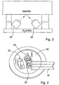
- the polishing pad 10 has a circular shape and a central circular aperture 12.
- a blind hole 14 is formed in the polishing pad, and the hole 14 opens upwardly so as to face the surface that is being polished.
- an optical sensor 16 is placed in the blind hole 14 and a conductor ribbon 18, which extends from the optical sensor 16 to the central aperture 12, is embedded within the polishing pad.
- a hub 20 is inserted from above into the central aperture 12 and secured there by screwing a base 22, which lies below the polishing pad, onto a threaded portion of the hub 20.
- the polishing pad 10 is thus clamped between portions of the hub and portions of the base.
- the polishing pad, the hub and the base rotate together about a central vertical axis 24.
- a non-rotating portion 26 of the polishing machine is located adjacent and above the hub 20.
- the non-rotating portion 26 is ancillary to the present invention and its purpose will be described more fully below.
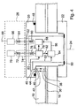
- Fig. 2 is a top front perspective view showing the optical sensor 16, in a preferred embodiment, in greater detail.
- the optical sensor 16 includes a light source 28, a detector 30, a reflective surface 32, and the conductor ribbon 18.
- the conductor ribbon 18 includes a number of generally parallel conductors laminated together for the purpose of supplying electrical power to the light source 28 and for conducting the electrical output signal of the detector 30 to the central aperture 12.
- the light source 28 and the detector 30 are a matched pair.
- the light source 28 may be a light emitting diode and the detector 30 is a photodiode.
- the central axis of the bundle of light emitted by the light source 28 is directed horizontally initially, but upon reaching the reflective surface 32 the light is redirected upward so as to strike and reflect from the surface that is being polished.
- the reflected light also is redirected by the reflective surface 32 so that the reflected light falls on the detector 30, which produces an electrical signal in relation to the intensity of the light falling on it.
- the arrangement shown in Fig. 2 was chosen to conserve the height of the sensor.
- the optical components and the end of the conductor ribbon 18 are encapsulated in the form of a thin disk 34 that is sized to fit snugly within the blind hole 14 of Fig. 1.
- baffles may be used to reduce the amount of stray light reaching the detector.
- a power conductor 36 a power conductor 36, a signal conductor 38, and one or more return or ground conductors, not shown.
- the power conductor 36 terminates adjacent the central aperture 12 of the polishing pad 10 at a power plug 40, and the signal conductor 38 likewise terminates at a signal plug 42.
- the power plug 40 makes electrical contact with the power jack 44, and the signal plug 42 makes electrical contact with the signal jack 46.
- An O-ring seal 48 prevents the liquids used in the polishing process from reaching the plugs and jacks.
- a jar lid type of seal 50 is provided in the base 22 to further insure that the electronic circuits within the hub remain uncontaminated.
- An electrical signal produced by the detector 30 and related to the optical characteristic is carried by the conductor 52 from the signal jack 46 to a signal processing circuit 54, that produces in response to the electrical signal a processed signal on the conductor 56 representing the optical characteristic.
- the processed signal on the conductor 56 is then applied to a transmitter 58.
- the transmitter 58 applies a time-varying electrical current to the primary winding 60 of a transformer that produces a varying magnetic field 62 representative of the processed signal.
- the magnetic field 62 extends upward through the top of the hub 20 and is intercepted by a secondary winding 64 of the transformer which is located on an adjacent non-rotating portion 26 of the polishing machine, or on some other non-rotating object.
- the varying magnetic field 62 induces a current in the secondary winding 64 that is applied to a receiver 66 that produces on the terminal 68 a signal representative of the optical characteristic. This signal is then available for use by external circuitry for such purposes as monitoring the progress of the polishing operation and/or determining whether the end point of the polishing process has been reached.
- a similar inductive technique may be used to transfer electrical power from the adjacent non-rotating portion 26 of the polishing machine to the rotating hub 20.
- a prime power source 70 on the non-rotating portion 26 applies an electrical current to the primary winding 72 of a transformer that produces a magnetic field 74 that extends downward through the top of the hub 20 and is intercepted by a secondary winding 76 in which the varying magnetic field induces an electrical current that is applied to a power receiver circuitry 78.
- the power receiver 78 applies electrical power on the conductor 80 to the power jack 44, from which it is conducted through the power plug 40 and the power conductor 36 to the light source 28.
- the power receiver 78 also supplies electrical power to the signal processing circuit 54 through the conductor 82, and to the transmitter 58 through the conductor 84.
- the magnetic induction technique is the best mode and preferred embodiment for transferring power into the rotating hub 20.
- the winding 60 is the same winding 76, and the winding 64 is the same winding 72.
- the superimposed power and signal components are at different frequency ranges in this embodiment and are separated by filtering.
- Figs. 5-7 show alternative embodiments in which other techniques are used to transfer signals from the rotating hub 20 to a non-rotating portion 26 of the polishing machine, and to transfer electrical power from the non-rotating portion 26 into the rotating hub 20.
- the transmitter 58 further includes a modulator 86 that applies to a light emitting diode or laser diode 88 a frequency modulated current representative of the processed signal that represents the optical characteristic.
- the light-emitting diode 88 emits light waves 90 that are focused by a lens 92 onto a photodiode detector 94.
- the detector 94 converts the light waves into an electrical signal that is demodulated in the receiver 96 to produce on the terminal 68 an electrical signal representative of the optical characteristic.
- this is the best mode and preferred technique for transferring the electrical signal from the rotating hub 20 to the non-rotating portion 26 of the polishing machine.
- the prime source of electrical power is a battery 98 that supplies power to a power distribution circuit 100 that, in turn, distributes electrical power to the power jack 44, to the signal processing circuit 54, and to the transmitter circuit 58.
- the transmitter 58 is a radio transmitter having an antenna 102 that transmits radio waves 104 through the top of the hub 20.
- the radio waves 104 are intercepted by the antenna 106 and demodulated by the receiver 103 to produce an electrical signal on the terminal 68 that is representative of the optical characteristic.
- electrical power is generated by a magneto consisting of a permanent magnet 110 located in the non-rotating portion 26 and an inductor 112 in which the magnetic field of the permanent magnet 110 induces a current as the inductor 112 rotates past the permanent magnet 110.
- the induced current is rectified and filtered by the power circuit 114 and then distributed by a power distribution circuit 116.
- the transmitter 58 further includes a power amplifier 118 that drives a loudspeaker 120 that produces sound waves 122.
- the sound waves 122 are picked up by a microphone 124 located in the non-rotating portion 26 of the polishing machine.
- the microphone 124 produces an electrical signal that is applied to the receiver 126 which, in turn, produces an electrical signal on the terminal 68 that is representative of the optical characteristic.
- electrical power is generated in the rotating hub 20 by a solar cell or solar panel 128 in response to light applied to the solar panel 128 by a light source 132 located in the non-rotating portion 26.
- the electrical output of the solar panel 128 is converted to an appropriate voltage by the converter 134, if necessary, and applied to the power distribution circuit 116.
- a polishing pad for use in a chemical mechanical polishing operation, containing an optical sensor for monitoring the condition of the surface that is being polished, during the polishing operation.
- the polishing pad including the optical system, is disposable, and is used with a non-disposable hub that contains circuitry for receiving the signal produced by the optical sensor, for processing the signal and for transmitting the signal to a non-rotating station.
- the hub also contains circuitry for supplying power to the optical sensor as well as to the other electronic circuits located in the hub.
- the signal may be transmitted from the rotating hub to the non-rotating station by radio waves, sound waves, light waves, or by magnetic induction.
- power may be supplied by including a battery in the hub or by coupling electrical power into the hub through a solar panel activated by externally applied light or by a magneto in which a stationary permanent magnet induces a current in an inductor that is mounted on the rotating hub.
- the optical sensor that is built into the polishing pad permits the progress of the polishing operation to be monitored continuously to permit the process to be terminated when a desired end point has been reached, and to avoid terminating the process too early or too late. Avoidance of these undesirable possibilities permits the polishing process to be completed more efficiently.
- the invention is applicable to the polishing or grinding of any workpiece that includes strata having different optical characteristics.
Claims (35)
- Polierscheibe (10) zum Verwenden für das Ausführen einer Polieroperation auf einer Oberfläche eines Werkstücks mit optischen Mitteln (16) innerhalb der Polierscheibe (10) zum Abtasten einer optischen Charakteristik der Oberfläche während der Polieroperation, wobei die optischen Mittel (16) Detektionsmittel (30) zum Empfangen vom Licht aufweisen, dadurch gekennzeichnet, dass die optischen Mittel (16) weiter eine Lichtquelle zum Generieren vom Licht aufweisen, um die Oberfläche des Werkstücks zu beleuchten, sodass die Detektionsmittel (30) Licht empfangen, das von der Oberfläche des Werkstücks reflektiert wird, und zum Produzieren eines elektrischen Signals, das repräsentativ für die Intensität des reflektierten Lichts ist.
- Polierscheibe (10) nach Anspruch 1, wobei die Lichtquelle (28) eine lichtemittierende Diode ist.
- Polierscheibe (10) nach Anspruch 1, wobei die Lichtquelle (28) ein Festkörper-Laser ist.
- Polierscheibe (10) nach Anspruch 1, wobei die Lichtquelle (28) so gerichtet ist, um die Oberfläche des Werkstücks zu beleuchten.
- Polierscheibe (10) nach Anspruch 1, wobei die optischen Mittel (16) weiter eine reflektierende Oberfläche (32) aufweisen, die so gerichtet ist, um das Licht, das von der Lichtquelle (28) generiert wird, auf die Oberfläche des Werkstückes zu reflektieren.
- Polierscheibe (10) nach Anspruch 1, weiter aufweisend:eine zentrale Öffnung (12); undSignalleitungsmittel (38) innerhalb der Polierscheibe (10) zum Leiten des elektrischen Signals von den optischen Mitteln (16) zu der zentralen Öffnung (12).
- Polierscheibe (10) nach Anspruch 6, wobei die Signalleitungsmittel (18) weiter eine längliche flexible Leiterplatte aufweist.
- Polierscheibe (10) nach Anspruch 6, weiter aufweisend:eine entfernbarere Nabe (20), die in der zentralen Öffnung (12) angeordnet ist und aufweist:elektrische Signalanschlussmittel (42), die mechanisch angepasst sind, um die Signalleitungsmittel (38) lösbar aufzunehmen, um dem elektrischen Signal den Eintritt in die Nabe (20) zu ermöglichen;an den elektrischen Signalanschlussmitteln (42) angeschlossene Signalverarbeitungsmittel (54) zum Empfangen des elektrischen Signals und zum Erzeugen eines verarbeiteten Signals, das die optische Charakteristik repräsentiert, in Antwort auf das elektrische Signal; undSendemittel (58), die an den Signalverarbeitungsmitteln angeschlossen sind, zum Senden des verarbeiteten Signals.
- Polierscheibe (10) nach Anspruch 8, wobei die Übertragungsmittel weiter Mittel (68) zum Emittieren von Radiowellen aufweisen, die für das verarbeitete Signal (102) repräsentativ sind.
- Polierscheibe (10) nach Anspruch 8, wobei die Sendemittel weiter Mittel zum Emittieren von Schallwellen aufweisen, die das verarbeitete Signal (118, 120) repräsentieren.
- Polierscheibe (10) nach Anspruch 8, wobei die Sendemittel weiter Mittel zum Emittieren von Lichtwellen aufweisen, die das verarbeitete Signal (86, 88) repräsentieren.
- Polierscheibe (10) nach Anspruch 8, wobei die Sendemittel weiter Mittel zum Erzeugen eines variablen Magnetfelds aufweisen, das das verarbeitete Signal (62) repräsentiert.
- Polierscheibe (10) nach Anspruch 1, weiter aufweisend:eine zentrale Öffnung (12);einen Energieleiter (18), der sich von der zentralen Öffnung (12) zu den optischen Mitteln (16) erstreckt, zum Liefern von elektrischer Energie an die optischen Mittel (16); undeine entfernbare Nabe (20), die in der zentralen Öffnung (12) der Polierscheibe (10) angeordnet ist, wobei die entfernbare Nabe (20) aufweist:Energieempfangsmittel (76, 78) zum Erzeugen von elektrischer Energie in Antwort auf extern angelegte Energie; undAnschlussmittel für elektrische Energie (44), die mechanisch angepasst sind, um lösbar den Energieleiter (18) aufzunehmen, zum Anlegen der elektrischen Energie an den Energieleiter (18), die mittels der Energieempfangsmittel erzeugt wird.
- Polierscheibe (10) nach Anspruch 13, wobei die Energieempfangsmittel eine Solarzelle (128) aufweisen, die elektrische Energie in Antwort auf extern angelegtes Licht erzeugt.
- Polierscheibe (10) nach Anspruch 13, wobei die Energieempfangsmittel (78) einen Induktor (112) aufweisen, der elektrische Energie in Antwort auf Veränderungen eines angelegten magnetischen Felds erzeugt, das durch den Induktor passiert.
- Polierscheibe (10) nach Anspruch 1, weiter aufweisend:eine zentrale Öffnung (12);einen Energieleiter (18), der sich von der zentralen Öffnung (12) der Polierscheibe (10) zu dem optischen Mitteln (16) erstreckt, zum Liefern von elektrischer Energie an die optischen Mittel (16);eine entfernbare Nabe (20), die in der zentralen Öffnung (12) der Polierscheibe (10) angeordnet ist und aufweist:eine Batterie zum Erzeugen von elektrischer Energie; undAnschlussmittel für elektrische Energie, die mechanisch angepasst sind, um entfernbar den Energieleiter (18) aufzunehmen, zum Anlegen der elektrischen Energie an den Energieleiter (18), die mittels der Batterie erzeugt wird.
- System zum Polieren von Wafern und zum Bestimmen des Endpunkts von bestimmten Poliervorgängen aufweisend eine Polierscheibe (10) nach einem der Ansprüche 1 bis 16, die an einer Platte gesichert wird, um damit drehbar zu sein;
ein induktives Kopplungssystem, das an den optischen Mitteln (16) angeschlossen ist, um induktiv Signale von der Scheibe während der Drehung zu einem ortsfesten Empfänger zu übertragen, wobei das induktive Kopplungssystem eine erste Transformatorwicklung (60), die so an der Scheibe (10) gesichert ist, dass sie mit der Scheibe rotiert, und eine zweite Transformatorwicklung (64) innerhalb des ortsfesten Empfängers und ein Mittel (54) aufweist, um das elektrische Ausgabesignal von dem optischen Sensor (16) zu der ersten Transformatorwicklung (60) zu übertragen. - System nach Anspruch 17, wobei das induktive Kopplungssystem weiter Mittel zum Umwandeln der Ausgabe der optischen Mittel (16) in eine zeitvariierende elektrische Eingabe an die erste Transformatorwicklung aufweist.
- System nach Anspruch 17, wobei die optischen Mittel (16) gegen das Zentrum in der Polierscheibe (10) versetzt angeordnet sind und wobei die erste Transformatorwicklung (60) in der Nähe des Zentrums der Scheibe (10) gesichert ist und der ortsfeste Empfänger (26) derart in Beziehung zu der ersten Transformatorwicklung angeordnet ist, dass die zweite Transformatorwicklung (64) in betriebsfähiger Umgebung der ersten Transformatorwicklung (60) gehalten ist.
- System nach Anspruch 18, weiter aufweisend:eine Nabe (20), die im Zentrum der Polierscheibe (10) angeordnet ist, wobei die Nabe (20) die erste Transformatorwicklung (60) aufnimmt, wobei der ortsfeste Empfänger (26) über der Nabe (20) aufgehängt ist, sodass die zweite Transformatorwicklung (64) in betriebsfähiger Umgebung der ersten Transformatorwicklung (60) gehalten ist.
- Polierscheibe (10) nach Anspruch 1, weiter aufweisend:Mittel (54) zum Verarbeiten des elektrischen Signals, das dem reflektierten Licht entspricht, und zum Erzeugen eines zeitvariierenden elektrischen Signals, das dem reflektierten Licht entspricht;einen Sender (58) zum Erzeugen eines zeitvariierenden elektrischen Signals, das dem verarbeiteten Signal entspricht; und eine erste Transformatorwicklung (60), die angepasst ist, um das zeitveränderliche elektrische Ausgabesignal des Senders zu empfangen.
- Polierscheibe (10) nach Anspruch 21, wobei:der Detektor (30) eine Photodiode aufweist, die zu der Menge des detektierten reflektierten Lichts proportionalen Strom erzeugt, und wobei das Mittel zum Verarbeiten des elektrischen Signals und zum Erzeugen eines zeitvariierenden elektrischen Signals einen Signalprozessor (54), der angepasst ist, um ein verarbeitetes elektrisches Signal zu erzeugen, das dem Ausgabestrom von der Photodiode entspricht, und einen Sender aufweist, der angepasst ist, um einen zeitvariierenden Strom zu erzeugen, der dem verarbeiteten Signal entspricht.
- Polierscheibe (10) nach Anspruch 21, wobei die erste Transformatorwicklung (60) nahe am Zentrum der Scheibe (10) angeordnet und an der Scheibe gesichert ist, sodass sie sich mit der Scheibe dreht, wenn sich die Scheibe dreht.
- Polierscheibe (10) nach einem der Ansprüche 21 bis 23, wobei das Mittel zum Verarbeiten des elektrischen Signals, das dem reflektierten Licht entspricht und das das elektrische zeitabhängige Signal erzeugt, und die erste Transformatorwicklung (60) innerhalb der Nabe (20) angeordnet sind, der an dem Zentrum des Polierscheibe (10) gesichert ist.
- Polierscheibe (10) nach Anspruch 21 oder 22, weiter eine zweite Energietransformatorwicklung (76), die an der Polierscheibe (10) gesichert ist, und Mittel zum Liefern von Energie an die Lichtquelle (28) von der Ausgabe der zweiten Energietransformatorwicklung (76) aufweisend.
- System zum Polieren von Wafern und zum Bestimmen des Endpunkts von bestimmten Poliervorgängen, aufweisend:eine Polierscheibe (10) nach einem der Ansprüche 1 bis 16, die an einer Platte gesichert wird, um damit drehbar zu sein; undein optisches Kopplungssystem, das an den optischen Mitteln (16) angeschlossen ist, um optisch Signale von der Scheibe während der Drehung zu einem ortsfesten Empfänger (26) zu übertragen, wobei das optische Kopplungssystem eine LED (88), die an der Scheibe (10) gesichert ist, sodass sie mit der Scheibe rotiert, und einen Detektor (94), der das Ausgabelichtsignal von der LED (88) in ein elektrisches Signal umwandelt, das für die optische Charakteristik der Waferoberfläche repräsentativ ist, wobei der Detektor (94) innerhalb des ortsfesten Empfängers (26) angeordnet ist, undein Mittel aufweist, um das elektrische Ausgabesignal von dem optischen Sensor (16) zu der LED zu übertragen.
- System nach Anspruch 26, wobei das optische Kopplungssystem weiter Mittel (54) zum Umwandeln der Ausgabe der optischen Mittel (16) in eine frequenzmodulierte elektrische Eingabe an die LED aufweist.
- System nach Anspruch 26, wobei die optischen Mittel (16) gegen das Zentrum in dem Polierscheibe (10) versetzt angeordnet sind und die LED (88) in der Nähe des Zentrums der Scheibe gesichert ist und der ortsfeste Empfänger so in Beziehung zu der LED (88) angeordnet ist, dass der Detektor (30) in betriebsfähiger Umgebung der LED (88) festgehalten wird.
- System nach Anspruch 26, weiter aufweisend:eine Nabe (20), die im Zentrum der Polierscheibe (10) angeordnet ist, wobei die Nabe (20) die LED (88) aufnimmt, wobei der ortsfeste Empfänger (26) über der Nabe (20) aufgehängt ist, sodass der Detektor (94) in betriebsfähiger Umgebung der LED (88) gehalten ist.
- Polierscheibe (10) nach Anspruch 1, weiter aufweisend Mittel (54, 58, 86) zum Verarbeiten des elektrischen Signals, das dem reflektierten Licht entspricht, und zum Produzieren eines frequenzmodulierten elektrischen Signals, das dem reflektierten Licht entspricht; und
eine LED (88), die angepasst ist, um das frequenzmodulierte elektrische Ausgabesignal des Senders zu empfangen und um eine entsprechende Lichtausgabe zu erzeugen. - Polierscheibe (10) nach Anspruch 30, wobei:das Mittel (54) zum Verarbeiten des elektrischen Signals undzum Erzeugen eines frequenzmodulierten elektrischen Signals einen Signalprozessor, der angepasst ist, um ein verarbeitetes elektrisches Signal zu produzieren, das zu dem Ausgabestrom an der Photodiode korrespondiert, und einen Sender aufweist, der angepasst ist, um einen frequenzmodulierten Strom zu erzeugen, der dem verarbeiteten Signal entspricht.
- Polierscheibe (10) nach Anspruch 30 oder 31, wobei die LED (88) in der Nähe des Zentrums der Scheibe angeordnet ist und an der Scheibe gesichert ist, sodass sie sich mit der Scheibe dreht, wenn sich die Scheibe dreht.
- Polierscheibe (10) nach einem der Ansprüche 30 bis 32, wobei das Mittel zum Verarbeiten des elektrischen Signals, das dem reflektierten Licht entspricht, und zum Erzeugen des frequenzmodulierten elektrischen Signals und die LED innerhalb einer Nabe (20) angeordnet sind, die im Zentrum der Polierscheibe (10) befestigt ist.
- Polierscheibe (10) nach einem der Ansprüche 30 bis 33, weiter eine zweite Energietransformatorwicklung (76), die an der Polierscheibe (10) befestigt ist, und Mittel (78) zum Bereitstellen von Energie an das Mittel zum Führen des Lichtes von der Ausgabe der zweiten Energietransformatorwicklung (76) aufweisend.
- Polierscheibe (10) nach Anspruch 1, weiter aufweisend:Mittel (54) zum Verarbeiten des elektrischen Signals entsprechend dem reflektierten Licht und zum Erzeugen eines entsprechenden verarbeiteten Signals;einen Sender (58) zum Erzeugen eines frequenzmodulierten elektrischen Signals, das dem verarbeiteten Signal entspricht; und eine LED (88), die angepasst ist, um das frequenzmodulierte elektrische Ausgabesignal des Senders (58) zu empfangen und ein zeitvariierendes optisches Signal zu erzeugen.
Applications Claiming Priority (3)
| Application Number | Priority Date | Filing Date | Title |
|---|---|---|---|
| US590470 | 2000-06-09 | ||
| US09/590,470 US6485354B1 (en) | 2000-06-09 | 2000-06-09 | Polishing pad with built-in optical sensor |
| PCT/US2000/018399 WO2001096062A1 (en) | 2000-06-09 | 2000-07-03 | Polishing pad with built-in optical sensor |
Publications (3)
| Publication Number | Publication Date |
|---|---|
| EP1296800A1 EP1296800A1 (de) | 2003-04-02 |
| EP1296800A4 EP1296800A4 (de) | 2003-08-06 |
| EP1296800B1 true EP1296800B1 (de) | 2005-06-08 |
Family
ID=24362394
Family Applications (1)
| Application Number | Title | Priority Date | Filing Date |
|---|---|---|---|
| EP00947036A Expired - Lifetime EP1296800B1 (de) | 2000-06-09 | 2000-07-03 | Polierkissen mit integriertem optischen sensor |
Country Status (11)
| Country | Link |
|---|---|
| US (6) | US6485354B1 (de) |
| EP (1) | EP1296800B1 (de) |
| JP (1) | JP5031170B2 (de) |
| KR (1) | KR100766139B1 (de) |
| CN (2) | CN101125414A (de) |
| AT (1) | ATE297291T1 (de) |
| AU (1) | AU2000260706A1 (de) |
| DE (1) | DE60020746T2 (de) |
| SG (1) | SG133404A1 (de) |
| TW (1) | TW553804B (de) |
| WO (1) | WO2001096062A1 (de) |
Families Citing this family (39)
| Publication number | Priority date | Publication date | Assignee | Title |
|---|---|---|---|---|
| US5893796A (en) * | 1995-03-28 | 1999-04-13 | Applied Materials, Inc. | Forming a transparent window in a polishing pad for a chemical mechanical polishing apparatus |
| US6876454B1 (en) | 1995-03-28 | 2005-04-05 | Applied Materials, Inc. | Apparatus and method for in-situ endpoint detection for chemical mechanical polishing operations |
| DE69635816T2 (de) * | 1995-03-28 | 2006-10-12 | Applied Materials, Inc., Santa Clara | Verfahren zum Herstellen einer Vorrichtung zur In-Situ-Kontrolle und Bestimmung des Endes von chemisch-mechanischen Planiervorgängen |
| US6726528B2 (en) * | 2002-05-14 | 2004-04-27 | Strasbaugh | Polishing pad with optical sensor |
| US6976901B1 (en) * | 1999-10-27 | 2005-12-20 | Strasbaugh | In situ feature height measurement |
| US6485354B1 (en) * | 2000-06-09 | 2002-11-26 | Strasbaugh | Polishing pad with built-in optical sensor |
| US20020137431A1 (en) * | 2001-03-23 | 2002-09-26 | Labunsky Michael A. | Methods and apparatus for polishing and planarization |
| US6780085B2 (en) * | 2001-11-23 | 2004-08-24 | Stephan H. Wolf | Fiber optical sensor embedded into the polishing pad for in-situ, real-time, monitoring of thin films during the chemical mechanical planarization process |
| US7074110B1 (en) | 2001-11-23 | 2006-07-11 | Stephan H Wolf | Optical coupler hub for chemical-mechanical-planarization polishing pads with an integrated optical waveguide |
| US6878039B2 (en) * | 2002-01-28 | 2005-04-12 | Speedfam-Ipec Corporation | Polishing pad window for a chemical-mechanical polishing tool |
| US20030181136A1 (en) * | 2002-03-22 | 2003-09-25 | Billett Bruce H. | CMP pad platen with viewport |
| US7040957B2 (en) * | 2002-08-14 | 2006-05-09 | Novellus Systems Inc. | Platen and manifold for polishing workpieces |
| US7727049B2 (en) * | 2003-10-31 | 2010-06-01 | Applied Materials, Inc. | Friction sensor for polishing system |
| JP4764825B2 (ja) * | 2003-10-31 | 2011-09-07 | アプライド マテリアルズ インコーポレイテッド | 研磨終点検知システム及び摩擦センサを使用する方法 |
| US7235154B2 (en) * | 2004-01-08 | 2007-06-26 | Strasbaugh | Devices and methods for optical endpoint detection during semiconductor wafer polishing |
| US7091053B2 (en) * | 2004-03-26 | 2006-08-15 | Taiwan Semiconductor Manufacturing Company | In-line wafer surface mapping |
| US20050277841A1 (en) * | 2004-06-10 | 2005-12-15 | Adnan Shennib | Disposable fetal monitor patch |
| US20060030781A1 (en) * | 2004-08-05 | 2006-02-09 | Adnan Shennib | Emergency heart sensor patch |
| US20060030782A1 (en) * | 2004-08-05 | 2006-02-09 | Adnan Shennib | Heart disease detection patch |
| WO2006089291A1 (en) * | 2005-02-18 | 2006-08-24 | Neopad Technologies Corporation | Use of phosphorescent materials for two-dimensional wafer mapping in a chemical mechanical polishing |
| US7169016B2 (en) * | 2005-05-10 | 2007-01-30 | Nikon Corporation | Chemical mechanical polishing end point detection apparatus and method |
| US8688189B2 (en) * | 2005-05-17 | 2014-04-01 | Adnan Shennib | Programmable ECG sensor patch |
| US20070255184A1 (en) * | 2006-02-10 | 2007-11-01 | Adnan Shennib | Disposable labor detection patch |
| US20070191728A1 (en) * | 2006-02-10 | 2007-08-16 | Adnan Shennib | Intrapartum monitor patch |
| JP4814677B2 (ja) * | 2006-03-31 | 2011-11-16 | 株式会社荏原製作所 | 基板保持装置および研磨装置 |
| US7887392B2 (en) * | 2007-06-06 | 2011-02-15 | Novellus Systems, Inc. | Platen assembly and work piece carrier head employing flexible circuit sensor |
| TWM347669U (en) * | 2008-06-19 | 2008-12-21 | Bestac Advanced Material Co Ltd | Polishing pad and polishing device |
| US9017140B2 (en) | 2010-01-13 | 2015-04-28 | Nexplanar Corporation | CMP pad with local area transparency |
| US9156124B2 (en) | 2010-07-08 | 2015-10-13 | Nexplanar Corporation | Soft polishing pad for polishing a semiconductor substrate |
| CN102371540B (zh) * | 2010-08-19 | 2013-12-04 | 中芯国际集成电路制造(上海)有限公司 | 抛光垫清理器 |
| US20140020829A1 (en) * | 2012-07-18 | 2014-01-23 | Applied Materials, Inc. | Sensors in Carrier Head of a CMP System |
| US9347634B2 (en) * | 2013-02-25 | 2016-05-24 | Ford Global Technologies, Llc | Illuminating floor mat with wireless power transfer |
| US20140329439A1 (en) * | 2013-05-01 | 2014-11-06 | Applied Materials, Inc. | Apparatus and methods for acoustical monitoring and control of through-silicon-via reveal processing |
| US9347822B2 (en) * | 2014-05-07 | 2016-05-24 | Tyco Electronics Corporation | Photocell receptacle having variably positionable cap and base |
| CN104057395B (zh) * | 2014-07-17 | 2016-04-13 | 成都精密光学工程研究中心 | 抛光模面形监测装置 |
| US10034109B2 (en) * | 2015-04-09 | 2018-07-24 | Audera Acoustics Inc. | Acoustic transducer systems with position sensing |
| US10160089B2 (en) * | 2015-10-01 | 2018-12-25 | Ebara Corporation | Polishing apparatus |
| CN108630561B (zh) * | 2017-03-15 | 2021-10-15 | 北京北方华创微电子装备有限公司 | 基片表面的检测装置和检测方法、传片腔室 |
| US11660722B2 (en) | 2018-08-31 | 2023-05-30 | Applied Materials, Inc. | Polishing system with capacitive shear sensor |
Family Cites Families (28)
| Publication number | Priority date | Publication date | Assignee | Title |
|---|---|---|---|---|
| US583447A (en) * | 1897-06-01 | Stove or furnace | ||
| US4793895A (en) * | 1988-01-25 | 1988-12-27 | Ibm Corporation | In situ conductivity monitoring technique for chemical/mechanical planarization endpoint detection |
| US4972089A (en) | 1989-04-03 | 1990-11-20 | Motorola Inc. | Single package electro-optic transmitter-receiver |
| US5132617A (en) * | 1990-05-16 | 1992-07-21 | International Business Machines Corp. | Method of measuring changes in impedance of a variable impedance load by disposing an impedance connected coil within the air gap of a magnetic core |
| US5081793A (en) * | 1990-06-07 | 1992-01-21 | Mauro Gerald D | Wood clad window assembly and associated method |
| US5081796A (en) | 1990-08-06 | 1992-01-21 | Micron Technology, Inc. | Method and apparatus for mechanical planarization and endpoint detection of a semiconductor wafer |
| US6614529B1 (en) | 1992-12-28 | 2003-09-02 | Applied Materials, Inc. | In-situ real-time monitoring technique and apparatus for endpoint detection of thin films during chemical/mechanical polishing planarization |
| US5700180A (en) * | 1993-08-25 | 1997-12-23 | Micron Technology, Inc. | System for real-time control of semiconductor wafer polishing |
| US5964643A (en) | 1995-03-28 | 1999-10-12 | Applied Materials, Inc. | Apparatus and method for in-situ monitoring of chemical mechanical polishing operations |
| US5893796A (en) | 1995-03-28 | 1999-04-13 | Applied Materials, Inc. | Forming a transparent window in a polishing pad for a chemical mechanical polishing apparatus |
| DE69635816T2 (de) * | 1995-03-28 | 2006-10-12 | Applied Materials, Inc., Santa Clara | Verfahren zum Herstellen einer Vorrichtung zur In-Situ-Kontrolle und Bestimmung des Endes von chemisch-mechanischen Planiervorgängen |
| JP3601910B2 (ja) * | 1995-07-20 | 2004-12-15 | 株式会社荏原製作所 | ポリッシング装置及び方法 |
| US5838447A (en) | 1995-07-20 | 1998-11-17 | Ebara Corporation | Polishing apparatus including thickness or flatness detector |
| JPH0929620A (ja) * | 1995-07-20 | 1997-02-04 | Ebara Corp | ポリッシング装置 |
| US6010538A (en) * | 1996-01-11 | 2000-01-04 | Luxtron Corporation | In situ technique for monitoring and controlling a process of chemical-mechanical-polishing via a radiative communication link |
| US5663637A (en) * | 1996-03-19 | 1997-09-02 | International Business Machines Corporation | Rotary signal coupling for chemical mechanical polishing endpoint detection with a westech tool |
| US6012697A (en) * | 1996-04-12 | 2000-01-11 | Nikon Corporation | Stage and supporting mechanism for supporting movable mirror on stage |
| JP3672685B2 (ja) | 1996-11-29 | 2005-07-20 | 松下電器産業株式会社 | 研磨方法及び研磨装置 |
| JPH10214804A (ja) * | 1997-01-28 | 1998-08-11 | Olympus Optical Co Ltd | 機械化学研磨装置用の平坦化過程モニター装置 |
| JP3795185B2 (ja) * | 1997-06-04 | 2006-07-12 | 株式会社荏原製作所 | ポリッシング装置 |
| JPH1133914A (ja) * | 1997-07-22 | 1999-02-09 | Koei Sangyo Kk | ラップ盤の研磨液供給装置 |
| US5913713A (en) | 1997-07-31 | 1999-06-22 | International Business Machines Corporation | CMP polishing pad backside modifications for advantageous polishing results |
| US6007408A (en) * | 1997-08-21 | 1999-12-28 | Micron Technology, Inc. | Method and apparatus for endpointing mechanical and chemical-mechanical polishing of substrates |
| JP3183259B2 (ja) * | 1998-06-03 | 2001-07-09 | 日本電気株式会社 | 半導体ウェハ研磨状態モニタリング装置及び研磨終了点検出方法 |
| US6106662A (en) * | 1998-06-08 | 2000-08-22 | Speedfam-Ipec Corporation | Method and apparatus for endpoint detection for chemical mechanical polishing |
| US6190234B1 (en) * | 1999-01-25 | 2001-02-20 | Applied Materials, Inc. | Endpoint detection with light beams of different wavelengths |
| US6146242A (en) * | 1999-06-11 | 2000-11-14 | Strasbaugh, Inc. | Optical view port for chemical mechanical planarization endpoint detection |
| US6485354B1 (en) * | 2000-06-09 | 2002-11-26 | Strasbaugh | Polishing pad with built-in optical sensor |
-
2000
- 2000-06-09 US US09/590,470 patent/US6485354B1/en not_active Expired - Lifetime
- 2000-07-03 AU AU2000260706A patent/AU2000260706A1/en not_active Abandoned
- 2000-07-03 SG SG200407621-2A patent/SG133404A1/en unknown
- 2000-07-03 CN CNA2007101423465A patent/CN101125414A/zh active Pending
- 2000-07-03 JP JP2002510230A patent/JP5031170B2/ja not_active Expired - Fee Related
- 2000-07-03 EP EP00947036A patent/EP1296800B1/de not_active Expired - Lifetime
- 2000-07-03 KR KR1020027016714A patent/KR100766139B1/ko not_active IP Right Cessation
- 2000-07-03 CN CNB008198004A patent/CN100340372C/zh not_active Expired - Fee Related
- 2000-07-03 DE DE60020746T patent/DE60020746T2/de not_active Expired - Lifetime
- 2000-07-03 AT AT00947036T patent/ATE297291T1/de not_active IP Right Cessation
- 2000-07-03 WO PCT/US2000/018399 patent/WO2001096062A1/en active IP Right Grant
- 2000-10-04 TW TW089120611A patent/TW553804B/zh not_active IP Right Cessation
-
2002
- 2002-11-25 US US10/303,621 patent/US6695681B2/en not_active Expired - Lifetime
-
2004
- 2004-02-23 US US10/785,393 patent/US7052366B2/en not_active Expired - Lifetime
-
2006
- 2006-05-30 US US11/443,788 patent/US7195541B2/en not_active Expired - Lifetime
-
2007
- 2007-03-27 US US11/729,303 patent/US20090061734A1/en not_active Abandoned
-
2010
- 2010-02-12 US US12/705,091 patent/US7918712B2/en not_active Expired - Lifetime
Also Published As
| Publication number | Publication date |
|---|---|
| KR100766139B1 (ko) | 2007-10-10 |
| CN100340372C (zh) | 2007-10-03 |
| US6695681B2 (en) | 2004-02-24 |
| US7052366B2 (en) | 2006-05-30 |
| SG133404A1 (en) | 2007-07-30 |
| US7918712B2 (en) | 2011-04-05 |
| ATE297291T1 (de) | 2005-06-15 |
| US20060217038A1 (en) | 2006-09-28 |
| TW553804B (en) | 2003-09-21 |
| US20040229545A1 (en) | 2004-11-18 |
| KR20030022142A (ko) | 2003-03-15 |
| US20100144244A1 (en) | 2010-06-10 |
| JP5031170B2 (ja) | 2012-09-19 |
| CN101125414A (zh) | 2008-02-20 |
| DE60020746T2 (de) | 2006-03-16 |
| EP1296800A4 (de) | 2003-08-06 |
| JP2004503925A (ja) | 2004-02-05 |
| AU2000260706A1 (en) | 2001-12-24 |
| EP1296800A1 (de) | 2003-04-02 |
| US6485354B1 (en) | 2002-11-26 |
| US20090061734A1 (en) | 2009-03-05 |
| US20030109196A1 (en) | 2003-06-12 |
| CN1454131A (zh) | 2003-11-05 |
| US7195541B2 (en) | 2007-03-27 |
| WO2001096062A1 (en) | 2001-12-20 |
| DE60020746D1 (de) | 2005-07-14 |
Similar Documents
| Publication | Publication Date | Title |
|---|---|---|
| EP1296800B1 (de) | Polierkissen mit integriertem optischen sensor | |
| US7083497B2 (en) | Polishing pad with built-in optical sensor | |
| US20070235133A1 (en) | Devices and methods for measuring wafer characteristics during semiconductor wafer polishing | |
| US7549909B2 (en) | Methods for optical endpoint detection during semiconductor wafer polishing | |
| US6696005B2 (en) | Method for making a polishing pad with built-in optical sensor |
Legal Events
| Date | Code | Title | Description |
|---|---|---|---|
| PUAI | Public reference made under article 153(3) epc to a published international application that has entered the european phase |
Free format text: ORIGINAL CODE: 0009012 |
|
| 17P | Request for examination filed |
Effective date: 20030109 |
|
| AK | Designated contracting states |
Designated state(s): AT BE CH CY DE DK ES FI FR GB GR IE IT LI LU MC NL PT SE Kind code of ref document: A1 Designated state(s): AT BE CH CY DE DK ES FI FR GB GR IE IT LI LU MC NL PT SE |
|
| AX | Request for extension of the european patent |
Extension state: AL LT LV MK RO SI |
|
| A4 | Supplementary search report drawn up and despatched |
Effective date: 20030623 |
|
| RIC1 | Information provided on ipc code assigned before grant |
Ipc: 7B 24B 37/04 A Ipc: 7B 24B 49/04 B Ipc: 7B 24B 49/12 B Ipc: 7B 24D 7/12 B |
|
| 17Q | First examination report despatched |
Effective date: 20031110 |
|
| GRAP | Despatch of communication of intention to grant a patent |
Free format text: ORIGINAL CODE: EPIDOSNIGR1 |
|
| GRAS | Grant fee paid |
Free format text: ORIGINAL CODE: EPIDOSNIGR3 |
|
| GRAA | (expected) grant |
Free format text: ORIGINAL CODE: 0009210 |
|
| AK | Designated contracting states |
Kind code of ref document: B1 Designated state(s): AT BE CH CY DE DK ES FI FR GB GR IE IT LI LU MC NL PT SE |
|
| PG25 | Lapsed in a contracting state [announced via postgrant information from national office to epo] |
Ref country code: BE Free format text: LAPSE BECAUSE OF FAILURE TO SUBMIT A TRANSLATION OF THE DESCRIPTION OR TO PAY THE FEE WITHIN THE PRESCRIBED TIME-LIMIT Effective date: 20050608 Ref country code: CH Free format text: LAPSE BECAUSE OF FAILURE TO SUBMIT A TRANSLATION OF THE DESCRIPTION OR TO PAY THE FEE WITHIN THE PRESCRIBED TIME-LIMIT Effective date: 20050608 Ref country code: NL Free format text: LAPSE BECAUSE OF FAILURE TO SUBMIT A TRANSLATION OF THE DESCRIPTION OR TO PAY THE FEE WITHIN THE PRESCRIBED TIME-LIMIT Effective date: 20050608 Ref country code: AT Free format text: LAPSE BECAUSE OF FAILURE TO SUBMIT A TRANSLATION OF THE DESCRIPTION OR TO PAY THE FEE WITHIN THE PRESCRIBED TIME-LIMIT Effective date: 20050608 Ref country code: LI Free format text: LAPSE BECAUSE OF FAILURE TO SUBMIT A TRANSLATION OF THE DESCRIPTION OR TO PAY THE FEE WITHIN THE PRESCRIBED TIME-LIMIT Effective date: 20050608 Ref country code: ES Free format text: LAPSE BECAUSE OF FAILURE TO SUBMIT A TRANSLATION OF THE DESCRIPTION OR TO PAY THE FEE WITHIN THE PRESCRIBED TIME-LIMIT Effective date: 20050608 Ref country code: FI Free format text: LAPSE BECAUSE OF FAILURE TO SUBMIT A TRANSLATION OF THE DESCRIPTION OR TO PAY THE FEE WITHIN THE PRESCRIBED TIME-LIMIT Effective date: 20050608 |
|
| REG | Reference to a national code |
Ref country code: GB Ref legal event code: FG4D |
|
| REG | Reference to a national code |
Ref country code: CH Ref legal event code: EP |
|
| PG25 | Lapsed in a contracting state [announced via postgrant information from national office to epo] |
Ref country code: LU Free format text: LAPSE BECAUSE OF NON-PAYMENT OF DUE FEES Effective date: 20050703 Ref country code: CY Free format text: LAPSE BECAUSE OF FAILURE TO SUBMIT A TRANSLATION OF THE DESCRIPTION OR TO PAY THE FEE WITHIN THE PRESCRIBED TIME-LIMIT Effective date: 20050703 |
|
| PG25 | Lapsed in a contracting state [announced via postgrant information from national office to epo] |
Ref country code: IE Free format text: LAPSE BECAUSE OF NON-PAYMENT OF DUE FEES Effective date: 20050704 |
|
| REF | Corresponds to: |
Ref document number: 60020746 Country of ref document: DE Date of ref document: 20050714 Kind code of ref document: P |
|
| REG | Reference to a national code |
Ref country code: IE Ref legal event code: FG4D |
|
| PG25 | Lapsed in a contracting state [announced via postgrant information from national office to epo] |
Ref country code: MC Free format text: LAPSE BECAUSE OF NON-PAYMENT OF DUE FEES Effective date: 20050731 |
|
| PG25 | Lapsed in a contracting state [announced via postgrant information from national office to epo] |
Ref country code: DK Free format text: LAPSE BECAUSE OF FAILURE TO SUBMIT A TRANSLATION OF THE DESCRIPTION OR TO PAY THE FEE WITHIN THE PRESCRIBED TIME-LIMIT Effective date: 20050908 Ref country code: GR Free format text: LAPSE BECAUSE OF FAILURE TO SUBMIT A TRANSLATION OF THE DESCRIPTION OR TO PAY THE FEE WITHIN THE PRESCRIBED TIME-LIMIT Effective date: 20050908 Ref country code: SE Free format text: LAPSE BECAUSE OF FAILURE TO SUBMIT A TRANSLATION OF THE DESCRIPTION OR TO PAY THE FEE WITHIN THE PRESCRIBED TIME-LIMIT Effective date: 20050908 |
|
| PG25 | Lapsed in a contracting state [announced via postgrant information from national office to epo] |
Ref country code: PT Free format text: LAPSE BECAUSE OF FAILURE TO SUBMIT A TRANSLATION OF THE DESCRIPTION OR TO PAY THE FEE WITHIN THE PRESCRIBED TIME-LIMIT Effective date: 20051114 |
|
| NLV1 | Nl: lapsed or annulled due to failure to fulfill the requirements of art. 29p and 29m of the patents act | ||
| REG | Reference to a national code |
Ref country code: CH Ref legal event code: PL |
|
| ET | Fr: translation filed | ||
| PLBE | No opposition filed within time limit |
Free format text: ORIGINAL CODE: 0009261 |
|
| STAA | Information on the status of an ep patent application or granted ep patent |
Free format text: STATUS: NO OPPOSITION FILED WITHIN TIME LIMIT |
|
| REG | Reference to a national code |
Ref country code: IE Ref legal event code: MM4A |
|
| 26N | No opposition filed |
Effective date: 20060309 |
|
| PGFP | Annual fee paid to national office [announced via postgrant information from national office to epo] |
Ref country code: GB Payment date: 20130624 Year of fee payment: 14 |
|
| PGFP | Annual fee paid to national office [announced via postgrant information from national office to epo] |
Ref country code: DE Payment date: 20130731 Year of fee payment: 14 |
|
| PGFP | Annual fee paid to national office [announced via postgrant information from national office to epo] |
Ref country code: FR Payment date: 20130712 Year of fee payment: 14 |
|
| PGFP | Annual fee paid to national office [announced via postgrant information from national office to epo] |
Ref country code: IT Payment date: 20130716 Year of fee payment: 14 |
|
| REG | Reference to a national code |
Ref country code: DE Ref legal event code: R119 Ref document number: 60020746 Country of ref document: DE |
|
| GBPC | Gb: european patent ceased through non-payment of renewal fee |
Effective date: 20140703 |
|
| REG | Reference to a national code |
Ref country code: FR Ref legal event code: ST Effective date: 20150331 |
|
| PG25 | Lapsed in a contracting state [announced via postgrant information from national office to epo] |
Ref country code: DE Free format text: LAPSE BECAUSE OF NON-PAYMENT OF DUE FEES Effective date: 20150203 Ref country code: IT Free format text: LAPSE BECAUSE OF NON-PAYMENT OF DUE FEES Effective date: 20140703 |
|
| REG | Reference to a national code |
Ref country code: DE Ref legal event code: R119 Ref document number: 60020746 Country of ref document: DE Effective date: 20150203 |
|
| PG25 | Lapsed in a contracting state [announced via postgrant information from national office to epo] |
Ref country code: FR Free format text: LAPSE BECAUSE OF NON-PAYMENT OF DUE FEES Effective date: 20140731 Ref country code: GB Free format text: LAPSE BECAUSE OF NON-PAYMENT OF DUE FEES Effective date: 20140703 |