EP1294055A2 - Steckverbinderanordnung mit einer Federbuchse und einem Doppelkontakt mit einem Paar von versetzten Kontaktelementen - Google Patents
Steckverbinderanordnung mit einer Federbuchse und einem Doppelkontakt mit einem Paar von versetzten Kontaktelementen Download PDFInfo
- Publication number
- EP1294055A2 EP1294055A2 EP02012381A EP02012381A EP1294055A2 EP 1294055 A2 EP1294055 A2 EP 1294055A2 EP 02012381 A EP02012381 A EP 02012381A EP 02012381 A EP02012381 A EP 02012381A EP 1294055 A2 EP1294055 A2 EP 1294055A2
- Authority
- EP
- European Patent Office
- Prior art keywords
- contact
- tab
- conductor
- bus bar
- electrical
- Prior art date
- Legal status (The legal status is an assumption and is not a legal conclusion. Google has not performed a legal analysis and makes no representation as to the accuracy of the status listed.)
- Granted
Links
Images


Classifications
-
- H—ELECTRICITY
- H01—ELECTRIC ELEMENTS
- H01R—ELECTRICALLY-CONDUCTIVE CONNECTIONS; STRUCTURAL ASSOCIATIONS OF A PLURALITY OF MUTUALLY-INSULATED ELECTRICAL CONNECTING ELEMENTS; COUPLING DEVICES; CURRENT COLLECTORS
- H01R13/00—Details of coupling devices of the kinds covered by groups H01R12/70 or H01R24/00 - H01R33/00
- H01R13/02—Contact members
- H01R13/10—Sockets for co-operation with pins or blades
- H01R13/11—Resilient sockets
Definitions
- the present invention relates, in particular but not exclusively, to the field of bus bar assemblies. More specifically, the present invention relates to a device for connecting an electrical contact to a conductor provided with a tab, an electrical contact comprising a first pair of spaced apart contact members and a second pair of spaced apart contact tails, an electrical connector comprising an insulating housing and the electrical contact, a connector assembly comprising the connecting device and electrical contact, and a bus bar system with a backplane printed circuit board having at least one opening.
- An object of the present invention is to fulfil this need of the industry.
- a device for connecting an electrical contact to a conductor provided with a tab comprising a socket member structured to receive the tab of the conductor and the electrical contact in order to interconnect these tab and contact, and a tubular member having a first section in which the socket member fits and a second section through which the tab is inserted in the socket member, this second section defining a seat for the conductor.
- an electrical contact comprising a first pair of mutually spaced apart and electrically conductive contact members for insertion in a cavity of an electrically insulating housing to form a conductor-receiving receptacle, and a second pair of electrically conductive contact tails connected to the contact members and spaced apart from each other to receive between them an electrical conductor.
- an electrical connector comprising:
- the electrically insulating housing is an elongated housing comprising a series of said cavities, and the electrical connector comprises a plurality of electrical contacts respectively associated to the cavities of the series.
- the electrical connector comprises in the housing additional conductor-receiving receptacles different from the conductor-receiving receptacles formed by the insertion of the first pairs of contact members in the respective cavities of the series.
- the present invention relates to a connector assembly for use with an electrical conductor having a tab accessible through an opening in a board, comprising a tab-receiving socket member, a tubular member, and electrically insulating connector housing and an electrical contact.
- the tubular member has a first section in which the socket member fits and a second section through which the tab is inserted in the socket member, this second section defining a seat for the electrical conductor.
- the electrically insulating connector housing is located on one side of the board opposite to the electrical conductor and formed with a cavity having a front opening and a rear opening.
- the electrical contact comprises a first pair of mutually spaced apart and electrically conductive contact members for insertion in the cavity through the rear opening to form a conductor-receiving receptacle accessible through the front opening.
- the electrical contact further comprises a second pair of electrically conductive contact tails connected to the contact members, extending rearwardly from the connector housing and spaced apart from each other to receive between them the tab and for insertion in the socket member on opposite sides of the tab.
- bus bar system comprising:
- the bus bar system comprises a plurality of parallel generally flat bus bar conductors running behind the backplane printed circuit board and comprising respective parallel edges coextending adjacent to the rear face of the backplane printed circuit board and groups of respective integral tabs distributed along these edges, and an opening cut into the backplane printed circuit board for each group of tabs for access and connection to these tabs, for example through the above described connecting device and electrical contact.
- the bus bar system may comprise two backplane printed circuit boards each comprising a rear face.
- the generally flat bus bar conductors run behind the two backplane printed circuit boards, and each comprise two edges adjacent to the rear faces of the two backplane printed circuit boards, respectively, and integral tabs distributed along said two edges of the bus bar conductor, for example through the above described connecting device and electrical contact.
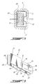
- Figure 1 of the appended drawings illustrates a device for connecting an electrical contact with a tab of a conductor, in particular but not exclusively a bus bar conductor.
- Device 1 comprises, in this preferred embodiment, a spring sleeve 2 and an electrically insulating tubular shroud 3.
- the spring sleeve 2 has the general configuration of a parallelepiped. More specifically, the spring sleeve 2 has a generally rectangular cross section, two opposite narrow walls 4 and 5, and two opposite wide walls 6 and 7. Wall 7 is formed with a central, axial slit 8 therein.
- Spring sleeve 2 is preferably made of a resilient conductive material such as spring metal. However, the use of other spring material to fabricate the sleeve 2 can also be contemplated.
- the slit 8 is delimited by two axially extending, parallel and mutually facing edge surfaces 9 and 10. From axial corner 11 to the edge surface 9, wide wall 7 slightly diverges inwardly, bends a first time inwardly at substantially right angle, and bends a second time at substantially right angle toward axial corner 12. From axial corner 12 to the edge surface 10, wide wall 7 slightly diverges inwardly, bends a first time inwardly at substantially right angle, and bends a second time at substantially right angle toward corner 11.
- this shape of the spring sleeve 2 produces a spring action allowing the spring sleeve 2 to apply a pressure on the tab and contact tails inserted therein.
- the above described shape of the wall 7 defines two axially coextending lips having respective inner faces 13 and 14 to apply this pressure on the tab and contact tails.
- the insulating shroud 3 is preferably made of electrically insulating material such as, for example, plastic material.
- the shroud 3 has a generally rectangular cross section and comprises, as illustrated in Figure 1, two opposite narrow walls 15 and 16 and two opposite wide walls 17 and 18.
- the internal dimensions of the shroud 3 are adapted to receive and fit the spring sleeve 2 in a first end section of the shroud 3 in an interface fit.
- Shroud 3 is therefore a captive, electrically insulating shroud which surrounds the spring sleeve 2 to prevent accidental electrocution. Since the insulating shroud 3 is longer than the spring sleeve 2, the spring sleeve 2 does not reside in the second remaining section of the shroud 3.
- the second section of the shroud 3 is formed with two symmetrical, axially extending slots such as 19 out-of-center in the two narrow walls 15 and 16, respectively.
- the device 1 can be used in relation to a generally flat bus bar conductor 20.
- the bus bar conductor 20 is formed with a tab 21. This tab 21 is inserted in the spring sleeve 2 through the second slotted section of the shroud 3. Upon insertion of tab 21 in spring sleeve 2, the flat bus bar conductor 20 is simultaneously introduced in the two slots such as 19 which form a seat for said bus bar conductor 20.
- the spring sleeve 2 forms a socket member which is smaller than tails 22 and 23 and tab 21.
- the resiliencey of sleeve 2 creates a semi permanent, high performance electrical contact at the interfaces between the contact tails 22 and 23 and the bus bar tab 21.
- the contact tails 22 and 23 may be equipped with one or more bosses (see axial bosses 24 in Figures 5 and 6) designed to concentrate the contact force on given regions of the interfaces between these contact tails 22 and 23 and the bus bar tab 21.
- both tails 22 and 23 and tab 21 extend into the opening 67 in PCB 46. Tails 22 and 23 extend entirely through opening 67 to the other side of PCB 46.
- spring sleeve 2 does not necessarily carry electric current.
- spring sleeve 2 can be an electrically conducting sleeve or an electrically insulating sleeve.
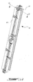
- Pass-thru bus bar contact 25 is made of a single piece of electrically conductive sheet metal cut and shaped as required.
- a similar "dual mass" contact is described in European Patent Application EP 0 951 102.
- Contact 25 further comprises a pair of generally flat and parallel contact members 26 and 27 defining mutually facing mating surfaces 28 and 29. As illustrated, the contact members 26 and 27 are generally parallel to the contact tails 22 and 23. Also, as illustrated in Figure 6, the spacing between the generally parallel contact members 26 and 27 is larger than the spacing between the parallel contact tails 22 and 23. However, it is within the scope of the present invention, as shown in Figure 15, to provide contact members 26 and 27 with a spacing between them which is larger than the spacing between the parallel contact tails 22 and 23.
- a transverse, curved bridge member 30 electrically and mechanically interconnects the contact members 26 and 27.
- Contact member 27 and contact tail 23 are interconnected through a pair of spaced apart and suitably curved bridge members 31 and 32.
- contact member 26 and contact tail 22 are interconnected through a pair of spaced apart and suitably curved bridge members of which only member 33 appears on Figure 6.
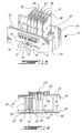
- the contact members 26 and 27 fit into a corresponding cavity 34 of an electrically insulating connector housing 35 made for example of injection-molded plastic material.
- the corresponding connector 36 is illustrated in Figures 7-11 of the appended drawings.
- the connector housing 35 comprises, as a non limitative example, a series of 6 laterally adjacent cavities 34.
- Each cavity 34 is designed to receive, from the rear of the connector housing, the contact 25 as indicated for example by the arrow 37 in Figure 8 to form an electrically conductive conductor-receiving receptacle.
- the rear face of the connector housing 35 is provided, around each opening 80 ( Figure 4) leading to a cavity 34 with beveled borders identified by the reference 81.
- each cavity 34 has a front peripheral inner border such as 38 to retain the contact members 26 and 27 in that cavity 34.
- connector 36 could comprise a pair of laterally adjacent, rectangular, and electrically conductive front receptacles 39 and 40.
- Figure 10 shows a cross sectional view of receptacle 39 taken along axis 10-10 of Figure 9.
- a pair of flat and opposite contact members such as 43 are mounted in a cavity 45 of the connector housing 35 to define the receptable 39.
- Each contact member 43 is provided with a set of 4 integral connection pins such as 44 extending rearwardly of the connector 36 for connection to through holes 70 in a printed circuit board (PCB) 46 (see Figures 4 and 13).
- Receptacle 40 is similar to receptacle 39.
- both contact members 43 and the corresponding cavity 45 are structured to fixedly mount the contact members 43 in the connector housing 35.
- Techniques for mounting the contact members 43 in the cavity 45 are believed to be otherwise well known to those of ordinary skill in the art, and accordingly will not be further described.
- the connector 36 could have a 4X8 matrix 41 of electrically conductive receptacle contacts such as 41 structured to receive electrically conductive pins (not shown) on the mating connector.
- Figure 11 shows a cross sectional view of a column of receptacle openings 42 taken along axis 11-11 of Figure 9.
- contact 41 has a mating section 47, for example a tubular spring contact member, disposed in a cavity 48 of the connector housing 35 to receive the mating pin contact.
- Each contact 41 also has an integral mounting section 49 extending rearwardly of the connector 36 for connection to a backplane PCB (Printed Circuit Board) 46 ( Figure 4).
- PCB Print Circuit Board
- each mating section 47 and the corresponding cavity 48 are structured to fixedly mount the contact in the cavity.
- Techniques for mounting each contact members 47 in the corresponding cavity 48 are believed to be otherwise well known to those of ordinary skill in the art, and accordingly will not be further described in the present specification.
- the connector 36 is secured to PCB 46 with hold-downs, each hold-down having barbed arms 50 extending rearwardly from the connector housing 35 for mechanically connecting the connector 36 to through holes 73 and 74 in the backplane PCB 46.
- a pair of slot openings such as 69 are provided on opposite sides of the connector housing 35 at the level of each cavity 34 and 45. These slot openings are provided for the purpose of ventilating the cavity and dissipating electrical contact heat.
- connector 36 is equipped with mixed PCB and pass-thru bus bar contacts.
- Electrical connector 36 can be a single- or multiblock (modular) separable connector equipped with mixed termination contacts; while some contacts attach to the backplane PCB through traditional means, e.g. solder, press-fit, etc., others pass through an opening cut in the backplane PCB to connect to a single or multiple bus bars running behind the PCB.
- Such a mix allows for a daughter board, equipped with the mating connector, to be fitted to the backplane PCB and send/receive power or signals to/from a common bus bar discretely situated behind the backplane PCB. This liberates space on the backplane PCB and allows for increased power distribution.
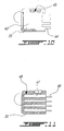
- Backplane bus bar system 51 can distribute power and signals to the components and/or daughter boards mounted on one or a series of backplane PCB's such as 52 and 53.
- the backplane bus bar system 51 may be insulated along the spine or wherever electrical signal contact is not required.
- the backplane bus bar system 51 may also be a laminated assembly to allow for a mix of signal frequencies, voltages, grounding, EMI (Electromagnetic Interference) shielding, etc.
- Backplane bus bar 51 comprises a pair of opposite elongated backplane PCB's 52 and 53.
- Backplane PCB 52 is mounted on a frame, preferably formed of a longitudinal metal plate 54 provided with symmetrical, opposite and longitudinal right angle flanges 55 and 56 to reinforce this metal plate.
- backplane PCB 53 is mounted on a frame, preferably formed of a longitudinal metal plate 57 provided with symmetrical, opposite and longitudinal right angle flanges 58 and 59 to reinforce this metal plate.
- transversal busbar conductor supports such as 58 mounted to the inner side of the metal plate 54 and such as 59 mounted on the inner side of the metal plate 57.
- Each support 58 and 59 is formed with a series of transversal grooves such as 60 to receive corresponding backplane bus bar conductors such as 61-66.
- a backplane busbar conductor is a generally flat bar of conductive metal with integral tabs such as 21 ( Figures 4 and 13). These tabs 21 make electrical connection with contacts 25 by, for example, solder connection (not shown), crimp connection (not shown), or the preferred method of the separable spring sleeve described above. As illustrated in Figure 13, opening such as 67 are cut in the backplane PCB's 52 and 53 and in the metal plate 54 and 57 to provide for access to these tabs 21.
- Conductor heat sinks such as 68 are finally provided to dissipate heat from at least some of the bus bar conductors 61-66.
- holes are provided in the backplane PCB's 52 and 53 at both ends of each opening 67.
- holes 70 will receive the pins 44 of receptacle 39
- holes 71 will receive the pins 44 of receptacle 40
- holes 72 will receive the pins 49 of the receptacles 42 of the matrix 41.
- the barbed arms 50 of the hold-down will hook in end holes 73 and 74 to mechanically connect and retain the connector 36 to the backplane PCB 52 or 53.
- the electrical connector 36 can be installed as follows:
- the pins 44 and 49 inserted in the holes 70-72 can be connected to the printed circuit of the PCB through soldering, press-fit, etc.
- the devices 1 and the pass-thru contacts 25 pass through the backplane PCB 46 and corresponding frame 54,57 without making electrical contact and preferably without physical contact.
- the spacing between the contact tails 22 and 23 is smaller than the spacing between the contact members 26 and 27.
- the spacing between the contact tails 22 and 23 is larger than the spacing between the contact members 26 and 27.
- bus bar conductors are discretely mounted beneath one or more backplane PCB's.
- Such a backplane bus bar arrangement and its location beneath the backplane PCB allow for increased power or signal distribution without sacrificing board space.
- bus bar conductors Although the preferred embodiments have been described with reference to bus bar conductors, it is within the scope of the present invention to use the device 1, contact 25 and connector 36 in relation to conductors other than bus bar conductors.
Landscapes
- Coupling Device And Connection With Printed Circuit (AREA)
- Details Of Connecting Devices For Male And Female Coupling (AREA)
- Multi-Conductor Connections (AREA)
Applications Claiming Priority (2)
| Application Number | Priority Date | Filing Date | Title |
|---|---|---|---|
| CA2351283 | 2001-06-22 | ||
| CA002351283A CA2351283A1 (en) | 2001-06-22 | 2001-06-22 | Connector assembly comprising a tab-receiving insulated spring sleeve and a dual contact pairs of spaced apart contact members and tails |
Publications (3)
| Publication Number | Publication Date |
|---|---|
| EP1294055A2 true EP1294055A2 (de) | 2003-03-19 |
| EP1294055A3 EP1294055A3 (de) | 2003-12-17 |
| EP1294055B1 EP1294055B1 (de) | 2006-03-15 |
Family
ID=4169338
Family Applications (1)
| Application Number | Title | Priority Date | Filing Date |
|---|---|---|---|
| EP02012381A Expired - Lifetime EP1294055B1 (de) | 2001-06-22 | 2002-06-06 | Steckverbinderanordnung mit einer Federbuchse und einem Doppelkontakt mit einem Paar von versetzten Kontaktelementen |
Country Status (8)
| Country | Link |
|---|---|
| US (1) | US6821164B2 (de) |
| EP (1) | EP1294055B1 (de) |
| JP (1) | JP2003036914A (de) |
| KR (1) | KR20030001271A (de) |
| AT (1) | ATE320667T1 (de) |
| CA (1) | CA2351283A1 (de) |
| DE (1) | DE60209833T8 (de) |
| TW (1) | TW555219U (de) |
Cited By (1)
| Publication number | Priority date | Publication date | Assignee | Title |
|---|---|---|---|---|
| CN104347971A (zh) * | 2013-08-08 | 2015-02-11 | 日本航空电子工业株式会社 | 连接器 |
Families Citing this family (8)
| Publication number | Priority date | Publication date | Assignee | Title |
|---|---|---|---|---|
| WO2008119393A1 (en) * | 2007-04-03 | 2008-10-09 | Telefonaktiebolaget Lm Ericsson (Publ) | Backplane to mate boards with different widths |
| US20110055247A1 (en) * | 2009-09-01 | 2011-03-03 | Blumberg Brad W | Provider-specific branding of generic mobile real estate search application |
| TWM534908U (zh) * | 2016-06-24 | 2017-01-01 | Bellwether Electronic Corp | 電源連接器及其電源端子 |
| US9716349B1 (en) * | 2016-08-15 | 2017-07-25 | Allsmartlite Technology Co., Ltd. | Electric connector |
| JP6720036B2 (ja) * | 2016-09-16 | 2020-07-08 | 日本航空電子工業株式会社 | コネクタ |
| FR3094578B1 (fr) | 2019-04-01 | 2021-12-10 | Aptiv Tech Ltd | Dispositif de connexion de puissance pour batterie électrique et ensemble de connexion comprenant ce dispositif. |
| TWI710167B (zh) * | 2019-11-04 | 2020-11-11 | 大陸商東莞訊滔電子有限公司 | 電連接器 |
| US12519261B2 (en) | 2021-07-06 | 2026-01-06 | Ennovi Industries, Inc. | Electrical coupler |
Family Cites Families (14)
| Publication number | Priority date | Publication date | Assignee | Title |
|---|---|---|---|---|
| US4755145A (en) * | 1982-11-12 | 1988-07-05 | Teradyne, Inc. | Electrically connecting circuit board system |
| US4472017A (en) * | 1983-04-01 | 1984-09-18 | Essex Group, Inc. | Tab receptacle terminal |
| US4954090A (en) * | 1988-05-31 | 1990-09-04 | Yazaki Corporation | Electric connection box |
| DE9106773U1 (de) * | 1991-06-03 | 1991-07-18 | Amp Inc., Harrisburg, Pa. | Elektrischer Steckkontakt |
| US5342226A (en) * | 1993-06-21 | 1994-08-30 | Electro-Wire Products, Inc. | Female blade terminal |
| AU667446B2 (en) * | 1993-09-16 | 1996-03-21 | Motorola, Inc. | Backplane with signal bus |
| US5486124A (en) * | 1994-08-04 | 1996-01-23 | Methode Electronics, Inc. | Rigid plastic hood for socket contacts |
| DE4446098C2 (de) * | 1994-12-22 | 1998-11-26 | Siemens Ag | Elektrischer Verbinder mit Abschirmung |
| US5639258A (en) * | 1995-05-15 | 1997-06-17 | Berg Technology, Inc. | Electrical connector including means for terminating wires |
| US5839906A (en) * | 1995-09-28 | 1998-11-24 | Emc Corporation | Data storage system |
| DE69718810T2 (de) * | 1996-10-29 | 2003-11-13 | The Whitaker Corp., Wilmington | Kontakt mit verriegelung zur kontakthalterung und dafür geeignetes gehaüse |
| DE19702233C2 (de) * | 1997-01-23 | 1999-09-30 | Phoenix Contact Gmbh & Co | Anschlußeinrichtung für ein elektrisches Gerät |
| CA2270564C (en) * | 1997-07-29 | 2006-03-14 | Hybricon Corporation | Connectors having improved crosstalk and signal transmission characteristics |
| US6319075B1 (en) * | 1998-04-17 | 2001-11-20 | Fci Americas Technology, Inc. | Power connector |
-
2001
- 2001-06-22 CA CA002351283A patent/CA2351283A1/en not_active Abandoned
-
2002
- 2002-05-31 TW TW091208047U patent/TW555219U/zh not_active IP Right Cessation
- 2002-06-06 DE DE60209833T patent/DE60209833T8/de not_active Expired - Fee Related
- 2002-06-06 EP EP02012381A patent/EP1294055B1/de not_active Expired - Lifetime
- 2002-06-06 AT AT02012381T patent/ATE320667T1/de not_active IP Right Cessation
- 2002-06-20 US US10/177,217 patent/US6821164B2/en not_active Expired - Fee Related
- 2002-06-21 JP JP2002181072A patent/JP2003036914A/ja active Pending
- 2002-06-21 KR KR1020020034742A patent/KR20030001271A/ko not_active Withdrawn
Cited By (1)
| Publication number | Priority date | Publication date | Assignee | Title |
|---|---|---|---|---|
| CN104347971A (zh) * | 2013-08-08 | 2015-02-11 | 日本航空电子工业株式会社 | 连接器 |
Also Published As
| Publication number | Publication date |
|---|---|
| DE60209833T2 (de) | 2006-12-14 |
| EP1294055B1 (de) | 2006-03-15 |
| DE60209833D1 (de) | 2006-05-11 |
| KR20030001271A (ko) | 2003-01-06 |
| US6821164B2 (en) | 2004-11-23 |
| CA2351283A1 (en) | 2002-12-22 |
| DE60209833T8 (de) | 2007-04-26 |
| EP1294055A3 (de) | 2003-12-17 |
| JP2003036914A (ja) | 2003-02-07 |
| ATE320667T1 (de) | 2006-04-15 |
| US20030082957A1 (en) | 2003-05-01 |
| TW555219U (en) | 2003-09-21 |
Similar Documents
| Publication | Publication Date | Title |
|---|---|---|
| CN113497397B (zh) | 一种连接器 | |
| US4867690A (en) | Electrical connector system | |
| EP0928049B1 (de) | Anreihverbinder für lokales Netzwerk | |
| EP1506597B1 (de) | Elektrischer stromverbinder | |
| US7824187B1 (en) | High density connector | |
| US5685739A (en) | Shielded electrical connector | |
| CN111883962B (zh) | 电连接器组件以及电连接器组合件 | |
| US5692928A (en) | Electrical connector having terminals with improved retention means | |
| US8328583B2 (en) | Power connector | |
| EP1964216B1 (de) | Verbinderfamilie für leiterplattenanbringungs- und kabelanwendungen | |
| US6994595B2 (en) | Finger proof, keyed power connector and methods thereof | |
| US8814605B2 (en) | Power connector | |
| US20250210893A1 (en) | Electric connector and assembly thereof with improved mounting features | |
| JP2869027B2 (ja) | 接続ピンのアラインメント装置及びこれと電気コネクタとの組み合わせ | |
| US5667411A (en) | Electrical connector having terminal alignment means | |
| US7413476B2 (en) | Electrical interconnection with mating terminals | |
| US6821164B2 (en) | Connector assembly comprising a tab-receiving insulated spring sleeve and a dual contact with pairs of spaced apart contact members and tails | |
| WO2021016454A1 (en) | Safe, robust, compact connector | |
| CN114336178A (zh) | 电连接器 | |
| CN205882239U (zh) | 插头连接器、插座连接器与连接器组件 | |
| CN215343053U (zh) | 端子和中央电器盒 | |
| US20260121363A1 (en) | Power connector with improved power terminals | |
| EP1020956A1 (de) | Oberflächenmontierbarer Steckverbinder mit einer verbesserten Anschlussklemmenanordnung | |
| CN115706371A (zh) | 直插式正交板对板连接器系统 | |
| JP3071686U (ja) | マルチリセプタクルの電気コネクタ |
Legal Events
| Date | Code | Title | Description |
|---|---|---|---|
| PUAI | Public reference made under article 153(3) epc to a published international application that has entered the european phase |
Free format text: ORIGINAL CODE: 0009012 |
|
| AK | Designated contracting states |
Kind code of ref document: A2 Designated state(s): AT BE CH CY DE DK ES FI FR GB GR IE IT LI LU MC NL PT SE TR Designated state(s): AT BE CH CY DE DK ES FI FR GB GR IE IT LI LU MC NL PT SE TR |
|
| AX | Request for extension of the european patent |
Extension state: AL LT LV MK RO SI |
|
| PUAL | Search report despatched |
Free format text: ORIGINAL CODE: 0009013 |
|
| AK | Designated contracting states |
Kind code of ref document: A3 Designated state(s): AT BE CH CY DE DK ES FI FR GB GR IE IT LI LU MC NL PT SE TR |
|
| AX | Request for extension of the european patent |
Extension state: AL LT LV MK RO SI |
|
| RIC1 | Information provided on ipc code assigned before grant |
Ipc: 7H 01R 31/06 B Ipc: 7H 01R 25/16 B Ipc: 7H 01R 13/18 B Ipc: 7H 01R 12/16 A |
|
| 17P | Request for examination filed |
Effective date: 20040608 |
|
| AKX | Designation fees paid |
Designated state(s): AT BE CH CY DE DK ES FI FR GB GR IE IT LI LU MC NL PT SE TR |
|
| 17Q | First examination report despatched |
Effective date: 20040812 |
|
| GRAP | Despatch of communication of intention to grant a patent |
Free format text: ORIGINAL CODE: EPIDOSNIGR1 |
|
| GRAS | Grant fee paid |
Free format text: ORIGINAL CODE: EPIDOSNIGR3 |
|
| GRAA | (expected) grant |
Free format text: ORIGINAL CODE: 0009210 |
|
| AK | Designated contracting states |
Kind code of ref document: B1 Designated state(s): AT BE CH CY DE DK ES FI FR GB GR IE IT LI LU MC NL PT SE TR |
|
| PG25 | Lapsed in a contracting state [announced via postgrant information from national office to epo] |
Ref country code: NL Free format text: LAPSE BECAUSE OF FAILURE TO SUBMIT A TRANSLATION OF THE DESCRIPTION OR TO PAY THE FEE WITHIN THE PRESCRIBED TIME-LIMIT Effective date: 20060315 Ref country code: LI Free format text: LAPSE BECAUSE OF FAILURE TO SUBMIT A TRANSLATION OF THE DESCRIPTION OR TO PAY THE FEE WITHIN THE PRESCRIBED TIME-LIMIT Effective date: 20060315 Ref country code: IT Free format text: LAPSE BECAUSE OF FAILURE TO SUBMIT A TRANSLATION OF THE DESCRIPTION OR TO PAY THE FEE WITHIN THE PRE;WARNING: LAPSES OF ITALIAN PATENTS WITH EFFECTIVE DATE BEFORE 2007 MAY HAVE OCCURRED AT ANY TIME BEFORE 2007. THE CORRECT EFFECTIVE DATE MAY BE DIFFERENT FROM THE ONE RECORDED.SCRIBED TIME-LIMIT Effective date: 20060315 Ref country code: FI Free format text: LAPSE BECAUSE OF FAILURE TO SUBMIT A TRANSLATION OF THE DESCRIPTION OR TO PAY THE FEE WITHIN THE PRESCRIBED TIME-LIMIT Effective date: 20060315 Ref country code: CH Free format text: LAPSE BECAUSE OF FAILURE TO SUBMIT A TRANSLATION OF THE DESCRIPTION OR TO PAY THE FEE WITHIN THE PRESCRIBED TIME-LIMIT Effective date: 20060315 Ref country code: AT Free format text: LAPSE BECAUSE OF FAILURE TO SUBMIT A TRANSLATION OF THE DESCRIPTION OR TO PAY THE FEE WITHIN THE PRESCRIBED TIME-LIMIT Effective date: 20060315 |
|
| REG | Reference to a national code |
Ref country code: GB Ref legal event code: FG4D Ref country code: CH Ref legal event code: EP |
|
| REG | Reference to a national code |
Ref country code: IE Ref legal event code: FG4D |
|
| RAP2 | Party data changed (patent owner data changed or rights of a patent transferred) |
Owner name: FCI EXPANSION 2 |
|
| REF | Corresponds to: |
Ref document number: 60209833 Country of ref document: DE Date of ref document: 20060511 Kind code of ref document: P |
|
| PG25 | Lapsed in a contracting state [announced via postgrant information from national office to epo] |
Ref country code: IE Free format text: LAPSE BECAUSE OF NON-PAYMENT OF DUE FEES Effective date: 20060606 |
|
| RAP2 | Party data changed (patent owner data changed or rights of a patent transferred) |
Owner name: IDEALEC |
|
| PG25 | Lapsed in a contracting state [announced via postgrant information from national office to epo] |
Ref country code: SE Free format text: LAPSE BECAUSE OF FAILURE TO SUBMIT A TRANSLATION OF THE DESCRIPTION OR TO PAY THE FEE WITHIN THE PRESCRIBED TIME-LIMIT Effective date: 20060615 Ref country code: DK Free format text: LAPSE BECAUSE OF FAILURE TO SUBMIT A TRANSLATION OF THE DESCRIPTION OR TO PAY THE FEE WITHIN THE PRESCRIBED TIME-LIMIT Effective date: 20060615 |
|
| PG25 | Lapsed in a contracting state [announced via postgrant information from national office to epo] |
Ref country code: ES Free format text: LAPSE BECAUSE OF FAILURE TO SUBMIT A TRANSLATION OF THE DESCRIPTION OR TO PAY THE FEE WITHIN THE PRESCRIBED TIME-LIMIT Effective date: 20060626 |
|
| PG25 | Lapsed in a contracting state [announced via postgrant information from national office to epo] |
Ref country code: MC Free format text: LAPSE BECAUSE OF NON-PAYMENT OF DUE FEES Effective date: 20060630 |
|
| NLT2 | Nl: modifications (of names), taken from the european patent patent bulletin |
Owner name: FCI EXPANSION 2 Effective date: 20060510 |
|
| NLT2 | Nl: modifications (of names), taken from the european patent patent bulletin |
Owner name: IDEALEC Effective date: 20060607 |
|
| PG25 | Lapsed in a contracting state [announced via postgrant information from national office to epo] |
Ref country code: PT Free format text: LAPSE BECAUSE OF FAILURE TO SUBMIT A TRANSLATION OF THE DESCRIPTION OR TO PAY THE FEE WITHIN THE PRESCRIBED TIME-LIMIT Effective date: 20060816 |
|
| NLV1 | Nl: lapsed or annulled due to failure to fulfill the requirements of art. 29p and 29m of the patents act | ||
| REG | Reference to a national code |
Ref country code: CH Ref legal event code: PL |
|
| ET | Fr: translation filed | ||
| PLBE | No opposition filed within time limit |
Free format text: ORIGINAL CODE: 0009261 |
|
| STAA | Information on the status of an ep patent application or granted ep patent |
Free format text: STATUS: NO OPPOSITION FILED WITHIN TIME LIMIT |
|
| 26N | No opposition filed |
Effective date: 20061218 |
|
| PGFP | Annual fee paid to national office [announced via postgrant information from national office to epo] |
Ref country code: DE Payment date: 20070612 Year of fee payment: 6 |
|
| PGFP | Annual fee paid to national office [announced via postgrant information from national office to epo] |
Ref country code: BE Payment date: 20070626 Year of fee payment: 6 |
|
| PGFP | Annual fee paid to national office [announced via postgrant information from national office to epo] |
Ref country code: GB Payment date: 20070619 Year of fee payment: 6 |
|
| BECA | Be: change of holder's address |
Owner name: *IDEALEC145/147 RUE YVES LE COZ, F-78000 VERSAILLE Effective date: 20060315 |
|
| BECN | Be: change of holder's name |
Owner name: *IDEALEC Effective date: 20060315 |
|
| PG25 | Lapsed in a contracting state [announced via postgrant information from national office to epo] |
Ref country code: GR Free format text: LAPSE BECAUSE OF FAILURE TO SUBMIT A TRANSLATION OF THE DESCRIPTION OR TO PAY THE FEE WITHIN THE PRESCRIBED TIME-LIMIT Effective date: 20060616 |
|
| PGFP | Annual fee paid to national office [announced via postgrant information from national office to epo] |
Ref country code: FR Payment date: 20070628 Year of fee payment: 6 |
|
| PG25 | Lapsed in a contracting state [announced via postgrant information from national office to epo] |
Ref country code: TR Free format text: LAPSE BECAUSE OF FAILURE TO SUBMIT A TRANSLATION OF THE DESCRIPTION OR TO PAY THE FEE WITHIN THE PRESCRIBED TIME-LIMIT Effective date: 20060315 Ref country code: LU Free format text: LAPSE BECAUSE OF NON-PAYMENT OF DUE FEES Effective date: 20060606 |
|
| PG25 | Lapsed in a contracting state [announced via postgrant information from national office to epo] |
Ref country code: CY Free format text: LAPSE BECAUSE OF FAILURE TO SUBMIT A TRANSLATION OF THE DESCRIPTION OR TO PAY THE FEE WITHIN THE PRESCRIBED TIME-LIMIT Effective date: 20060315 |
|
| BERE | Be: lapsed |
Owner name: *IDEALEC Effective date: 20080630 |
|
| GBPC | Gb: european patent ceased through non-payment of renewal fee |
Effective date: 20080606 |
|
| PG25 | Lapsed in a contracting state [announced via postgrant information from national office to epo] |
Ref country code: BE Free format text: LAPSE BECAUSE OF NON-PAYMENT OF DUE FEES Effective date: 20080630 |
|
| REG | Reference to a national code |
Ref country code: FR Ref legal event code: ST Effective date: 20090228 |
|
| PG25 | Lapsed in a contracting state [announced via postgrant information from national office to epo] |
Ref country code: DE Free format text: LAPSE BECAUSE OF NON-PAYMENT OF DUE FEES Effective date: 20090101 |
|
| PG25 | Lapsed in a contracting state [announced via postgrant information from national office to epo] |
Ref country code: GB Free format text: LAPSE BECAUSE OF NON-PAYMENT OF DUE FEES Effective date: 20080606 |
|
| PG25 | Lapsed in a contracting state [announced via postgrant information from national office to epo] |
Ref country code: FR Free format text: LAPSE BECAUSE OF NON-PAYMENT OF DUE FEES Effective date: 20080630 |