EP1293997B1 - Imidazolverbindungen und Elektrolytzusammensetzung für eine Farbstoffsolarzelle - Google Patents
Imidazolverbindungen und Elektrolytzusammensetzung für eine Farbstoffsolarzelle Download PDFInfo
- Publication number
- EP1293997B1 EP1293997B1 EP02019739A EP02019739A EP1293997B1 EP 1293997 B1 EP1293997 B1 EP 1293997B1 EP 02019739 A EP02019739 A EP 02019739A EP 02019739 A EP02019739 A EP 02019739A EP 1293997 B1 EP1293997 B1 EP 1293997B1
- Authority
- EP
- European Patent Office
- Prior art keywords
- dye
- layer
- photoelectric conversion
- semiconductor particles
- electrolytic composition
- Prior art date
- Legal status (The legal status is an assumption and is not a legal conclusion. Google has not performed a legal analysis and makes no representation as to the accuracy of the status listed.)
- Expired - Lifetime
Links
- 239000000203 mixture Substances 0.000 title claims abstract description 70
- 150000004693 imidazolium salts Chemical class 0.000 title description 3
- 238000006243 chemical reaction Methods 0.000 claims abstract description 71
- 150000003839 salts Chemical class 0.000 claims abstract description 53
- 239000003792 electrolyte Substances 0.000 claims abstract description 47
- XUIMIQQOPSSXEZ-UHFFFAOYSA-N Silicon Chemical group [Si] XUIMIQQOPSSXEZ-UHFFFAOYSA-N 0.000 claims abstract description 6
- 150000001450 anions Chemical class 0.000 claims abstract description 6
- 229910052710 silicon Inorganic materials 0.000 claims abstract description 6
- 239000004065 semiconductor Substances 0.000 claims description 85
- 239000002245 particle Substances 0.000 claims description 82
- GWEVSGVZZGPLCZ-UHFFFAOYSA-N Titan oxide Chemical compound O=[Ti]=O GWEVSGVZZGPLCZ-UHFFFAOYSA-N 0.000 claims description 51
- 238000012546 transfer Methods 0.000 claims description 36
- 239000011521 glass Substances 0.000 claims description 22
- 125000002496 methyl group Chemical group [H]C([H])([H])* 0.000 claims description 18
- 150000001875 compounds Chemical class 0.000 claims description 11
- RAXXELZNTBOGNW-UHFFFAOYSA-O Imidazolium Chemical class C1=C[NH+]=CN1 RAXXELZNTBOGNW-UHFFFAOYSA-O 0.000 claims description 7
- 125000004432 carbon atom Chemical group C* 0.000 claims description 6
- 125000005647 linker group Chemical group 0.000 claims description 6
- 125000001424 substituent group Chemical group 0.000 claims description 6
- 239000012327 Ruthenium complex Substances 0.000 claims description 5
- 125000000217 alkyl group Chemical group 0.000 claims description 5
- 239000013110 organic ligand Substances 0.000 claims description 2
- 150000001768 cations Chemical class 0.000 abstract description 3
- 239000010410 layer Substances 0.000 description 163
- 238000000034 method Methods 0.000 description 73
- 239000000975 dye Substances 0.000 description 54
- 239000000758 substrate Substances 0.000 description 41
- YMWUJEATGCHHMB-UHFFFAOYSA-N Dichloromethane Chemical compound ClCCl YMWUJEATGCHHMB-UHFFFAOYSA-N 0.000 description 30
- 229910052751 metal Inorganic materials 0.000 description 30
- 239000002184 metal Substances 0.000 description 30
- WEVYAHXRMPXWCK-UHFFFAOYSA-N Acetonitrile Chemical compound CC#N WEVYAHXRMPXWCK-UHFFFAOYSA-N 0.000 description 24
- OKKJLVBELUTLKV-UHFFFAOYSA-N Methanol Chemical compound OC OKKJLVBELUTLKV-UHFFFAOYSA-N 0.000 description 21
- 239000002904 solvent Substances 0.000 description 20
- XOLBLPGZBRYERU-UHFFFAOYSA-N tin dioxide Chemical compound O=[Sn]=O XOLBLPGZBRYERU-UHFFFAOYSA-N 0.000 description 18
- 239000000463 material Substances 0.000 description 17
- XLOMVQKBTHCTTD-UHFFFAOYSA-N Zinc monoxide Chemical compound [Zn]=O XLOMVQKBTHCTTD-UHFFFAOYSA-N 0.000 description 16
- 239000006185 dispersion Substances 0.000 description 16
- 238000000576 coating method Methods 0.000 description 15
- 238000010438 heat treatment Methods 0.000 description 15
- LFQSCWFLJHTTHZ-UHFFFAOYSA-N Ethanol Chemical compound CCO LFQSCWFLJHTTHZ-UHFFFAOYSA-N 0.000 description 13
- 239000000243 solution Substances 0.000 description 13
- ZKATWMILCYLAPD-UHFFFAOYSA-N niobium pentoxide Chemical compound O=[Nb](=O)O[Nb](=O)=O ZKATWMILCYLAPD-UHFFFAOYSA-N 0.000 description 12
- -1 ethylene glycol dialkylethers Chemical class 0.000 description 11
- 239000000178 monomer Substances 0.000 description 11
- BASFCYQUMIYNBI-UHFFFAOYSA-N platinum Chemical compound [Pt] BASFCYQUMIYNBI-UHFFFAOYSA-N 0.000 description 10
- XLYOFNOQVPJJNP-UHFFFAOYSA-N water Substances O XLYOFNOQVPJJNP-UHFFFAOYSA-N 0.000 description 10
- 239000011248 coating agent Substances 0.000 description 9
- ZCYVEMRRCGMTRW-UHFFFAOYSA-N 7553-56-2 Chemical compound [I] ZCYVEMRRCGMTRW-UHFFFAOYSA-N 0.000 description 8
- RTZKZFJDLAIYFH-UHFFFAOYSA-N Diethyl ether Chemical compound CCOCC RTZKZFJDLAIYFH-UHFFFAOYSA-N 0.000 description 8
- 239000011630 iodine Substances 0.000 description 8
- 229910052740 iodine Inorganic materials 0.000 description 8
- 229920000642 polymer Polymers 0.000 description 8
- 238000003980 solgel method Methods 0.000 description 8
- 239000000126 substance Substances 0.000 description 8
- 230000000052 comparative effect Effects 0.000 description 7
- LYCAIKOWRPUZTN-UHFFFAOYSA-N ethylene glycol Natural products OCCO LYCAIKOWRPUZTN-UHFFFAOYSA-N 0.000 description 7
- 150000002496 iodine Chemical class 0.000 description 7
- DNIAPMSPPWPWGF-UHFFFAOYSA-N monopropylene glycol Natural products CC(O)CO DNIAPMSPPWPWGF-UHFFFAOYSA-N 0.000 description 7
- 238000006116 polymerization reaction Methods 0.000 description 7
- ZNOKGRXACCSDPY-UHFFFAOYSA-N tungsten(VI) oxide Inorganic materials O=[W](=O)=O ZNOKGRXACCSDPY-UHFFFAOYSA-N 0.000 description 7
- CSCPPACGZOOCGX-UHFFFAOYSA-N Acetone Chemical compound CC(C)=O CSCPPACGZOOCGX-UHFFFAOYSA-N 0.000 description 6
- IAZDPXIOMUYVGZ-UHFFFAOYSA-N Dimethylsulphoxide Chemical compound CS(C)=O IAZDPXIOMUYVGZ-UHFFFAOYSA-N 0.000 description 6
- XEKOWRVHYACXOJ-UHFFFAOYSA-N Ethyl acetate Chemical compound CCOC(C)=O XEKOWRVHYACXOJ-UHFFFAOYSA-N 0.000 description 6
- 239000002202 Polyethylene glycol Substances 0.000 description 6
- BQCADISMDOOEFD-UHFFFAOYSA-N Silver Chemical compound [Ag] BQCADISMDOOEFD-UHFFFAOYSA-N 0.000 description 6
- 230000015572 biosynthetic process Effects 0.000 description 6
- 239000004020 conductor Substances 0.000 description 6
- 239000007788 liquid Substances 0.000 description 6
- 238000004519 manufacturing process Methods 0.000 description 6
- 229910044991 metal oxide Inorganic materials 0.000 description 6
- 150000004706 metal oxides Chemical class 0.000 description 6
- 229920001223 polyethylene glycol Polymers 0.000 description 6
- 238000007639 printing Methods 0.000 description 6
- 229910052709 silver Inorganic materials 0.000 description 6
- 239000004332 silver Substances 0.000 description 6
- 238000002791 soaking Methods 0.000 description 6
- 239000007787 solid Substances 0.000 description 6
- 238000003786 synthesis reaction Methods 0.000 description 6
- 239000004408 titanium dioxide Substances 0.000 description 6
- 238000007740 vapor deposition Methods 0.000 description 6
- RYGMFSIKBFXOCR-UHFFFAOYSA-N Copper Chemical compound [Cu] RYGMFSIKBFXOCR-UHFFFAOYSA-N 0.000 description 5
- HCHKCACWOHOZIP-UHFFFAOYSA-N Zinc Chemical compound [Zn] HCHKCACWOHOZIP-UHFFFAOYSA-N 0.000 description 5
- 229910052782 aluminium Inorganic materials 0.000 description 5
- XAGFODPZIPBFFR-UHFFFAOYSA-N aluminium Chemical compound [Al] XAGFODPZIPBFFR-UHFFFAOYSA-N 0.000 description 5
- 229910052802 copper Inorganic materials 0.000 description 5
- 239000010949 copper Substances 0.000 description 5
- PCHJSUWPFVWCPO-UHFFFAOYSA-N gold Chemical compound [Au] PCHJSUWPFVWCPO-UHFFFAOYSA-N 0.000 description 5
- 229910052737 gold Inorganic materials 0.000 description 5
- 239000010931 gold Substances 0.000 description 5
- JEIPFZHSYJVQDO-UHFFFAOYSA-N iron(III) oxide Inorganic materials O=[Fe]O[Fe]=O JEIPFZHSYJVQDO-UHFFFAOYSA-N 0.000 description 5
- 229910052697 platinum Inorganic materials 0.000 description 5
- 238000001179 sorption measurement Methods 0.000 description 5
- 229910052725 zinc Inorganic materials 0.000 description 5
- 239000011701 zinc Substances 0.000 description 5
- OKTJSMMVPCPJKN-UHFFFAOYSA-N Carbon Chemical compound [C] OKTJSMMVPCPJKN-UHFFFAOYSA-N 0.000 description 4
- JUJWROOIHBZHMG-UHFFFAOYSA-N Pyridine Chemical class C1=CC=NC=C1 JUJWROOIHBZHMG-UHFFFAOYSA-N 0.000 description 4
- VYPSYNLAJGMNEJ-UHFFFAOYSA-N Silicium dioxide Chemical compound O=[Si]=O VYPSYNLAJGMNEJ-UHFFFAOYSA-N 0.000 description 4
- 229910002370 SrTiO3 Inorganic materials 0.000 description 4
- RTAQQCXQSZGOHL-UHFFFAOYSA-N Titanium Chemical compound [Ti] RTAQQCXQSZGOHL-UHFFFAOYSA-N 0.000 description 4
- MCMNRKCIXSYSNV-UHFFFAOYSA-N Zirconium dioxide Chemical compound O=[Zr]=O MCMNRKCIXSYSNV-UHFFFAOYSA-N 0.000 description 4
- 239000002131 composite material Substances 0.000 description 4
- 238000004132 cross linking Methods 0.000 description 4
- 239000008151 electrolyte solution Substances 0.000 description 4
- 229940021013 electrolyte solution Drugs 0.000 description 4
- 229910052738 indium Inorganic materials 0.000 description 4
- APFVFJFRJDLVQX-UHFFFAOYSA-N indium atom Chemical compound [In] APFVFJFRJDLVQX-UHFFFAOYSA-N 0.000 description 4
- 239000011244 liquid electrolyte Substances 0.000 description 4
- 238000001819 mass spectrum Methods 0.000 description 4
- 238000002844 melting Methods 0.000 description 4
- 239000000434 metal complex dye Substances 0.000 description 4
- 239000003960 organic solvent Substances 0.000 description 4
- 229920003023 plastic Polymers 0.000 description 4
- 239000004033 plastic Substances 0.000 description 4
- 238000007747 plating Methods 0.000 description 4
- 238000010526 radical polymerization reaction Methods 0.000 description 4
- 229910001887 tin oxide Inorganic materials 0.000 description 4
- 229910052719 titanium Inorganic materials 0.000 description 4
- 239000010936 titanium Substances 0.000 description 4
- 238000005406 washing Methods 0.000 description 4
- OISVCGZHLKNMSJ-UHFFFAOYSA-N 2,6-dimethylpyridine Chemical compound CC1=CC=CC(C)=N1 OISVCGZHLKNMSJ-UHFFFAOYSA-N 0.000 description 3
- JBRZTFJDHDCESZ-UHFFFAOYSA-N AsGa Chemical compound [As]#[Ga] JBRZTFJDHDCESZ-UHFFFAOYSA-N 0.000 description 3
- UHOVQNZJYSORNB-UHFFFAOYSA-N Benzene Chemical compound C1=CC=CC=C1 UHOVQNZJYSORNB-UHFFFAOYSA-N 0.000 description 3
- WVDDGKGOMKODPV-UHFFFAOYSA-N Benzyl alcohol Chemical compound OCC1=CC=CC=C1 WVDDGKGOMKODPV-UHFFFAOYSA-N 0.000 description 3
- KFZMGEQAYNKOFK-UHFFFAOYSA-N Isopropanol Chemical compound CC(C)O KFZMGEQAYNKOFK-UHFFFAOYSA-N 0.000 description 3
- WMFOQBRAJBCJND-UHFFFAOYSA-M Lithium hydroxide Chemical compound [Li+].[OH-] WMFOQBRAJBCJND-UHFFFAOYSA-M 0.000 description 3
- ZMXDDKWLCZADIW-UHFFFAOYSA-N N,N-Dimethylformamide Chemical compound CN(C)C=O ZMXDDKWLCZADIW-UHFFFAOYSA-N 0.000 description 3
- YXFVVABEGXRONW-UHFFFAOYSA-N Toluene Chemical compound CC1=CC=CC=C1 YXFVVABEGXRONW-UHFFFAOYSA-N 0.000 description 3
- ZMANZCXQSJIPKH-UHFFFAOYSA-N Triethylamine Chemical compound CCN(CC)CC ZMANZCXQSJIPKH-UHFFFAOYSA-N 0.000 description 3
- 239000000654 additive Substances 0.000 description 3
- 239000002390 adhesive tape Substances 0.000 description 3
- 229910052787 antimony Inorganic materials 0.000 description 3
- WATWJIUSRGPENY-UHFFFAOYSA-N antimony atom Chemical compound [Sb] WATWJIUSRGPENY-UHFFFAOYSA-N 0.000 description 3
- JFDZBHWFFUWGJE-UHFFFAOYSA-N benzonitrile Chemical compound N#CC1=CC=CC=C1 JFDZBHWFFUWGJE-UHFFFAOYSA-N 0.000 description 3
- 229910052793 cadmium Inorganic materials 0.000 description 3
- BDOSMKKIYDKNTQ-UHFFFAOYSA-N cadmium atom Chemical compound [Cd] BDOSMKKIYDKNTQ-UHFFFAOYSA-N 0.000 description 3
- 229910052799 carbon Inorganic materials 0.000 description 3
- 125000003178 carboxy group Chemical group [H]OC(*)=O 0.000 description 3
- 238000005266 casting Methods 0.000 description 3
- 238000000151 deposition Methods 0.000 description 3
- 239000003480 eluent Substances 0.000 description 3
- 150000002170 ethers Chemical class 0.000 description 3
- 229940052303 ethers for general anesthesia Drugs 0.000 description 3
- 229940093476 ethylene glycol Drugs 0.000 description 3
- 239000000499 gel Substances 0.000 description 3
- 239000003349 gelling agent Substances 0.000 description 3
- 150000002500 ions Chemical class 0.000 description 3
- 230000008018 melting Effects 0.000 description 3
- VLKZOEOYAKHREP-UHFFFAOYSA-N n-Hexane Chemical compound CCCCCC VLKZOEOYAKHREP-UHFFFAOYSA-N 0.000 description 3
- 229910052757 nitrogen Inorganic materials 0.000 description 3
- 125000004433 nitrogen atom Chemical group N* 0.000 description 3
- 150000002892 organic cations Chemical class 0.000 description 3
- 150000002894 organic compounds Chemical class 0.000 description 3
- 239000012074 organic phase Substances 0.000 description 3
- 229920006254 polymer film Polymers 0.000 description 3
- 229920001451 polypropylene glycol Polymers 0.000 description 3
- 150000003346 selenoethers Chemical class 0.000 description 3
- 239000000741 silica gel Substances 0.000 description 3
- 229910002027 silica gel Inorganic materials 0.000 description 3
- 239000007784 solid electrolyte Substances 0.000 description 3
- 238000004528 spin coating Methods 0.000 description 3
- 238000004544 sputter deposition Methods 0.000 description 3
- 238000002834 transmittance Methods 0.000 description 3
- 125000001425 triazolyl group Chemical group 0.000 description 3
- MYRTYDVEIRVNKP-UHFFFAOYSA-N 1,2-Divinylbenzene Chemical compound C=CC1=CC=CC=C1C=C MYRTYDVEIRVNKP-UHFFFAOYSA-N 0.000 description 2
- WPWHSFAFEBZWBB-UHFFFAOYSA-N 1-butyl radical Chemical compound [CH2]CCC WPWHSFAFEBZWBB-UHFFFAOYSA-N 0.000 description 2
- LEJBBGNFPAFPKQ-UHFFFAOYSA-N 2-(2-prop-2-enoyloxyethoxy)ethyl prop-2-enoate Chemical compound C=CC(=O)OCCOCCOC(=O)C=C LEJBBGNFPAFPKQ-UHFFFAOYSA-N 0.000 description 2
- XFCMNSHQOZQILR-UHFFFAOYSA-N 2-[2-(2-methylprop-2-enoyloxy)ethoxy]ethyl 2-methylprop-2-enoate Chemical compound CC(=C)C(=O)OCCOCCOC(=O)C(C)=C XFCMNSHQOZQILR-UHFFFAOYSA-N 0.000 description 2
- BSKHPKMHTQYZBB-UHFFFAOYSA-N 2-methylpyridine Chemical compound CC1=CC=CC=N1 BSKHPKMHTQYZBB-UHFFFAOYSA-N 0.000 description 2
- KUDUQBURMYMBIJ-UHFFFAOYSA-N 2-prop-2-enoyloxyethyl prop-2-enoate Chemical compound C=CC(=O)OCCOC(=O)C=C KUDUQBURMYMBIJ-UHFFFAOYSA-N 0.000 description 2
- VWIIJDNADIEEDB-UHFFFAOYSA-N 3-methyl-1,3-oxazolidin-2-one Chemical compound CN1CCOC1=O VWIIJDNADIEEDB-UHFFFAOYSA-N 0.000 description 2
- YSHMQTRICHYLGF-UHFFFAOYSA-N 4-tert-butylpyridine Chemical compound CC(C)(C)C1=CC=NC=C1 YSHMQTRICHYLGF-UHFFFAOYSA-N 0.000 description 2
- 229920002284 Cellulose triacetate Polymers 0.000 description 2
- HEDRZPFGACZZDS-UHFFFAOYSA-N Chloroform Chemical compound ClC(Cl)Cl HEDRZPFGACZZDS-UHFFFAOYSA-N 0.000 description 2
- KMTRUDSVKNLOMY-UHFFFAOYSA-N Ethylene carbonate Chemical compound O=C1OCCO1 KMTRUDSVKNLOMY-UHFFFAOYSA-N 0.000 description 2
- PXGOKWXKJXAPGV-UHFFFAOYSA-N Fluorine Chemical compound FF PXGOKWXKJXAPGV-UHFFFAOYSA-N 0.000 description 2
- 229910001218 Gallium arsenide Inorganic materials 0.000 description 2
- PEDCQBHIVMGVHV-UHFFFAOYSA-N Glycerine Chemical compound OCC(O)CO PEDCQBHIVMGVHV-UHFFFAOYSA-N 0.000 description 2
- XEEYBQQBJWHFJM-UHFFFAOYSA-N Iron Chemical compound [Fe] XEEYBQQBJWHFJM-UHFFFAOYSA-N 0.000 description 2
- FYYHWMGAXLPEAU-UHFFFAOYSA-N Magnesium Chemical compound [Mg] FYYHWMGAXLPEAU-UHFFFAOYSA-N 0.000 description 2
- PXHVJJICTQNCMI-UHFFFAOYSA-N Nickel Chemical compound [Ni] PXHVJJICTQNCMI-UHFFFAOYSA-N 0.000 description 2
- 239000004697 Polyetherimide Substances 0.000 description 2
- 239000004642 Polyimide Substances 0.000 description 2
- 239000004734 Polyphenylene sulfide Substances 0.000 description 2
- 206010070834 Sensitisation Diseases 0.000 description 2
- QAOWNCQODCNURD-UHFFFAOYSA-N Sulfuric acid Chemical compound OS(O)(=O)=O QAOWNCQODCNURD-UHFFFAOYSA-N 0.000 description 2
- 229920010524 Syndiotactic polystyrene Polymers 0.000 description 2
- DKGAVHZHDRPRBM-UHFFFAOYSA-N Tert-Butanol Chemical compound CC(C)(C)O DKGAVHZHDRPRBM-UHFFFAOYSA-N 0.000 description 2
- WYURNTSHIVDZCO-UHFFFAOYSA-N Tetrahydrofuran Chemical compound C1CCOC1 WYURNTSHIVDZCO-UHFFFAOYSA-N 0.000 description 2
- NNLVGZFZQQXQNW-ADJNRHBOSA-N [(2r,3r,4s,5r,6s)-4,5-diacetyloxy-3-[(2s,3r,4s,5r,6r)-3,4,5-triacetyloxy-6-(acetyloxymethyl)oxan-2-yl]oxy-6-[(2r,3r,4s,5r,6s)-4,5,6-triacetyloxy-2-(acetyloxymethyl)oxan-3-yl]oxyoxan-2-yl]methyl acetate Chemical compound O([C@@H]1O[C@@H]([C@H]([C@H](OC(C)=O)[C@H]1OC(C)=O)O[C@H]1[C@@H]([C@@H](OC(C)=O)[C@H](OC(C)=O)[C@@H](COC(C)=O)O1)OC(C)=O)COC(=O)C)[C@@H]1[C@@H](COC(C)=O)O[C@@H](OC(C)=O)[C@H](OC(C)=O)[C@H]1OC(C)=O NNLVGZFZQQXQNW-ADJNRHBOSA-N 0.000 description 2
- 239000002253 acid Substances 0.000 description 2
- 150000001298 alcohols Chemical class 0.000 description 2
- 150000001346 alkyl aryl ethers Chemical class 0.000 description 2
- 229910045601 alloy Inorganic materials 0.000 description 2
- 239000000956 alloy Substances 0.000 description 2
- 150000001408 amides Chemical group 0.000 description 2
- 125000004429 atom Chemical group 0.000 description 2
- QVGXLLKOCUKJST-UHFFFAOYSA-N atomic oxygen Chemical compound [O] QVGXLLKOCUKJST-UHFFFAOYSA-N 0.000 description 2
- 150000007514 bases Chemical class 0.000 description 2
- 239000011324 bead Substances 0.000 description 2
- 229910052980 cadmium sulfide Inorganic materials 0.000 description 2
- UHYPYGJEEGLRJD-UHFFFAOYSA-N cadmium(2+);selenium(2-) Chemical compound [Se-2].[Cd+2] UHYPYGJEEGLRJD-UHFFFAOYSA-N 0.000 description 2
- LYQFWZFBNBDLEO-UHFFFAOYSA-M caesium bromide Chemical compound [Br-].[Cs+] LYQFWZFBNBDLEO-UHFFFAOYSA-M 0.000 description 2
- 150000004649 carbonic acid derivatives Chemical class 0.000 description 2
- 239000000919 ceramic Substances 0.000 description 2
- 150000004770 chalcogenides Chemical class 0.000 description 2
- 239000007810 chemical reaction solvent Substances 0.000 description 2
- 238000005229 chemical vapour deposition Methods 0.000 description 2
- 150000001805 chlorine compounds Chemical class 0.000 description 2
- MVPPADPHJFYWMZ-UHFFFAOYSA-N chlorobenzene Chemical compound ClC1=CC=CC=C1 MVPPADPHJFYWMZ-UHFFFAOYSA-N 0.000 description 2
- QMVPMAAFGQKVCJ-UHFFFAOYSA-N citronellol Chemical compound OCCC(C)CCC=C(C)C QMVPMAAFGQKVCJ-UHFFFAOYSA-N 0.000 description 2
- 239000003431 cross linking reagent Substances 0.000 description 2
- JHIVVAPYMSGYDF-UHFFFAOYSA-N cyclohexanone Chemical compound O=C1CCCCC1 JHIVVAPYMSGYDF-UHFFFAOYSA-N 0.000 description 2
- 150000001983 dialkylethers Chemical class 0.000 description 2
- 229960004132 diethyl ether Drugs 0.000 description 2
- 238000007598 dipping method Methods 0.000 description 2
- 239000002270 dispersing agent Substances 0.000 description 2
- 238000009826 distribution Methods 0.000 description 2
- 230000005518 electrochemistry Effects 0.000 description 2
- 238000005516 engineering process Methods 0.000 description 2
- 150000002148 esters Chemical class 0.000 description 2
- 230000001747 exhibiting effect Effects 0.000 description 2
- 238000001125 extrusion Methods 0.000 description 2
- 239000011737 fluorine Substances 0.000 description 2
- 229910052731 fluorine Inorganic materials 0.000 description 2
- 229910052949 galena Inorganic materials 0.000 description 2
- 239000007789 gas Substances 0.000 description 2
- 239000011245 gel electrolyte Substances 0.000 description 2
- 230000007062 hydrolysis Effects 0.000 description 2
- 238000006460 hydrolysis reaction Methods 0.000 description 2
- RHZWSUVWRRXEJF-UHFFFAOYSA-N indium tin Chemical compound [In].[Sn] RHZWSUVWRRXEJF-UHFFFAOYSA-N 0.000 description 2
- 239000002346 layers by function Substances 0.000 description 2
- AMXOYNBUYSYVKV-UHFFFAOYSA-M lithium bromide Chemical compound [Li+].[Br-] AMXOYNBUYSYVKV-UHFFFAOYSA-M 0.000 description 2
- 229910001416 lithium ion Inorganic materials 0.000 description 2
- 230000007774 longterm Effects 0.000 description 2
- 239000011777 magnesium Substances 0.000 description 2
- 229910052749 magnesium Inorganic materials 0.000 description 2
- 239000012702 metal oxide precursor Substances 0.000 description 2
- 150000002739 metals Chemical class 0.000 description 2
- 150000002825 nitriles Chemical class 0.000 description 2
- 239000001301 oxygen Substances 0.000 description 2
- 229910052760 oxygen Inorganic materials 0.000 description 2
- 239000002798 polar solvent Substances 0.000 description 2
- 229920002492 poly(sulfone) Polymers 0.000 description 2
- 229920001230 polyarylate Polymers 0.000 description 2
- 229920001601 polyetherimide Polymers 0.000 description 2
- 229920000139 polyethylene terephthalate Polymers 0.000 description 2
- 239000005020 polyethylene terephthalate Substances 0.000 description 2
- 229920001721 polyimide Polymers 0.000 description 2
- 239000003505 polymerization initiator Substances 0.000 description 2
- 229920000069 polyphenylene sulfide Polymers 0.000 description 2
- IOLCXVTUBQKXJR-UHFFFAOYSA-M potassium bromide Chemical compound [K+].[Br-] IOLCXVTUBQKXJR-UHFFFAOYSA-M 0.000 description 2
- 230000001376 precipitating effect Effects 0.000 description 2
- 238000002360 preparation method Methods 0.000 description 2
- FVSKHRXBFJPNKK-UHFFFAOYSA-N propionitrile Chemical compound CCC#N FVSKHRXBFJPNKK-UHFFFAOYSA-N 0.000 description 2
- RUOJZAUFBMNUDX-UHFFFAOYSA-N propylene carbonate Chemical compound CC1COC(=O)O1 RUOJZAUFBMNUDX-UHFFFAOYSA-N 0.000 description 2
- 230000009257 reactivity Effects 0.000 description 2
- 230000002441 reversible effect Effects 0.000 description 2
- 230000008313 sensitization Effects 0.000 description 2
- 239000002356 single layer Substances 0.000 description 2
- JHJLBTNAGRQEKS-UHFFFAOYSA-M sodium bromide Chemical compound [Na+].[Br-] JHJLBTNAGRQEKS-UHFFFAOYSA-M 0.000 description 2
- 238000003860 storage Methods 0.000 description 2
- 150000003871 sulfonates Chemical class 0.000 description 2
- QHGNHLZPVBIIPX-UHFFFAOYSA-N tin(ii) oxide Chemical class [Sn]=O QHGNHLZPVBIIPX-UHFFFAOYSA-N 0.000 description 2
- 238000001771 vacuum deposition Methods 0.000 description 2
- RUDATBOHQWOJDD-UHFFFAOYSA-N (3beta,5beta,7alpha)-3,7-Dihydroxycholan-24-oic acid Natural products OC1CC2CC(O)CCC2(C)C2C1C1CCC(C(CCC(O)=O)C)C1(C)CC2 RUDATBOHQWOJDD-UHFFFAOYSA-N 0.000 description 1
- QMVPMAAFGQKVCJ-SNVBAGLBSA-N (R)-(+)-citronellol Natural products OCC[C@H](C)CCC=C(C)C QMVPMAAFGQKVCJ-SNVBAGLBSA-N 0.000 description 1
- SCYULBFZEHDVBN-UHFFFAOYSA-N 1,1-Dichloroethane Chemical compound CC(Cl)Cl SCYULBFZEHDVBN-UHFFFAOYSA-N 0.000 description 1
- CYSGHNMQYZDMIA-UHFFFAOYSA-N 1,3-Dimethyl-2-imidazolidinon Chemical compound CN1CCN(C)C1=O CYSGHNMQYZDMIA-UHFFFAOYSA-N 0.000 description 1
- RYHBNJHYFVUHQT-UHFFFAOYSA-N 1,4-Dioxane Chemical compound C1COCCO1 RYHBNJHYFVUHQT-UHFFFAOYSA-N 0.000 description 1
- GWQYPLXGJIXMMV-UHFFFAOYSA-M 1-ethyl-3-methylimidazol-3-ium;bromide Chemical compound [Br-].CCN1C=C[N+](C)=C1 GWQYPLXGJIXMMV-UHFFFAOYSA-M 0.000 description 1
- ABFDKXBSQCTIKH-UHFFFAOYSA-M 1-ethylpyridin-1-ium;bromide Chemical compound [Br-].CC[N+]1=CC=CC=C1 ABFDKXBSQCTIKH-UHFFFAOYSA-M 0.000 description 1
- HQJLEFDAYKUXSA-UHFFFAOYSA-N 2,3-dihydroxycyclohexa-2,5-diene-1,4-dione Chemical compound OC1=C(O)C(=O)C=CC1=O HQJLEFDAYKUXSA-UHFFFAOYSA-N 0.000 description 1
- NTFJXDRAVMOYBG-UHFFFAOYSA-N 2-(2,2-dicyanoethoxymethyl)propanedinitrile Chemical compound N#CC(C#N)COCC(C#N)C#N NTFJXDRAVMOYBG-UHFFFAOYSA-N 0.000 description 1
- ZWEHNKRNPOVVGH-UHFFFAOYSA-N 2-Butanone Chemical compound CCC(C)=O ZWEHNKRNPOVVGH-UHFFFAOYSA-N 0.000 description 1
- QKPVEISEHYYHRH-UHFFFAOYSA-N 2-methoxyacetonitrile Chemical compound COCC#N QKPVEISEHYYHRH-UHFFFAOYSA-N 0.000 description 1
- XWKFPIODWVPXLX-UHFFFAOYSA-N 2-methyl-5-methylpyridine Natural products CC1=CC=C(C)N=C1 XWKFPIODWVPXLX-UHFFFAOYSA-N 0.000 description 1
- UUIMDJFBHNDZOW-UHFFFAOYSA-N 2-tert-butylpyridine Chemical compound CC(C)(C)C1=CC=CC=N1 UUIMDJFBHNDZOW-UHFFFAOYSA-N 0.000 description 1
- HTWRFCRQSLVESJ-UHFFFAOYSA-N 3-(2-methylprop-2-enoyloxy)propyl 2-methylprop-2-enoate Chemical compound CC(=C)C(=O)OCCCOC(=O)C(C)=C HTWRFCRQSLVESJ-UHFFFAOYSA-N 0.000 description 1
- OOWFYDWAMOKVSF-UHFFFAOYSA-N 3-methoxypropanenitrile Chemical compound COCCC#N OOWFYDWAMOKVSF-UHFFFAOYSA-N 0.000 description 1
- GFLJTEHFZZNCTR-UHFFFAOYSA-N 3-prop-2-enoyloxypropyl prop-2-enoate Chemical compound C=CC(=O)OCCCOC(=O)C=C GFLJTEHFZZNCTR-UHFFFAOYSA-N 0.000 description 1
- ULAQNFFHUVUDJG-UHFFFAOYSA-N 3-trimethylsilylpropane-1-sulfonic acid hydrochloride Chemical compound Cl.C[Si](C)(C)CCCS(O)(=O)=O ULAQNFFHUVUDJG-UHFFFAOYSA-N 0.000 description 1
- DBCAQXHNJOFNGC-UHFFFAOYSA-N 4-bromo-1,1,1-trifluorobutane Chemical compound FC(F)(F)CCCBr DBCAQXHNJOFNGC-UHFFFAOYSA-N 0.000 description 1
- MARUHZGHZWCEQU-UHFFFAOYSA-N 5-phenyl-2h-tetrazole Chemical compound C1=CC=CC=C1C1=NNN=N1 MARUHZGHZWCEQU-UHFFFAOYSA-N 0.000 description 1
- GMVPRGQOIOIIMI-DODZYUBVSA-N 7-[(1R,2R,3R)-3-hydroxy-2-[(3S)-3-hydroxyoct-1-enyl]-5-oxocyclopentyl]heptanoic acid Chemical compound CCCCC[C@H](O)C=C[C@H]1[C@H](O)CC(=O)[C@@H]1CCCCCCC(O)=O GMVPRGQOIOIIMI-DODZYUBVSA-N 0.000 description 1
- 229910002012 Aerosil® Inorganic materials 0.000 description 1
- 238000012935 Averaging Methods 0.000 description 1
- CPELXLSAUQHCOX-UHFFFAOYSA-M Bromide Chemical compound [Br-] CPELXLSAUQHCOX-UHFFFAOYSA-M 0.000 description 1
- DKPFZGUDAPQIHT-UHFFFAOYSA-N Butyl acetate Natural products CCCCOC(C)=O DKPFZGUDAPQIHT-UHFFFAOYSA-N 0.000 description 1
- 0 CCC(CC(*)[N+](*)*)N=O Chemical compound CCC(CC(*)[N+](*)*)N=O 0.000 description 1
- UNMYWSMUMWPJLR-UHFFFAOYSA-L Calcium iodide Chemical compound [Ca+2].[I-].[I-] UNMYWSMUMWPJLR-UHFFFAOYSA-L 0.000 description 1
- 229920002134 Carboxymethyl cellulose Polymers 0.000 description 1
- 229910004613 CdTe Inorganic materials 0.000 description 1
- 229910052684 Cerium Inorganic materials 0.000 description 1
- ZAMOUSCENKQFHK-UHFFFAOYSA-N Chlorine atom Chemical compound [Cl] ZAMOUSCENKQFHK-UHFFFAOYSA-N 0.000 description 1
- OIFBSDVPJOWBCH-UHFFFAOYSA-N Diethyl carbonate Chemical compound CCOC(=O)OCC OIFBSDVPJOWBCH-UHFFFAOYSA-N 0.000 description 1
- 239000004593 Epoxy Substances 0.000 description 1
- 229910005540 GaP Inorganic materials 0.000 description 1
- GYHNNYVSQQEPJS-UHFFFAOYSA-N Gallium Chemical compound [Ga] GYHNNYVSQQEPJS-UHFFFAOYSA-N 0.000 description 1
- 239000004354 Hydroxyethyl cellulose Substances 0.000 description 1
- 229920000663 Hydroxyethyl cellulose Polymers 0.000 description 1
- HBBGRARXTFLTSG-UHFFFAOYSA-N Lithium ion Chemical compound [Li+] HBBGRARXTFLTSG-UHFFFAOYSA-N 0.000 description 1
- 229910016287 MxOy Inorganic materials 0.000 description 1
- FXHOOIRPVKKKFG-UHFFFAOYSA-N N,N-Dimethylacetamide Chemical compound CN(C)C(C)=O FXHOOIRPVKKKFG-UHFFFAOYSA-N 0.000 description 1
- SECXISVLQFMRJM-UHFFFAOYSA-N N-Methylpyrrolidone Chemical compound CN1CCCC1=O SECXISVLQFMRJM-UHFFFAOYSA-N 0.000 description 1
- VCUFZILGIRCDQQ-KRWDZBQOSA-N N-[[(5S)-2-oxo-3-(2-oxo-3H-1,3-benzoxazol-6-yl)-1,3-oxazolidin-5-yl]methyl]-2-[[3-(trifluoromethoxy)phenyl]methylamino]pyrimidine-5-carboxamide Chemical compound O=C1O[C@H](CN1C1=CC2=C(NC(O2)=O)C=C1)CNC(=O)C=1C=NC(=NC=1)NCC1=CC(=CC=C1)OC(F)(F)F VCUFZILGIRCDQQ-KRWDZBQOSA-N 0.000 description 1
- FXPLCAKVOYHAJA-UHFFFAOYSA-N OC(c1ccnc(-c2cc(C(O)=O)ccn2)c1)=O Chemical compound OC(c1ccnc(-c2cc(C(O)=O)ccn2)c1)=O FXPLCAKVOYHAJA-UHFFFAOYSA-N 0.000 description 1
- 229910019142 PO4 Inorganic materials 0.000 description 1
- 239000002033 PVDF binder Substances 0.000 description 1
- ABLZXFCXXLZCGV-UHFFFAOYSA-N Phosphorous acid Chemical class OP(O)=O ABLZXFCXXLZCGV-UHFFFAOYSA-N 0.000 description 1
- 229910006069 SO3H Inorganic materials 0.000 description 1
- CDBYLPFSWZWCQE-UHFFFAOYSA-L Sodium Carbonate Chemical compound [Na+].[Na+].[O-]C([O-])=O CDBYLPFSWZWCQE-UHFFFAOYSA-L 0.000 description 1
- 239000004809 Teflon Substances 0.000 description 1
- 229920006362 Teflon® Polymers 0.000 description 1
- ATJFFYVFTNAWJD-UHFFFAOYSA-N Tin Chemical compound [Sn] ATJFFYVFTNAWJD-UHFFFAOYSA-N 0.000 description 1
- DAKWPKUUDNSNPN-UHFFFAOYSA-N Trimethylolpropane triacrylate Chemical compound C=CC(=O)OCC(CC)(COC(=O)C=C)COC(=O)C=C DAKWPKUUDNSNPN-UHFFFAOYSA-N 0.000 description 1
- 229920004890 Triton X-100 Polymers 0.000 description 1
- 239000013504 Triton X-100 Substances 0.000 description 1
- QCWXUUIWCKQGHC-UHFFFAOYSA-N Zirconium Chemical compound [Zr] QCWXUUIWCKQGHC-UHFFFAOYSA-N 0.000 description 1
- HVVWZTWDBSEWIH-UHFFFAOYSA-N [2-(hydroxymethyl)-3-prop-2-enoyloxy-2-(prop-2-enoyloxymethyl)propyl] prop-2-enoate Chemical compound C=CC(=O)OCC(CO)(COC(=O)C=C)COC(=O)C=C HVVWZTWDBSEWIH-UHFFFAOYSA-N 0.000 description 1
- 150000008065 acid anhydrides Chemical class 0.000 description 1
- 230000002378 acidificating effect Effects 0.000 description 1
- 150000001263 acyl chlorides Chemical class 0.000 description 1
- 230000000996 additive effect Effects 0.000 description 1
- 239000000853 adhesive Substances 0.000 description 1
- 230000001070 adhesive effect Effects 0.000 description 1
- 239000003513 alkali Substances 0.000 description 1
- 229910052783 alkali metal Inorganic materials 0.000 description 1
- 150000001340 alkali metals Chemical class 0.000 description 1
- 150000001350 alkyl halides Chemical class 0.000 description 1
- WUOACPNHFRMFPN-UHFFFAOYSA-N alpha-terpineol Chemical compound CC1=CCC(C(C)(C)O)CC1 WUOACPNHFRMFPN-UHFFFAOYSA-N 0.000 description 1
- 229910021417 amorphous silicon Inorganic materials 0.000 description 1
- 239000007864 aqueous solution Substances 0.000 description 1
- JRPBQTZRNDNNOP-UHFFFAOYSA-N barium titanate Chemical compound [Ba+2].[Ba+2].[O-][Ti]([O-])([O-])[O-] JRPBQTZRNDNNOP-UHFFFAOYSA-N 0.000 description 1
- 229910002113 barium titanate Inorganic materials 0.000 description 1
- 235000019445 benzyl alcohol Nutrition 0.000 description 1
- JGQFVRIQXUFPAH-UHFFFAOYSA-N beta-citronellol Natural products OCCC(C)CCCC(C)=C JGQFVRIQXUFPAH-UHFFFAOYSA-N 0.000 description 1
- 239000011230 binding agent Substances 0.000 description 1
- 229910052797 bismuth Inorganic materials 0.000 description 1
- JCXGWMGPZLAOME-UHFFFAOYSA-N bismuth atom Chemical compound [Bi] JCXGWMGPZLAOME-UHFFFAOYSA-N 0.000 description 1
- 238000009835 boiling Methods 0.000 description 1
- 229910001622 calcium bromide Inorganic materials 0.000 description 1
- WGEFECGEFUFIQW-UHFFFAOYSA-L calcium dibromide Chemical compound [Ca+2].[Br-].[Br-] WGEFECGEFUFIQW-UHFFFAOYSA-L 0.000 description 1
- 229910001640 calcium iodide Inorganic materials 0.000 description 1
- AOWKSNWVBZGMTJ-UHFFFAOYSA-N calcium titanate Chemical compound [Ca+2].[O-][Ti]([O-])=O AOWKSNWVBZGMTJ-UHFFFAOYSA-N 0.000 description 1
- 239000003990 capacitor Substances 0.000 description 1
- 239000001768 carboxy methyl cellulose Substances 0.000 description 1
- 235000010948 carboxy methyl cellulose Nutrition 0.000 description 1
- 150000007942 carboxylates Chemical class 0.000 description 1
- 239000008112 carboxymethyl-cellulose Substances 0.000 description 1
- 239000000969 carrier Substances 0.000 description 1
- ZMIGMASIKSOYAM-UHFFFAOYSA-N cerium Chemical compound [Ce][Ce][Ce][Ce][Ce][Ce][Ce][Ce][Ce][Ce][Ce][Ce][Ce][Ce][Ce][Ce][Ce][Ce][Ce][Ce][Ce][Ce][Ce][Ce][Ce][Ce][Ce][Ce][Ce][Ce][Ce][Ce][Ce][Ce][Ce][Ce][Ce][Ce] ZMIGMASIKSOYAM-UHFFFAOYSA-N 0.000 description 1
- 239000002738 chelating agent Substances 0.000 description 1
- 239000003795 chemical substances by application Substances 0.000 description 1
- RUDATBOHQWOJDD-BSWAIDMHSA-N chenodeoxycholic acid Chemical compound C([C@H]1C[C@H]2O)[C@H](O)CC[C@]1(C)[C@@H]1[C@@H]2[C@@H]2CC[C@H]([C@@H](CCC(O)=O)C)[C@@]2(C)CC1 RUDATBOHQWOJDD-BSWAIDMHSA-N 0.000 description 1
- 229960001091 chenodeoxycholic acid Drugs 0.000 description 1
- 239000000460 chlorine Substances 0.000 description 1
- 229910052801 chlorine Inorganic materials 0.000 description 1
- 235000000484 citronellol Nutrition 0.000 description 1
- 239000000470 constituent Substances 0.000 description 1
- 150000004696 coordination complex Chemical class 0.000 description 1
- HVMJUDPAXRRVQO-UHFFFAOYSA-N copper indium Chemical compound [Cu].[In] HVMJUDPAXRRVQO-UHFFFAOYSA-N 0.000 description 1
- LCUOIYYHNRBAFS-UHFFFAOYSA-N copper;sulfanylideneindium Chemical compound [Cu].[In]=S LCUOIYYHNRBAFS-UHFFFAOYSA-N 0.000 description 1
- 229920003020 cross-linked polyethylene Polymers 0.000 description 1
- 239000004703 cross-linked polyethylene Substances 0.000 description 1
- 239000013078 crystal Substances 0.000 description 1
- 125000004122 cyclic group Chemical group 0.000 description 1
- SQIFACVGCPWBQZ-UHFFFAOYSA-N delta-terpineol Natural products CC(C)(O)C1CCC(=C)CC1 SQIFACVGCPWBQZ-UHFFFAOYSA-N 0.000 description 1
- 230000002542 deteriorative effect Effects 0.000 description 1
- 238000009792 diffusion process Methods 0.000 description 1
- 238000001035 drying Methods 0.000 description 1
- 230000000694 effects Effects 0.000 description 1
- 230000005684 electric field Effects 0.000 description 1
- 238000002848 electrochemical method Methods 0.000 description 1
- 238000004070 electrodeposition Methods 0.000 description 1
- 238000010828 elution Methods 0.000 description 1
- 125000001495 ethyl group Chemical group [H]C([H])([H])C([H])([H])* 0.000 description 1
- STVZJERGLQHEKB-UHFFFAOYSA-N ethylene glycol dimethacrylate Substances CC(=C)C(=O)OCCOC(=O)C(C)=C STVZJERGLQHEKB-UHFFFAOYSA-N 0.000 description 1
- 238000001704 evaporation Methods 0.000 description 1
- 238000002474 experimental method Methods 0.000 description 1
- 239000007888 film coating Substances 0.000 description 1
- 238000009501 film coating Methods 0.000 description 1
- 238000001914 filtration Methods 0.000 description 1
- 230000006870 function Effects 0.000 description 1
- 125000000524 functional group Chemical group 0.000 description 1
- 229910052733 gallium Inorganic materials 0.000 description 1
- 238000001879 gelation Methods 0.000 description 1
- 229910052732 germanium Inorganic materials 0.000 description 1
- GNPVGFCGXDBREM-UHFFFAOYSA-N germanium atom Chemical compound [Ge] GNPVGFCGXDBREM-UHFFFAOYSA-N 0.000 description 1
- ZTOMUSMDRMJOTH-UHFFFAOYSA-N glutaronitrile Chemical compound N#CCCCC#N ZTOMUSMDRMJOTH-UHFFFAOYSA-N 0.000 description 1
- 235000011187 glycerol Nutrition 0.000 description 1
- 150000002334 glycols Chemical class 0.000 description 1
- 238000007646 gravure printing Methods 0.000 description 1
- 238000000227 grinding Methods 0.000 description 1
- 229910052735 hafnium Inorganic materials 0.000 description 1
- VBJZVLUMGGDVMO-UHFFFAOYSA-N hafnium atom Chemical compound [Hf] VBJZVLUMGGDVMO-UHFFFAOYSA-N 0.000 description 1
- 150000008282 halocarbons Chemical class 0.000 description 1
- 150000002391 heterocyclic compounds Chemical class 0.000 description 1
- 125000000623 heterocyclic group Chemical group 0.000 description 1
- FUZZWVXGSFPDMH-UHFFFAOYSA-M hexanoate Chemical compound CCCCCC([O-])=O FUZZWVXGSFPDMH-UHFFFAOYSA-M 0.000 description 1
- 229930195733 hydrocarbon Natural products 0.000 description 1
- 150000002430 hydrocarbons Chemical class 0.000 description 1
- 239000001257 hydrogen Substances 0.000 description 1
- 229910052739 hydrogen Inorganic materials 0.000 description 1
- 125000004435 hydrogen atom Chemical class [H]* 0.000 description 1
- 125000001165 hydrophobic group Chemical group 0.000 description 1
- 235000019447 hydroxyethyl cellulose Nutrition 0.000 description 1
- 125000002883 imidazolyl group Chemical group 0.000 description 1
- 238000005470 impregnation Methods 0.000 description 1
- AMGQUBHHOARCQH-UHFFFAOYSA-N indium;oxotin Chemical compound [In].[Sn]=O AMGQUBHHOARCQH-UHFFFAOYSA-N 0.000 description 1
- 229910052500 inorganic mineral Inorganic materials 0.000 description 1
- 230000003993 interaction Effects 0.000 description 1
- 229910052742 iron Inorganic materials 0.000 description 1
- 239000012948 isocyanate Substances 0.000 description 1
- 150000002513 isocyanates Chemical class 0.000 description 1
- 150000002576 ketones Chemical class 0.000 description 1
- 238000003475 lamination Methods 0.000 description 1
- 229910052746 lanthanum Inorganic materials 0.000 description 1
- FZLIPJUXYLNCLC-UHFFFAOYSA-N lanthanum atom Chemical compound [La] FZLIPJUXYLNCLC-UHFFFAOYSA-N 0.000 description 1
- 239000011133 lead Substances 0.000 description 1
- 239000003446 ligand Substances 0.000 description 1
- 230000031700 light absorption Effects 0.000 description 1
- 239000007791 liquid phase Substances 0.000 description 1
- 238000005259 measurement Methods 0.000 description 1
- 229910001509 metal bromide Inorganic materials 0.000 description 1
- 229910001511 metal iodide Inorganic materials 0.000 description 1
- 229910052976 metal sulfide Inorganic materials 0.000 description 1
- 229920003240 metallophthalocyanine polymer Polymers 0.000 description 1
- 125000001434 methanylylidene group Chemical group [H]C#[*] 0.000 description 1
- 239000011707 mineral Substances 0.000 description 1
- 238000002156 mixing Methods 0.000 description 1
- 239000004570 mortar (masonry) Substances 0.000 description 1
- 230000007935 neutral effect Effects 0.000 description 1
- 229910052759 nickel Inorganic materials 0.000 description 1
- 229910052758 niobium Inorganic materials 0.000 description 1
- 239000010955 niobium Substances 0.000 description 1
- GUCVJGMIXFAOAE-UHFFFAOYSA-N niobium atom Chemical compound [Nb] GUCVJGMIXFAOAE-UHFFFAOYSA-N 0.000 description 1
- QJGQUHMNIGDVPM-UHFFFAOYSA-N nitrogen group Chemical group [N] QJGQUHMNIGDVPM-UHFFFAOYSA-N 0.000 description 1
- LYGJENNIWJXYER-UHFFFAOYSA-N nitromethane Chemical compound C[N+]([O-])=O LYGJENNIWJXYER-UHFFFAOYSA-N 0.000 description 1
- 238000000655 nuclear magnetic resonance spectrum Methods 0.000 description 1
- 238000007645 offset printing Methods 0.000 description 1
- 125000002971 oxazolyl group Chemical group 0.000 description 1
- 230000003647 oxidation Effects 0.000 description 1
- 238000007254 oxidation reaction Methods 0.000 description 1
- 150000002923 oximes Chemical group 0.000 description 1
- 125000004430 oxygen atom Chemical group O* 0.000 description 1
- 238000012856 packing Methods 0.000 description 1
- 230000000149 penetrating effect Effects 0.000 description 1
- 239000003208 petroleum Substances 0.000 description 1
- 239000012071 phase Substances 0.000 description 1
- 125000000951 phenoxy group Chemical group [H]C1=C([H])C([H])=C(O*)C([H])=C1[H] 0.000 description 1
- 239000013034 phenoxy resin Substances 0.000 description 1
- 229920006287 phenoxy resin Polymers 0.000 description 1
- 235000021317 phosphate Nutrition 0.000 description 1
- 125000002467 phosphate group Chemical class [H]OP(=O)(O[H])O[*] 0.000 description 1
- 230000001443 photoexcitation Effects 0.000 description 1
- 239000001007 phthalocyanine dye Substances 0.000 description 1
- 238000005240 physical vapour deposition Methods 0.000 description 1
- 125000005936 piperidyl group Chemical group 0.000 description 1
- 238000009832 plasma treatment Methods 0.000 description 1
- 229920002239 polyacrylonitrile Polymers 0.000 description 1
- 239000004417 polycarbonate Substances 0.000 description 1
- 229920000515 polycarbonate Polymers 0.000 description 1
- 239000011112 polyethylene naphthalate Substances 0.000 description 1
- 239000005518 polymer electrolyte Substances 0.000 description 1
- 229920000098 polyolefin Polymers 0.000 description 1
- 229920002981 polyvinylidene fluoride Polymers 0.000 description 1
- 229920002717 polyvinylpyridine Polymers 0.000 description 1
- UKDIAJWKFXFVFG-UHFFFAOYSA-N potassium;oxido(dioxo)niobium Chemical compound [K+].[O-][Nb](=O)=O UKDIAJWKFXFVFG-UHFFFAOYSA-N 0.000 description 1
- 238000010248 power generation Methods 0.000 description 1
- 230000002265 prevention Effects 0.000 description 1
- 230000001681 protective effect Effects 0.000 description 1
- 239000011241 protective layer Substances 0.000 description 1
- BBFCIBZLAVOLCF-UHFFFAOYSA-N pyridin-1-ium;bromide Chemical compound Br.C1=CC=NC=C1 BBFCIBZLAVOLCF-UHFFFAOYSA-N 0.000 description 1
- UMJSCPRVCHMLSP-UHFFFAOYSA-N pyridine Natural products COC1=CC=CN=C1 UMJSCPRVCHMLSP-UHFFFAOYSA-N 0.000 description 1
- JUJWROOIHBZHMG-UHFFFAOYSA-O pyridinium Chemical class C1=CC=[NH+]C=C1 JUJWROOIHBZHMG-UHFFFAOYSA-O 0.000 description 1
- 125000004076 pyridyl group Chemical group 0.000 description 1
- 125000001453 quaternary ammonium group Chemical group 0.000 description 1
- MCJGNVYPOGVAJF-UHFFFAOYSA-N quinolin-8-ol Chemical compound C1=CN=C2C(O)=CC=CC2=C1 MCJGNVYPOGVAJF-UHFFFAOYSA-N 0.000 description 1
- 239000002994 raw material Substances 0.000 description 1
- 238000005215 recombination Methods 0.000 description 1
- 230000006798 recombination Effects 0.000 description 1
- 238000010992 reflux Methods 0.000 description 1
- 238000011160 research Methods 0.000 description 1
- 229920005989 resin Polymers 0.000 description 1
- 239000011347 resin Substances 0.000 description 1
- 238000007761 roller coating Methods 0.000 description 1
- YGSDEFSMJLZEOE-UHFFFAOYSA-M salicylate Chemical compound OC1=CC=CC=C1C([O-])=O YGSDEFSMJLZEOE-UHFFFAOYSA-M 0.000 description 1
- 229960001860 salicylate Drugs 0.000 description 1
- 238000007650 screen-printing Methods 0.000 description 1
- 239000000565 sealant Substances 0.000 description 1
- 230000035945 sensitivity Effects 0.000 description 1
- 238000000926 separation method Methods 0.000 description 1
- 239000010703 silicon Substances 0.000 description 1
- GROMGGTZECPEKN-UHFFFAOYSA-N sodium metatitanate Chemical compound [Na+].[Na+].[O-][Ti](=O)O[Ti](=O)O[Ti]([O-])=O GROMGGTZECPEKN-UHFFFAOYSA-N 0.000 description 1
- HYHCSLBZRBJJCH-UHFFFAOYSA-N sodium polysulfide Chemical compound [Na+].S HYHCSLBZRBJJCH-UHFFFAOYSA-N 0.000 description 1
- 238000007711 solidification Methods 0.000 description 1
- 230000008023 solidification Effects 0.000 description 1
- 125000006850 spacer group Chemical group 0.000 description 1
- 229910052950 sphalerite Inorganic materials 0.000 description 1
- 239000007921 spray Substances 0.000 description 1
- 238000005118 spray pyrolysis Methods 0.000 description 1
- 238000005507 spraying Methods 0.000 description 1
- 239000010935 stainless steel Substances 0.000 description 1
- 229910001220 stainless steel Inorganic materials 0.000 description 1
- 229910052712 strontium Inorganic materials 0.000 description 1
- CIOAGBVUUVVLOB-UHFFFAOYSA-N strontium atom Chemical compound [Sr] CIOAGBVUUVVLOB-UHFFFAOYSA-N 0.000 description 1
- VEALVRVVWBQVSL-UHFFFAOYSA-N strontium titanate Chemical compound [Sr+2].[O-][Ti]([O-])=O VEALVRVVWBQVSL-UHFFFAOYSA-N 0.000 description 1
- 150000004763 sulfides Chemical class 0.000 description 1
- HXJUTPCZVOIRIF-UHFFFAOYSA-N sulfolane Chemical compound O=S1(=O)CCCC1 HXJUTPCZVOIRIF-UHFFFAOYSA-N 0.000 description 1
- 229910052717 sulfur Inorganic materials 0.000 description 1
- 125000004434 sulfur atom Chemical group 0.000 description 1
- 150000003464 sulfur compounds Chemical class 0.000 description 1
- 239000004094 surface-active agent Substances 0.000 description 1
- 230000002194 synthesizing effect Effects 0.000 description 1
- 229910052715 tantalum Inorganic materials 0.000 description 1
- GUVRBAGPIYLISA-UHFFFAOYSA-N tantalum atom Chemical compound [Ta] GUVRBAGPIYLISA-UHFFFAOYSA-N 0.000 description 1
- 229940116411 terpineol Drugs 0.000 description 1
- DPKBAXPHAYBPRL-UHFFFAOYSA-M tetrabutylazanium;iodide Chemical group [I-].CCCC[N+](CCCC)(CCCC)CCCC DPKBAXPHAYBPRL-UHFFFAOYSA-M 0.000 description 1
- VRKHAMWCGMJAMI-UHFFFAOYSA-M tetrahexylazanium;iodide Chemical compound [I-].CCCCCC[N+](CCCCCC)(CCCCCC)CCCCCC VRKHAMWCGMJAMI-UHFFFAOYSA-M 0.000 description 1
- YLQBMQCUIZJEEH-UHFFFAOYSA-N tetrahydrofuran Natural products C=1C=COC=1 YLQBMQCUIZJEEH-UHFFFAOYSA-N 0.000 description 1
- 125000000335 thiazolyl group Chemical group 0.000 description 1
- 229910052718 tin Inorganic materials 0.000 description 1
- 239000011135 tin Substances 0.000 description 1
- OGIDPMRJRNCKJF-UHFFFAOYSA-N titanium oxide Inorganic materials [Ti]=O OGIDPMRJRNCKJF-UHFFFAOYSA-N 0.000 description 1
- XJDNKRIXUMDJCW-UHFFFAOYSA-J titanium tetrachloride Chemical compound Cl[Ti](Cl)(Cl)Cl XJDNKRIXUMDJCW-UHFFFAOYSA-J 0.000 description 1
- YONPGGFAJWQGJC-UHFFFAOYSA-K titanium(iii) chloride Chemical compound Cl[Ti](Cl)Cl YONPGGFAJWQGJC-UHFFFAOYSA-K 0.000 description 1
- 239000005341 toughened glass Substances 0.000 description 1
- 239000012780 transparent material Substances 0.000 description 1
- KAKQVSNHTBLJCH-UHFFFAOYSA-N trifluoromethanesulfonimidic acid Chemical compound NS(=O)(=O)C(F)(F)F KAKQVSNHTBLJCH-UHFFFAOYSA-N 0.000 description 1
- WFKWXMTUELFFGS-UHFFFAOYSA-N tungsten Chemical compound [W] WFKWXMTUELFFGS-UHFFFAOYSA-N 0.000 description 1
- 229910052721 tungsten Inorganic materials 0.000 description 1
- 239000010937 tungsten Substances 0.000 description 1
- 229910052720 vanadium Inorganic materials 0.000 description 1
- GPPXJZIENCGNKB-UHFFFAOYSA-N vanadium Chemical compound [V]#[V] GPPXJZIENCGNKB-UHFFFAOYSA-N 0.000 description 1
- 229910052727 yttrium Inorganic materials 0.000 description 1
- VWQVUPCCIRVNHF-UHFFFAOYSA-N yttrium atom Chemical compound [Y] VWQVUPCCIRVNHF-UHFFFAOYSA-N 0.000 description 1
- 229910052984 zinc sulfide Inorganic materials 0.000 description 1
- 229910052726 zirconium Inorganic materials 0.000 description 1
Images


Classifications
-
- C—CHEMISTRY; METALLURGY
- C07—ORGANIC CHEMISTRY
- C07D—HETEROCYCLIC COMPOUNDS
- C07D213/00—Heterocyclic compounds containing six-membered rings, not condensed with other rings, with one nitrogen atom as the only ring hetero atom and three or more double bonds between ring members or between ring members and non-ring members
- C07D213/02—Heterocyclic compounds containing six-membered rings, not condensed with other rings, with one nitrogen atom as the only ring hetero atom and three or more double bonds between ring members or between ring members and non-ring members having three double bonds between ring members or between ring members and non-ring members
- C07D213/04—Heterocyclic compounds containing six-membered rings, not condensed with other rings, with one nitrogen atom as the only ring hetero atom and three or more double bonds between ring members or between ring members and non-ring members having three double bonds between ring members or between ring members and non-ring members having no bond between the ring nitrogen atom and a non-ring member or having only hydrogen or carbon atoms directly attached to the ring nitrogen atom
- C07D213/06—Heterocyclic compounds containing six-membered rings, not condensed with other rings, with one nitrogen atom as the only ring hetero atom and three or more double bonds between ring members or between ring members and non-ring members having three double bonds between ring members or between ring members and non-ring members having no bond between the ring nitrogen atom and a non-ring member or having only hydrogen or carbon atoms directly attached to the ring nitrogen atom containing only hydrogen and carbon atoms in addition to the ring nitrogen atom
- C07D213/16—Heterocyclic compounds containing six-membered rings, not condensed with other rings, with one nitrogen atom as the only ring hetero atom and three or more double bonds between ring members or between ring members and non-ring members having three double bonds between ring members or between ring members and non-ring members having no bond between the ring nitrogen atom and a non-ring member or having only hydrogen or carbon atoms directly attached to the ring nitrogen atom containing only hydrogen and carbon atoms in addition to the ring nitrogen atom containing only one pyridine ring
- C07D213/20—Quaternary compounds thereof
-
- C—CHEMISTRY; METALLURGY
- C07—ORGANIC CHEMISTRY
- C07D—HETEROCYCLIC COMPOUNDS
- C07D231/00—Heterocyclic compounds containing 1,2-diazole or hydrogenated 1,2-diazole rings
- C07D231/02—Heterocyclic compounds containing 1,2-diazole or hydrogenated 1,2-diazole rings not condensed with other rings
- C07D231/10—Heterocyclic compounds containing 1,2-diazole or hydrogenated 1,2-diazole rings not condensed with other rings having two or three double bonds between ring members or between ring members and non-ring members
- C07D231/12—Heterocyclic compounds containing 1,2-diazole or hydrogenated 1,2-diazole rings not condensed with other rings having two or three double bonds between ring members or between ring members and non-ring members with only hydrogen atoms, hydrocarbon or substituted hydrocarbon radicals, directly attached to ring carbon atoms
-
- C—CHEMISTRY; METALLURGY
- C07—ORGANIC CHEMISTRY
- C07F—ACYCLIC, CARBOCYCLIC OR HETEROCYCLIC COMPOUNDS CONTAINING ELEMENTS OTHER THAN CARBON, HYDROGEN, HALOGEN, OXYGEN, NITROGEN, SULFUR, SELENIUM OR TELLURIUM
- C07F7/00—Compounds containing elements of Groups 4 or 14 of the Periodic Table
- C07F7/02—Silicon compounds
- C07F7/08—Compounds having one or more C—Si linkages
- C07F7/0803—Compounds with Si-C or Si-Si linkages
- C07F7/081—Compounds with Si-C or Si-Si linkages comprising at least one atom selected from the elements N, O, halogen, S, Se or Te
- C07F7/0812—Compounds with Si-C or Si-Si linkages comprising at least one atom selected from the elements N, O, halogen, S, Se or Te comprising a heterocyclic ring
-
- H—ELECTRICITY
- H01—ELECTRIC ELEMENTS
- H01G—CAPACITORS; CAPACITORS, RECTIFIERS, DETECTORS, SWITCHING DEVICES, LIGHT-SENSITIVE OR TEMPERATURE-SENSITIVE DEVICES OF THE ELECTROLYTIC TYPE
- H01G9/00—Electrolytic capacitors, rectifiers, detectors, switching devices, light-sensitive or temperature-sensitive devices; Processes of their manufacture
- H01G9/20—Light-sensitive devices
- H01G9/2004—Light-sensitive devices characterised by the electrolyte, e.g. comprising an organic electrolyte
- H01G9/2009—Solid electrolytes
-
- H—ELECTRICITY
- H01—ELECTRIC ELEMENTS
- H01M—PROCESSES OR MEANS, e.g. BATTERIES, FOR THE DIRECT CONVERSION OF CHEMICAL ENERGY INTO ELECTRICAL ENERGY
- H01M14/00—Electrochemical current or voltage generators not provided for in groups H01M6/00 - H01M12/00; Manufacture thereof
- H01M14/005—Photoelectrochemical storage cells
-
- H—ELECTRICITY
- H01—ELECTRIC ELEMENTS
- H01G—CAPACITORS; CAPACITORS, RECTIFIERS, DETECTORS, SWITCHING DEVICES, LIGHT-SENSITIVE OR TEMPERATURE-SENSITIVE DEVICES OF THE ELECTROLYTIC TYPE
- H01G9/00—Electrolytic capacitors, rectifiers, detectors, switching devices, light-sensitive or temperature-sensitive devices; Processes of their manufacture
- H01G9/20—Light-sensitive devices
- H01G9/2004—Light-sensitive devices characterised by the electrolyte, e.g. comprising an organic electrolyte
- H01G9/2013—Light-sensitive devices characterised by the electrolyte, e.g. comprising an organic electrolyte the electrolyte comprising ionic liquids, e.g. alkyl imidazolium iodide
-
- H—ELECTRICITY
- H01—ELECTRIC ELEMENTS
- H01G—CAPACITORS; CAPACITORS, RECTIFIERS, DETECTORS, SWITCHING DEVICES, LIGHT-SENSITIVE OR TEMPERATURE-SENSITIVE DEVICES OF THE ELECTROLYTIC TYPE
- H01G9/00—Electrolytic capacitors, rectifiers, detectors, switching devices, light-sensitive or temperature-sensitive devices; Processes of their manufacture
- H01G9/20—Light-sensitive devices
- H01G9/2027—Light-sensitive devices comprising an oxide semiconductor electrode
- H01G9/2031—Light-sensitive devices comprising an oxide semiconductor electrode comprising titanium oxide, e.g. TiO2
-
- H—ELECTRICITY
- H01—ELECTRIC ELEMENTS
- H01G—CAPACITORS; CAPACITORS, RECTIFIERS, DETECTORS, SWITCHING DEVICES, LIGHT-SENSITIVE OR TEMPERATURE-SENSITIVE DEVICES OF THE ELECTROLYTIC TYPE
- H01G9/00—Electrolytic capacitors, rectifiers, detectors, switching devices, light-sensitive or temperature-sensitive devices; Processes of their manufacture
- H01G9/20—Light-sensitive devices
- H01G9/2059—Light-sensitive devices comprising an organic dye as the active light absorbing material, e.g. adsorbed on an electrode or dissolved in solution
-
- H—ELECTRICITY
- H01—ELECTRIC ELEMENTS
- H01M—PROCESSES OR MEANS, e.g. BATTERIES, FOR THE DIRECT CONVERSION OF CHEMICAL ENERGY INTO ELECTRICAL ENERGY
- H01M4/00—Electrodes
- H01M4/02—Electrodes composed of, or comprising, active material
- H01M2004/021—Physical characteristics, e.g. porosity, surface area
-
- H—ELECTRICITY
- H01—ELECTRIC ELEMENTS
- H01M—PROCESSES OR MEANS, e.g. BATTERIES, FOR THE DIRECT CONVERSION OF CHEMICAL ENERGY INTO ELECTRICAL ENERGY
- H01M2300/00—Electrolytes
- H01M2300/0017—Non-aqueous electrolytes
- H01M2300/0025—Organic electrolyte
-
- H—ELECTRICITY
- H01—ELECTRIC ELEMENTS
- H01M—PROCESSES OR MEANS, e.g. BATTERIES, FOR THE DIRECT CONVERSION OF CHEMICAL ENERGY INTO ELECTRICAL ENERGY
- H01M2300/00—Electrolytes
- H01M2300/0085—Immobilising or gelification of electrolyte
-
- Y—GENERAL TAGGING OF NEW TECHNOLOGICAL DEVELOPMENTS; GENERAL TAGGING OF CROSS-SECTIONAL TECHNOLOGIES SPANNING OVER SEVERAL SECTIONS OF THE IPC; TECHNICAL SUBJECTS COVERED BY FORMER USPC CROSS-REFERENCE ART COLLECTIONS [XRACs] AND DIGESTS
- Y02—TECHNOLOGIES OR APPLICATIONS FOR MITIGATION OR ADAPTATION AGAINST CLIMATE CHANGE
- Y02E—REDUCTION OF GREENHOUSE GAS [GHG] EMISSIONS, RELATED TO ENERGY GENERATION, TRANSMISSION OR DISTRIBUTION
- Y02E10/00—Energy generation through renewable energy sources
- Y02E10/50—Photovoltaic [PV] energy
- Y02E10/542—Dye sensitized solar cells
-
- Y—GENERAL TAGGING OF NEW TECHNOLOGICAL DEVELOPMENTS; GENERAL TAGGING OF CROSS-SECTIONAL TECHNOLOGIES SPANNING OVER SEVERAL SECTIONS OF THE IPC; TECHNICAL SUBJECTS COVERED BY FORMER USPC CROSS-REFERENCE ART COLLECTIONS [XRACs] AND DIGESTS
- Y02—TECHNOLOGIES OR APPLICATIONS FOR MITIGATION OR ADAPTATION AGAINST CLIMATE CHANGE
- Y02E—REDUCTION OF GREENHOUSE GAS [GHG] EMISSIONS, RELATED TO ENERGY GENERATION, TRANSMISSION OR DISTRIBUTION
- Y02E60/00—Enabling technologies; Technologies with a potential or indirect contribution to GHG emissions mitigation
- Y02E60/10—Energy storage using batteries
Definitions
- the present invention relates to a dye-sensitized solar cell based on a photoelectric conversion device comprising an electrolytic composition for exhibiting excellent photoelectric conversion properties.
- Liquid electrolyte compositions comprising solvents and electrolyte salts dissolved therein have conventionally been used as electrolyte compositions for electrochemical devices such as cells, capacitors, sensors, display devices, recording devices, etc.
- electrochemical devices such as cells, capacitors, sensors, display devices, recording devices, etc.
- the electrochemical devices using such liquid electrolyte compositions are unreliable because they often suffer from the leakage of liquid electrolyte compositions during long-term operation or storage.
- WO 93/20565 discloses a photoelectric conversion device comprising a solid electrolyte.
- Nippon Kagaku Kaishi the Japanese Journal of Chemistry
- JP 7-288142 A the Solid State Ionics
- 89, 263 (1986 ) the devices using the solid electrolytes are insufficient in photoelectric conversion characteristics, especially in short-circuiting current density.
- Photoelectric conversion devices comprising electrolyte compositions in which pyridinium salts, imidazolium salts, triazolium salts, etc. are used as the electrolytes to prevent the leakage and depletion of the electrolyte compositions.
- the salts are in a liquid state at room temperature (around 25°C), they are called “room-temperature-molten salt.”
- solvents for dissolving the electrolytes such as water and organic solvents are needed in little amounts, if necessary, whereby the photoelectric conversion devices comprising the compositions exhibit improved durability.
- the devices using conventional, room-temperature-molten salts are disadvantageously insufficient in photoelectric conversion efficiency.
- An object of the present invention is to provide an electrolytic composition excellent in charge-transporting capability suitable for a dye-sensitized solar cell.
- Another object of the present invention is to provide a photoelectric conversion device comprising such an electrolytic composition for exhibiting excellent photoelectric conversion properties.
- a further object of the present invention is to provide a dye-sensitized solar cell comprising such a photoelectric conversion device.
- an electrolytic composition comprising an electrolyte salt composed of a cation and an anion having a silicon atom is excellent in charge-transporting capability.
- the present invention has been accomplished by this finding.
- the electrolytic composition suitable for a dye-sensitized solar cell of the present invention comprises an electrolyte salt represented by the following general formula (I): (Q 1 ) n1 ⁇ (X) n2 (I), wherein Q 1 represents an unsubstituted imidazolium cation, X represents an anion having a silicon atom, and each of n 1 and n 2 represents an integer of 3.
- the electrolytic composition of the present invention is preferably used for a photoelectric cell or a solar cell.
- X is preferably represented by the following general formula (II): wherein each of R 1 to R 4 independently represents a substituent of a substituted or unsubstituted alkyl group having 1 to 2 carbon atoms, each of L, V 1 and V 2 independently represents a bivalent linking group, and at least one of V 1 and V 2 represents -CO-, -SO-, -SO 2 - or -PO(OR 5 )-, wherein R 5 represents methyl group. At least one of V 1 and V 2 is more preferably -SO 2 -
- Q 1 is preferably an organic cation having positive charge on a nitrogen atom.
- the solvent content of the electrolytic composition of the present invention is preferably 10% by mass or less based on the entire electrolytic composition.
- the electrolytic composition preferably further comprises an iodine salt and/or iodine.
- the photoelectric conversion device of the present invention comprises a conductive support, a photosensitive layer (20), a charge transfer layer (30) and a counter electrode (40), the charge transfer layer (30) comprising the electrolytic composition of the present invention.
- the photosensitive layer (20) preferably comprises fine semiconductor particles (21) sensitized by a dye (22).
- the dye-sensitized solar cell of the present invention comprises such a photoelectric conversion device.
- a novel compound represented by the following general formula (III) is preferably used as an electrolyte salt.
- Q 2 represents an unsubstituted imidazolium cation
- each of R 1 to R 4 independently represents a substituent of a substituted or unsubstituted alkyl group having to 2 carbon atoms
- L represents a bivalent linking group
- each of n 3 and n 4 represents an integer of 1.
- the electrolytic composition of the present invention comprises an electrolyte salt represented by the following general formula (I). Further, the electrolytic composition may comprise an iodine salt and/or iodine and a solvent, etc.
- This electrolytic composition is usable for a reaction solvent for chemical reactions, metal plating, etc., CCD (charge-coupled device) cameras, various photoelectric conversion devices, cells, etc.
- the composition is preferably used for lithium ion secondary batteries or photoelectric cells, particularly those comprising semiconductors.
- the constituent elements of the electrolytic composition of the present invention will be described in detail below.
- the electrolytic composition of the present invention comprises an electrolyte salt represented by the following general formula (I): (Q 1 ) n1 ⁇ (X) n2 (I).
- the electrolyte salt represented by the general formula (I) is referred to as "electrolyte salt (I)" hereinafter.
- the electrolyte salt (I) is usually a low-melting point salt, which is called "molten salt.”
- the melting point of the electrolyte salt (I) is preferably 100°C or lower, more preferably 80°C or lower, particularly 60°C or lower.
- Such electrolyte salt may be a salt in a liquid state around at room temperature, which is called “room temperature-molten salt.”
- the electrolyte salt (I) is likely to be used as an electrolytic composition with a little amount of a solvent, though a solvent is not needed in some cases.
- a solvent and an additive, etc. can be added thereto to use as a liquid electrolyte composition. It may also be incorporated into a photoelectric conversion device without additives, by a method for melting it by heat to cause it to penetrate into an electrode, a method for causing it to penetrate into an electrode using a low-boiling point solvent such as methanol, acetonitrile, dichloromethane, etc., and then removing the solvent by heating, etc.
- Q 1 represents an unsubstituted imidazolium cation.
- Q 1 is an organic cation.
- Q 1 is preferably a cation having positive charge on a nitrogen atom such as an imidazolium cation.
- each of n 1 and n 2 represents an integer of 1.
- X is not limited as long as it is an anion comprising a silicon atom, though X is preferably represented by the following general formula (II):
- each of R 1 to R 4 independently represents a substituent.
- This substituent is preferably a substituted or unsubstituted alkyl group preferably having 1 to 2 carbon atoms, such as a methyl group, an ethyl group.
- L represents a bivalent linking group.
- L is preferably composed of atoms selected from the group consisting of carbon, hydrogen oxygen.
- L is a group having preferably 1 to 4 carbon atoms.
- each of V 1 and V 2 represents a bivalent linking group, at least one of V 1 and V 2 represents -CO-, -SO-, -SO 2 - or -PO(OR 5 )-.
- R 5 represents methyl group.
- At least one of V 1 and V 2 is preferably -SO 2 -. More preferably both of V 1 and V 2 are -SO 2 -.
- a novel compound represented by the following general formula (III) can be preferably used as the electrolyte salt (I).
- Q 2 represents an unsubstituted imidazolium cation.
- R 1 to R 4 and L are the same as those in the above general formula (II) in their definitions.
- each of n 3 and n 4 represents an integer of 1.
- the content of the electrolyte salt (I) in the electrolytic composition of the present invention is preferably 10% by mass or more, more preferably 20 to 95% by mass, based on the entire electrolytic composition. Specific examples of the electrolyte salt (I) will be shown without limitation.
- electrolyte salt (I) comprising an unsubstituted pyridinium cation as Q 1 will be shown below.
- the electrolyte salt (I) may be synthesized by a common method, and may be synthesized easily by a method, for instance, described in Inorganic Chemistry, 35 (1996) pages 1168-1178 .
- the electrolytic composition of the present invention when used for a photoelectric conversion device, the electrolytic composition preferably comprises an iodine salt and/or iodine.
- iodine salts include pyridinium salts, imidazolium salts, triazolium salts, etc. described in WO 95/18456 , JP 8-259543 A , " Denki Kagaku (Electrochemistry),” 65, 11, 923 (1997 ), etc.
- the electrolytic composition of the present invention may further comprise another salt in addition to the above electrolyte salt (I) and an iodine salt.
- the iodine salt content in the electrolytic composition of the present invention is preferably 10% by mass or more, more preferably 50 to 95% by mass based on the entire electrolytic composition.
- the iodine content is preferably 0.1 to 20% by mass, more preferably 0.5 to 5% by mass based on the entire electrolytic composition.
- the electrolytic composition of the present invention may comprise a solvent.
- the solvent content in the electrolytic composition is preferably 50% by mass or less, more preferably 30% by mass or less, particularly 10% by mass or less, based on the entire electrolyte composition.
- Preferably used in the present invention is a solvent having excellent ion conductibility because of low viscosity and high ion mobility, and/or high dielectric constant and effective carrier concentration.
- solvents include carbonates such as ethylene carbonate and propylene carbonate; heterocyclic compounds such as 3-methyl-2-oxazolidinone; ethers such as dioxan and diethyl ether; linear ethers such as ethylene glycol dialkylethers, propylene glycol dialkylethers, polyethylene glycol dialkylethers and polypropylene glycol dialkylethers; alcohols such as methanol, ethanol, ethylene glycol monoalkylethers, propylene glycol monoalkylethers, polyethylene glycol monoalkylethers and polypropylene glycol monoalkylethers; glycols such as ethylene glycol, propylene glycol, polyethylene glycol, polypropylene glycol and glycerin; nitriles such as acetonitrile,
- the electrolytic composition of the present invention may be used in the form of a gel or a solid, which is obtained by adding a polymer or an oil-gelling agent, by polymerization together with multifunctional monomers or by a cross-linking reaction, etc.
- polymers described in " Polymer Electrolyte Reviews-1 and 2", edited by J. R. MacCallum and C. A. Vincent, ELSEVIER APPLIED SCIENCE may be used.
- Polyacrylonitrile or polyvinylidene fluoride is preferably used.
- a gel electrolytic composition is formed by the polymerization of a multifunctional monomer
- the multifunctional monomer preferably has two or more ethylenically unsaturated groups.
- Preferable examples thereof include divinyl benzene, ethyleneglycol diacrylate, ethyleneglycol dimethacrylate, diethylene glycol diacrylate, diethylene glycol dimethacrylate, trimethylene glycol diacrylate, trimethylene glycol dimethacrylate, pentaerythritol triacrylate and trimethylolpropane triacrylate.
- the amount of the multifunctional monomer in all the monomers is preferably 0.5 to 70% by mass, more preferably 1.0 to 50% by mass.
- the above-described monomers can be polymerized by a usual radical polymerization method described in Takayuki Otsu and Masaetsu Kinoshita, "Experiment Method of Polymer Synthesis” issued by Kagaku Dojin, Takayuki Otsu, "Theory of Polymerization Reaction 1, Radical Polymerization (I)” issued by Kagaku Dojin, etc.
- the radical polymerization may be carried out by a heating method, a light- or electron beam- irradiation method, or an electrochemical method. Preferable among them is heat polymerization.
- the radical polymerization may be carried out with a polymerization initiator.
- the weight ratio of the monomers accounting for the gel electrolytic composition is preferably in the range of 0.5 to 70% by mass, more preferably 1.0 to 50% by mass.
- a polymer containing a group having cross-linking reactivity is preferably added to the composition together with a cross-linking agent.
- Groups having cross-linking reactivity are preferably nitrogen-containing heterocyclic groups such as a pyridyl group, an imidazolyl group, a thiazolyl group, an oxazolyl group, a triazolyl group, a morpholyl group, a piperidyl group, a piperazyl group, etc.
- a preferred cross-linking agent is an electrophilic agent having a plurality of functional groups that can be attacked by a nitrogen atom, for example, multi-functional alkyl halides, aralkyl halides, sulfonates, acid anhydrides, acyl chlorides and isocyanates.
- the electrolytic composition of the present invention may comprise a metal iodide such as LiI, NaI, KI, CsI and CaI 2 ; a metal bromide such as LiBr, NaBr, KBr, CsBr and CaBr 2 ; a quaternary ammonium bromide such as a tetralkylammonium bromide and pyridinium bromide; a metal complex such as a ferrocyanide-ferricyanide and a ferrocene-ferricinium ion; a sulfur compound such as sodium polysulfide and alkylthiol-alkyldisulfide; a viologen dye; hydroquinone-quinone; etc. These compounds may be used in combination.
- a metal iodide such as LiI, NaI, KI, CsI and CaI 2
- a metal bromide such as LiBr, NaBr, KBr, CsBr and CaBr
- the electrolytic composition of the present invention may further comprise a basic compound such as t -butylpyridine, 2-picoline, 2,6-lutidine, etc. described in J. Am. Ceram. Soc., 80, (12), 3157-3171 (1997) .
- the concentration of the basic compound is preferably 0.05 to 2 M based on the electrolyte composition.
- the photoelectric conversion device of the present invention has an electrically conductive layer, a photosensitive layer, a charge transfer layer and a counter electrode.
- the charge transfer layer comprises the above-mentioned electrolytic composition of the present invention.
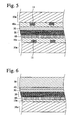
- the photoelectric conversion device of the present invention preferably has a lamination structure comprising an electrically conductive layer 10, an undercoating layer 60, a photosensitive layer 20 comprising fine semiconductor particles 21 sensitized by a dye 22 and an charge-transporting material 23 penetrating into voids among the fine semiconductor particles 21, a charge transfer layer 30, and a counter electrode layer 40 in this order.
- the charge-transporting material 23 is preferably the same as the electrolytic composition used in the charge transfer layer 30.
- the electrically conductive layer 10 and/or the counter electrode layer 40 may be supported by a substrate 50 to improve the strength of the photoelectric conversion device.
- a layer composed of the electrically conductive layer 10 and the substrate 50 optionally used for supporting it is referred to as "conductive support,” and a layer composed of the counter electrode layer 40 and the substrate 50 optionally used for supporting it is referred to as “counter electrode” hereinafter.
- the electrically conductive layer 10, the counter electrode layer 40 and the substrate 50 shown in Fig. 1 may be transparent.
- a light injected to the photosensitive layer 20 excites the dye 22, etc. to generate excited high-energy electrons, which are transported to a conduction band of the fine semiconductor particles 21, and are diffused to reach the electrically conductive layer 10.
- the dye 22 is in an oxidized form.
- electrons in the electrically conductive layer 10 return to the oxidized dye through the counter electrode layer 40 and the charge transfer layer 30 while doing job in an outside circuit, so that the dye 22 is regenerated.
- the photosensitive layer 20 generally acts as a negative electrode (photo-anode).
- the counter electrode layer 40 acts as a positive electrode.
- components of each layer may be diffused and mixed.
- the layers will be explained in detail below.
- the conductive support is: (1) a single layer of the electrically conductive layer, or (2) two layers of the electrically conductive layer and the substrate.
- the electrically conductive layer is preferably made of a material having such a strength that it can fully seal the photoelectric conversion device, for example, a metal such as platinum, gold, silver, copper, zinc, titanium, aluminum and an alloy thereof.
- a substrate having the electrically conductive layer containing an electrically conductive material formed on the photosensitive layer side may be used.
- the electrically conductive materials include metals such as platinum, gold, silver, copper, zinc, titanium, aluminum, indium and alloys thereof; carbon; electrically conductive metal oxides such as indium-tin composite oxides and tin oxides doped with fluorine or antimony; etc.
- the electrically conductive layer preferably has a thickness of 0.02 to 10 ⁇ m.
- the surface resistance of the conductive support is desirably as low as possible.
- the surface resistance of the conductive support is preferably 50 ⁇ /square or less, more preferably 20 ⁇ /square or less.
- the conductive support is substantially transparent.
- substantially transparent means that 10 % or more of light transmittance is obtained in part or all of a range from a visible light to a near infrared light (400-1200 nm).
- the light transmittance is preferably 50 % or more, more preferably 80 % or more.
- light transmittance is preferably high in a wavelength range in which the photosensitive layer has sensitivity.
- the transparent conductive support is preferably provided by forming the transparent electrically conductive layer comprising an electrically conductive metal oxide on the transparent substrate of such material as a glass and a plastic by coating or vapor deposition.
- the transparent electrically conductive layer is preferably made of tin dioxide doped with fluorine or antimony, or indium-tin oxide (ITO).
- the transparent substrate may be made of glass such as low-cost soda glass excellent in strength and a non-alkali glass suffering from no alkaline elution.
- a transparent polymer film may also be used as the transparent substrate.
- TAC triacetylcellulose
- PET polyethylene terephthalate
- PEN polyethylene naphthalate
- SPS syndiotactic polystyrene
- PPS polyphenylenesulfide
- PC polycarbonate
- PAr polyarylate
- PSF polysulfone
- PET polyimide
- PEI polyetherimide
- cyclic polyolefin a brominated phenoxy resin, etc.
- the amount of the electrically conductive metal oxide coated is preferably 0.01 to 100 g per 1 m 2 of the glass or plastic substrate.
- the metal lead is preferably made of a metal such as platinum, gold, nickel, titanium, aluminum, copper, silver, etc.
- the metal lead is preferably formed on the transparent substrate by a vapor deposition method, a sputtering method, etc., preferably with a transparent electrically conductive layer comprising conductive tin oxide or ITO formed thereon. Decrease in incident light quantity by the metal lead is suppressed to preferably 10 % or less, more preferably 1 to 5 %.
- the photosensitive layer comprises fine semiconductor particles sensitized by a dye.
- the fine semiconductor particles act as a photosensitive substance to absorb light and conduct charge separation, thereby generating electrons and positive holes.
- the light absorption and the generation of electrons and positive holes are primarily caused by the dye, and the fine semiconductor particles receive and convey electrons or positive holes.
- the semiconductor used in the present invention is preferably an n -type semiconductor, in which conductor electrons act as carriers under a photo-excitation condition to generate anode current.
- Used as the semiconductor may be simple semiconductor such as silicon and germanium; a III-V series compound semiconductor; a metal chalcogenide such as a metal oxide, a metal sulfide, a metal selenide and a composite thereof; a compound having a perovskite structure such as strontium titanate, calcium titanate, sodium titanate, barium titanate and potassium niobate; etc.
- the metal chalcogenide include oxides of titanium, tin, zinc, iron, tungsten, zirconium, hafnium, strontium, indium, cerium, yttrium, lanthanum, vanadium, niobium and tantalum; sulfides of cadmium, zinc, lead, silver, antimony and bismuth; selenides of cadmium or lead; cadmium telluride; etc.
- compound semiconductors such as phosphides of zinc, gallium, indium or cadmium, selenides of gallium-arsenic or copper-indium, copper-indium sulfide, etc. may be used in the present invention.
- composite semiconductors such as M x O y S z and M 1x M 2y O z are also preferably used in the present invention, wherein M, M 1 and M 2 independently represent a metal atom, O represents an oxygen atom, S represents a sulfur atom, and x, y and z represent numbers combined with each other to form a neutral molecule.
- the semiconductor are preferably Si, TiO 2 , SnO 2 , Fe 2 O 3 , WO 3 , ZnO, Nb 2 O 5 , CdS, ZnS, PbS, Bi 2 S 3 , CdSe, CdTe, SrTiO 3 , GaP, InP, GaAs, CuInS 2 and CuInSe 2 , more preferably TiO 2 , ZnO, SnO 2 , Fe 2 O 3 , WO 3 , Nb 2 O 5 , CdS, PbS, CdSe, SrTiO 3 , InP, GaAs, CuInS 2 and CuInSe 2 , further preferably TiO 2 and Nb 2 O 5 , and particularly TiO 2 .
- TiO 2 preferably contains 70% by volume or more, particularly 100% by volume, of an anatase-type crystal structure.
- the semiconductor is preferably doped with a metal to increase electron conductivity thereof. This metal is preferably divalent or trivalent. Further, the semiconductor is preferably doped with a monovalent metal to prevent a reverse current from the semiconductor to the charge transfer layer.
- the semiconductor used in the present invention may have a monocrystalline or polycrystalline structure. From the viewpoints of production cost, stable supply of raw materials, energy-payback time, etc., the semiconductor is preferably polycrystalline, particularly a porous layer of fine semiconductor particles.
- the photosensitive layer may partly contain an amorphous semiconductor.
- the particle size of the fine semiconductor particles is generally on the level of nm to ⁇ m.
- the average size of primary semiconductor particles which is determined by averaging the diameters of circles equivalent to projected areas thereof, is preferably 5 to 200 nm, more preferably 8 to 100 nm.
- the average size of secondary semiconductor particles in dispersion is preferably 0.01 to 30 ⁇ m.
- the average particle size of the smaller particles is preferably 25 nm or less, more preferably 10 nm or less.
- the fine semiconductor particles having a large particle size e.g. approximately 100 to 300 nm in diameter, may be used for the photosensitive layer.
- Two or more kinds of the fine semiconductor particles may be used in combination for the photosensitive layer.
- one is preferably TiO 2 , ZnO, Nb 2 O 5 or SrTiO 3 and the other is preferably SnO 2 , Fe 2 O 3 or WO 3 .
- More preferred combinations are ZnO and SnO 2 , ZnO and WO 3 , ZnO and SnO 2 and WO 3 , etc.
- When two or more fine semiconductor particles are combined their particle sizes may differ.
- Particularly preferred is a combination of larger-diameter particles of TiO 2 , ZnO, Nb 2 O 5 or SrTiO 3 and smaller-diameter particles of SnO 2 , Fe 2 O 3 or WO 3 .
- the larger-diameter particles are preferably 100 nm or more in an average size, while the smaller-diameter particles are preferably 15 nm or less in an average size.
- Preferably usable to produce the fine semiconductor particles are sol-gel methods described in Sumio Sakka, "Science of Sol-Gel Method,” issued by Agune Shofusha (1998 ), and “ Thin Film-Coating Technology by Sol-Gel Method” (1995) issued by the Technical Information Association , etc.; and gel-sol methods described in Tadao Sugimoto, "Synthesis of Mono-Dispersion Particles and Control of Their Size and Form by Novel Gel-Sol Method," and MATERIA, Vol. 35, No. 9, pages 1012 to 1018 (1996) .
- a method developed by Degussa which comprises preparing oxides by subjecting chlorides to a high-temperature hydrolysis in an oxyhydrogen salt.
- sol-gel methods In the case of using the fine semiconductor particles of TiO 2 , the above-described sol-gel methods, other sol-gel methods, and high-temperature hydrolysis methods in oxyhydrogen salts of chlorides are preferably used, and a sulfuric acid method and a chlorine method described in Manabu Seino, "Titanium oxide - Properties and Applied Technologies," issued by Gihodo Shuppan, (1997 ) may also be used. Further preferable as the sol-gel method are those described in Christophe J. Barb'e, et al, the Journal of American Ceramic Society, Vol. 80, No. 12, pages 3157 to 3171 (1997) , and Burnside, et al, Chemistry of Materials, Vol. 10, No. 9, pages 2419 to 2425 .
- the fine semiconductor particles may be applied onto the conductive support by a method for coating a conductive support with a dispersion or a colloidal solution containing fine semiconductor particles, in addition to the above-mentioned sol-gel method.
- a wet-type film production method is relatively advantageous for the mass production of the photoelectric conversion device, the properties of a liquid containing fine semiconductor particles, the feasibility of conductive supports, etc.
- Typical examples of such a wet-type film production method are a coating method, a printing method, an electrolytic deposition method and an electrodeposition method.
- the layer of fine semiconductor particles may be formed by a metal oxidation method, an LPD method for precipitating a metal from a metal solution by ligand exchange, a sputtering method, a vapor deposition method, a CVD method, or an SPD method for forming a metal oxide by thermally decomposing a metal oxide precursor sprayed onto a heated substrate.
- the dispersion containing fine semiconductor particles may be prepared by crushing the semiconductor in a mortar, by dispersing the semiconductor while grinding in a mill, or by synthesizing and precipitating the fine semiconductor particles in a reaction solvent, etc. in addition to the above-mentioned sol-gel method.
- dispersion solvents are water or organic solvents such as methanol, ethanol, isopropyl alcohol, citronellol, terpineol, dichloromethane, acetone, acetonitrile, ethyl acetate, etc.
- a Polymer such as polyethylene glycol, hydroxyethylcellulose and carboxymethylcellulose, a surfactant, an acid, a chelating agent, etc. may be used as a dispersing agent, if necessary.
- Polyethylene glycol is preferably added to the dispersion, because changing the molecular weight of the polyethylene glycol makes it possible to control the viscosity of the dispersion and the porosity of the resultant layer of fine semiconductor particles, and form a layer of fine semiconductor particles resistant to peeling.
- Preferable coating methods include application methods such as a roller method and a dipping method, metering methods such as an air-knife method and a blade method, etc. Further, preferable as methods for applying and metering in the same portion are a wire-bar method disclosed in JP 58-4589 B , a slide-hopper method described in U. S. Patents 2,681,294 , 2,761,419 and 2,761,791 , an extrusion method, a curtain method, etc. Further preferable as commonly usable methods are a spin method and a spray method.
- wet printing methods are three major printing methods by relief printing, offset printing and gravure printing, as well as an intaglio printing method, a gum printing method, a screen printing method, etc.
- a film production method may be selected from these methods depending on the viscosity of the dispersion and the desired wet thickness.
- the layer of fine semiconductor particles is not limited to a single layer. Dispersions comprising fine semiconductor particles having different particle sizes may be coated to form a multi-layer. Alternatively, dispersions containing different fine semiconductor particles, binders or additives may be coated to form a multi-layer. The multi-layer coating is effective, when it is impossible to form a layer having a sufficient thickness by one coating step.
- the preferable thickness of the layer of fine semiconductor particles is 0.1 to 100 ⁇ m.
- the thickness of the layer of fine semiconductor particles is preferably 1 to 30 ⁇ m, more preferably 2 to 25 ⁇ m.
- the amount of the fine semiconductor particles applied to the substrate is preferably 0.5 to 100 g, more preferably 3 to 50 g, per 1 m 2 of the substrate.
- the particles are preferably subjected to a heat treatment, thereby bringing them into electronic contact with each other, and increasing the strength of the resultant coating and their adhesion to the support.
- the heating temperature is preferably 40 to 700°C, more preferably 100 to 600°C.
- the heating time is preferably 10 minutes to 10 hours.
- High-temperature treatment is not preferable to a substrate having low melting point or softening point, such as a polymer film substrate, because it tends to deteriorate such a substrate.
- the heat treatment is preferably carried out at as low a temperature as possible, for example, 50 to 350°C, from the viewpoint of cost.
- Such a low-temperature heat treatment can be made possible by using a layer containing as fine semiconductor particles as 5 nm or less in average size, a mineral acid, a metal oxide precursor, etc. Further, the heat treatment may be carried out while applying an ultraviolet ray, an infrared ray, a microwave, an electric field, an ultrasonic wave, etc. to the fine semiconductor particles, to lower the heating temperature. To remove unnecessary organic compounds, etc., the heat treatment is preferably carried out in combination with evacuation, an oxygen plasma treatment, and washing with pure water, a solvent or a gas, etc.
- the layer of fine semiconductor particles may be subjected to chemical metal plating using an aqueous titanium tetrachloride solution, etc. or electrochemical metal plating using an aqueous titanium trichloride solution, etc., to increase the surface area and purity of the fine semiconductor particles, thereby improving the efficiency of injecting electrons into the particles from the dye. Further, to prevent reverse current from the fine semiconductor particles to the charge transfer layer, it is effective for the fine semiconductor particles to adsorb other low-electron conductivity organic compounds than the dye.
- the organic compound adsorbed preferably has a hydrophobic group.
- the layer of fine semiconductor particles preferably has a large surface area to adsorb a large amount of dye.
- the layer of fine semiconductor particles coated onto the substrate has a surface area of preferably 10 times or more, more preferably 100 times or more, as its projected area.
- the upper limit of the surface area is generally about 1000 times, though it is not particularly limited.
- any compound capable of absorbing visible and near infrared rays to sensitize the semiconductor may be used as the dye for the photosensitive layer
- preferable examples of such dyes include metal complex dyes, methine dyes, porphyrin-type dyes and phthalocyanine dyes.
- Two or more kinds of dyes may be used in combination to obtain a large photoelectric conversion wavelength region and high photoelectric conversion efficiency.
- the kinds and mixing ratios of the dyes may be determined depending on the wavelength region and strength distribution of the light source.
- the dye preferably has an appropriate interlocking group for interacting with the surfaces of the fine semiconductor particles.
- Preferred interlocking groups include acidic groups such as -COOH, -OH, -SO 3 H, -P(O)(OH) 2 and -OP(O)(OH) 2 , and ⁇ -conductive chelating groups such as oxime, dioxime, hydroxyquinoline, salicylate and ⁇ -ketoenolate groups. Particularly preferable among them are -COOH, -P(O)(OH) 2 and -OP(O)(OH) 2 .
- the interlocking group may form a salt with an alkali metal, etc. or an intramolecular salt.
- the preferred dyes for the photosensitive layer are specifically described below.
- the dye is a metal complex dye
- the dye is preferably a metallophthalocyanine dye, a metalloporphyrin dye or a ruthenium complex dye, particularly a ruthenium complex dye.
- the ruthenium complex dyes described in United States Patents 4,927,721 , 4,684,537 , 5,084,365 , 5,350,644 , 5,463,057 and 5,525,440 , JP 7-249790 A , JP 10-504512 A and JP 2000-26487 A , WO 98/50393 , etc. may be used in the present invention.
- the ruthenium complex dye is preferably represented by the following formula (IV): (A 1 ) p Ru(B-a)(B-b)(B-c) (IV), wherein A 1 represents a unidentate of SCN; p is an integer of 2; and B-a and B-b without B-c are the same organic ligands represented by the following formula B-1.
- the dye may be adsorbed to the fine semiconductor particles by soaking the conductive support having the well-dried layer of fine semiconductor particles in a dye solution, or by coating the dye solution to the layer of fine semiconductor particles.
- a soaking method, a dipping method, a roller-coating method, an air-knife method, etc. may be used.
- the dye may be adsorbed at a room temperature or while refluxing as described in JP 7-249790 A .
- a coating method of the latter a wire-bar method, a slide-hopper method, an extrusion method, a curtain method, a spin-coating method, a spraying method, etc. may be used.
- solvents for dissolving the dye include alcohols such as methanol, ethanol, t -butanol and benzyl alcohol; nitriles such as acetonitrile, propionitrile and 3-methoxypropionitrile; nitromethane; halogenated hydrocarbons such as dichloromethane, dichloroethane, chloroform and chlorobenzene; ethers such as diethylether and tetrahydrofuran; dimethylsulfoxide; amides such as N , N -dimethylformamide and N , N -dimethylacetamide; N -methylpyrrolidone; 1,3-dimethylimidazolidinone; 3-methyloxazolidinone; esters such as ethyl acetate and butyl acetate; carbonates such as diethyl carbonate, ethylene carbonate and propylene carbonate; ketones such as acetone, 2-butanone and cyclohex
- the total amount of the dye adsorbed is preferably 0.01 to 100 mmol per a unit surface area (1 m 2 ) of the layer of fine semiconductor particles.
- the amount of the dye adsorbed onto the fine semiconductor particles is preferably 0.01 to 1 mmol per 1 g of the fine semiconductor particles. With this adsorption amount of the dye, the semiconductor can be sufficiently sensitized. Too small an amount of the dye results in insufficient sensitization. On the other hand, if the amount of the dye is excessive, the dye not adsorbed onto the fine semiconductor particles is free, thereby reducing the sensitization of the fine semiconductor particles.
- the layer of fine semiconductor particles is subjected to a heat treatment before the dye is adsorbed thereonto. After the heat treatment, it is preferable for the layer of fine semiconductor particles to quickly adsorb the dye while it is still at 60 to 150°C without returning to room temperature, to prevent water from being adsorbed onto the layer of fine semiconductor particles.
- a colorless compound may be co-adsorbed onto the fine semiconductor particles together with the dye.
- the colorless compound preferably has surface activity, and examples thereof include steroid compounds having a carboxyl group such as chenodeoxycholic acid and sulfonates shown below.
- the dye not adsorbed on the layer of fine semiconductor particles is preferably removed by washing immediately after the dye adsorption process.
- the washing is preferably carried out by a wet-type washing bath with a polar solvent such as acetonitrile or an organic solvent such as alcohol.
- the surfaces of the fine semiconductor particles may be treated with an amine compound or a quaternary salt thereof after the dye adsorption process.
- the amine compound is preferably pyridine, 4- t -butylpyridine, polyvinylpyridine, etc.
- the quaternary salt is preferably tetrabutylammonium iodide, tetrahexylammonium iodide, etc.
- the amine compound or the quaternary salt may be used alone if it is liquid, or may be used in the form of a solution in an organic solvent.
- the charge transfer layer comprises the electrolytic composition of the present invention described above.
- the charge transfer layer may be formed by any of the following two methods. One method is to attach a counter electrode to a photosensitive layer beforehand and cause a material for a charge transfer layer in a liquid state to penetrate into a gap therebetween. Another method is to directly form a charge transfer layer on a photosensitive layer, and then form a counter electrode thereon.
- the charge transfer material may be caused to penetrate into the gap by a normal pressure process utilizing capillarity, or by a reduced pressure process where the material is sucked into the gap to replace a gas phase therein with a liquid phase.
- a counter electrode is attached while the charge transfer layer is still wet, to prevent the leakage of a liquid in edge portions.
- a gel electrolyte it is applied in a wet state and solidified by polymerization.
- the counter electrode may be attached after drying and solidification.
- a method for applying a wet organic hole-transporting material and a gel electrolyte apart from the electrolyte solution the same methods as those described above for forming a layer of fine semiconductor particles and applying a dye may be used.
- the charge transfer layer may be formed by a dry film-forming method such as a vacuum deposition method and a CVD method, followed by attaching a counter electrode thereto.
- the organic hole-transporting material may be introduced into the photosensitive layer by a vacuum deposition method, a casting method, a coating method, a spin-coating method, a soaking method, an electrolytic polymerization method, a photo-polymerization method, etc.
- the inorganic hole-transporting material may be introduced into the photosensitive layer by a casting method, a coating method, a spin-coating method, a soaking method, an electrolytic deposition method, an electroless deposition method, etc.
- the water content of the charge transfer layer is preferably 10,000 ppm or less, more preferably 2,000 ppm or less, and particularly 100 ppm or less.
- the counter electrode may be an electrically conductive layer alone or a laminate of the electrically conductive layer and the substrate.
- electrically conductive materials used for the counter electrode include metals such as platinum, gold, silver, copper, aluminum, magnesium and indium; carbon; and electrically conductive metal oxides such as indium-tin composite oxides and fluorine-doped tin oxides. Preferable among them are platinum, gold, silver, copper, aluminum and magnesium.
- the substrate for the counter electrode is preferably a glass or plastic plate, to which the above electrically conductive material is applied by coating or vapor deposition.
- the counter electrode layer preferably has a thickness of 3 nm to 10 ⁇ m, although the thickness is not particularly limited.
- the surface resistance of the counter electrode layer is desirably as low as possible. The surface resistance is preferably 50 ⁇ /square or less, more preferably 20 ⁇ /square or less.
- the conductive support is substantially transparent to permit light to pass therethrough.
- the counter electrode is preferably reflective to light.
- Such a counter electrode may be a glass or plastic plate vapor-deposited with a metal or an electrically conductive oxide, or a thin metal film.
- the counter electrode may be formed by coating, plating or vapor-deposition (PVD, CVD, etc.) of an electrically conductive material directly onto the charge transfer layer, or by attaching the electrically conductive layer formed on the substrate to the charge transfer layer.
- PVD vapor-deposition
- CVD vapor-deposition
- Preferable materials and forming methods of the metal lead, decrease in incident light quantity, etc. are the same as those in the conductive support.
- a thin, dense semiconductor film is preferably preformed as an undercoating layer between the conductive support and the photosensitive layer, to prevent short-circuiting between the counter electrode and the conductive support.
- the prevention of short-circuiting by this undercoating layer is effective particularly in the case of the charge transfer layer comprising the electron-transporting material or the hole-transporting material.
- the undercoating layer is made of TiO 2 , SnO 2 , Fe 2 O 3 , WO 3 , ZnO or Nb 2 O 5 , more preferably TiO 2 .
- the undercoating layer may be formed by a spray-pyrolysis method described in Electrochim. Acta, 40, 643 to 652 (1995) , a sputtering method, etc.
- the thickness of the undercoating layer is preferably 5 to 1000 nm, more preferably 10 to 500 nm.
- Functional layers such as a protective layer and a reflection-preventing layer may be formed on either one or both of the conductive support and the counter electrode acting as electrodes, between the electrically conductive layer and the substrate, or in the substrate.
- the functional layers may be formed by a coating method, a vapor deposition method, an attaching method, etc. depending on their materials.
- the photoelectric conversion device may have various interior structures depending on its use. It is classified into two major structures, one allowing light incidence from both faces, and another allowing it from only one side.
- Figs. 2 to 9 illustrate the interior structures of the photoelectric conversion device, to which the present invention is preferably applicable.
- a photosensitive layer 20 and a charge transfer layer 30 are formed between an electrically conductive, transparent layer 10a and a transparent counter electrode layer 40a. This structure allows light incidence from both sides of the device.
- a transparent substrate 50a partially having a metal lead 11 is provided with an electrically conductive, transparent layer 10a, an undercoating layer 60, a photosensitive layer 20, a charge transfer layer 30 and a counter electrode layer 40 in this order, and further provided with a substrate 50 thereon.
- This structure allows light incidence from the side of the electrically conductive layer.
- a substrate 50 having an electrically conductive layer 10 is provided with a photosensitive layer 20 via an undercoating layer 60, and then provided with a charge transfer layer 30 and a transparent counter electrode layer 40a thereon, and further provided with a transparent substrate 50a locally having a metal lead 11 inside.
- This structure allows light incidence from the side of the counter electrode.
- two transparent substrates 50a each partially having a metal lead 11 are provided with an electrically conductive transparent layer 10a or 40a, and then provided with an undercoating layer 60, a photosensitive layer 20 and a charge transfer layer 30 between the conductive layers.
- This structure allows light incidence from both sides of the photoelectric conversion device.
- a transparent substrate 50a is provided with an electrically conductive transparent layer 10a, an undercoating layer 60, a photosensitive layer 20, a charge transfer layer 30 and a counter electrode layer 40 in this order, and then attached to a substrate 50.
- This structure allows light incidence from the side of the electrically conductive layer.
- a substrate 50 is provided with an electrically conductive layer 10, an undercoating layer 60, a photosensitive layer 20, a charge transfer layer 30 and a transparent counter electrode layer 40a in this order, and then attached to a transparent substrate 50a.
- This structure allows light incidence from the side of the counter electrode.
- a transparent substrate 50a is provided with an electrically conductive transparent layer 10a, an undercoating layer 60, a photosensitive layer 20, a charge transfer layer 30 and a transparent counter electrode layer 40a in this order, and then attached to a transparent substrate 50a.
- This structure allows light incidence from both sides of the photoelectric conversion device.
- a substrate 50 is provided with an electrically conductive layer 10, an undercoating layer 60, a photosensitive layer 20, a solid charge transfer layer 30 in this order, and then partially provided with a counter electrode layer 40 or a metal lead 11. This structure allows light incidence from the side of the counter electrode.
- the photoelectric cell of the present invention comprises the above photoelectric conversion device of the present invention to do job in an external circuit.
- a photoelectric cell that has the charge transfer layer comprising the ion-conductive electrolytic composition is generally referred to as a photo-electrochemical cell.
- the photoelectric cell intended for generating power with solar light is referred to as a solar cell.
- edges of the photoelectric cell are preferably sealed with a polymer or an adhesive, etc. to prevent the cell content from deteriorating and evaporating.
- a known external circuit may be connected to the conductive support and the counter electrode via a lead.
- the interior structure of the solar cell may be essentially the same as that of the photoelectric conversion device mentioned above.
- the dye-sensitized solar cell comprising the photoelectric conversion device of the present invention may substantially have the same module structure as a conventional solar cell module.
- a cell is disposed on a substrate of metal, ceramic, etc. and covered with a packing resin, a protective glass, etc., whereby light is introduced from the opposite side of the substrate.
- the solar cell module may have a structure where the cell is placed on a substrate of a transparent material such as a tempered glass to introduce light from the transparent substrate side.
- a superstraight-type module structure, a substrate-type module structure, a potting-type module structure, substrate-integrated module structure that is generally used in amorphous silicon solar cells, etc. are known as the solar cell module structure.
- the dye-sensitive solar cell of the present invention may have a module structure properly selected from the above structures depending on ends, locations and environment where it is used, and preferably has a module structure disclosed in JP 2000-268892 A .
- electrolyte salts used in the electrolytic compositions were synthesized as follows. The structure of each electrolyte salt was identified by NMR and Mass spectrum.
- the resultant residue was purified by a silica gel column (eluent: methanol/dichloromethane) to obtain 3.0 g of an electrolyte salt D-18.
- the mass spectrum of the electrolyte salt D-18 revealed that it had a mass (POSI) of 334.
- the above titanium dioxide dispersion was applied to an electrically conductive glass having a fluorine-doped tin oxide layer (20 mm x 20 mm, "TCO Glass-U" available from Asahi Glass K. K. with a surface resistance of approximately 30 ⁇ /square) on its conductive surface by a glass bar.
- the amount of the fine semiconductor particles coated was 20 g/m 2 .
- eight conductive glasses were arranged such that the adhesive tapes were positioned at both ends, to coat them with the titanium dioxide dispersion simultaneously. After peeling the adhesive tapes, the coated conductive glasses were air-dried at room temperature for a day.
- Each coated conductive glass was then placed in an electric furnace (muffle furnace "FP-32" available from Yamato Science K. K.), and calcined at 450°C for 30 minutes to obtain a TiO 2 electrode.
- the electrode was immersed in a solution of Dye R-1 in ethanol (3 x 10 -4 mol/l) for 3 hours and then in 4- t -butylpyridine for 15 minutes. It was then washed with acetonitrile and spontaneously dried to obtain a dye-sensitized TiO 2 electrode substrate.
- the above dye-sensitized TiO 2 electrode substrate (20 mm x 20 mm) was laminated on a platinum-vapor-deposited glass having the same size.
- an electrolytic composition comprising 98% by mass of the following electrolyte salt Y-1 and 2% by mass of iodine was permeated into the TiO 2 electrode in a gap between the two glasses by capillarity, and sealed with an epoxy-based sealant to obtain a photoelectric conversion device of Comparative Example 1.
- the photoelectric conversion devices of Examples 1 to 11 each comprising the electrolyte salt (I) were superior in photoelectric conversion efficiency to those of Comparative Examples 1 to 5 each comprising a conventional electrolyte salt.
- the electrolytic composition suitable for a dye-sensitized solar cell of the present invention is excellent in charge-transporting capability.
- the photoelectric conversion device comprising this electrolytic composition exhibits excellent photoelectric conversion properties.
- the photoelectric cell comprising such photoelectric conversion device is remarkably useful as a solar cell.
Landscapes
- Chemical & Material Sciences (AREA)
- Organic Chemistry (AREA)
- Chemical Kinetics & Catalysis (AREA)
- Electrochemistry (AREA)
- Engineering & Computer Science (AREA)
- Power Engineering (AREA)
- Microelectronics & Electronic Packaging (AREA)
- General Chemical & Material Sciences (AREA)
- Photovoltaic Devices (AREA)
- Hybrid Cells (AREA)
- Conductive Materials (AREA)
Claims (4)
- Farbstoff-sensibilisierte Solarzelle, umfassend eine photoelektrische Umwandlungsvorrichtung, umfassend einen leitfähigen Träger, eine lichtempfindliche Schicht (20), eine Ladungsübertragungsschicht (30) und eine Gegenelektrode (40), wobei
der leitfähige Träger ein leitfähiges Glas umfasst,
die lichtempfindliche Schicht (20) feine Halbleiterteilchen (21) aus mit einem Farbstoff (22) sensibilisiertem TiO2 umfasst,
die Gegenelektrode (40) die gleiche ist, wie das leitfähige Glas im leitfähigen Träger,
dadurch gekennzeichnet, dass
die Ladungsübertragungsschicht (30) eine Elektrolytzusammensetzung umfasst, umfassend ein Elektrolytsalz der allgemeinen Formel (I):
(Q1)n1(X)n2 (I),
wobei Q1 ein unsubstituiertes Imidazolium Kation bedeutet, X ein Anion mit einem Siliziumatom bedeutet, n1 und n2 jeweils eine ganze Zahl von 1 bedeuten, wobei X repräsentiert wird durch die nachstehende allgemeine Formel II:
- Farbstoff-sensibilisierte Solarzelle nach Anspruch 1, wobei das leitfähige Glas ein mit Platin bedampftes Glas ist.
- Farbstoff-sensibilisierte Solarzelle nach Anspruch 1, wobei der Farbstoff (22) ein Ruthenium-Komplexfarbstoff der nachstehenden Formel (IV) ist:
(A1)pRu(B-a)(B-b)(B-c (IV),
wobei A1 für SCN steht; p eine ganze Zahl von 2 ist; und B-a und B-b ohne B-c die gleichen organischen Liganden sind, repräsentiert durch die nachstehende Formel B-1.
- Verbindung gemäß der nachstehenden allgemeinen Formel (III):

Applications Claiming Priority (2)
| Application Number | Priority Date | Filing Date | Title |
|---|---|---|---|
| JP2001283172 | 2001-09-18 | ||
| JP2001283172A JP2003092153A (ja) | 2001-09-18 | 2001-09-18 | 電解質組成物、光電変換素子及び光電池 |
Publications (3)
| Publication Number | Publication Date |
|---|---|
| EP1293997A2 EP1293997A2 (de) | 2003-03-19 |
| EP1293997A3 EP1293997A3 (de) | 2006-06-07 |
| EP1293997B1 true EP1293997B1 (de) | 2008-05-28 |
Family
ID=19106708
Family Applications (1)
| Application Number | Title | Priority Date | Filing Date |
|---|---|---|---|
| EP02019739A Expired - Lifetime EP1293997B1 (de) | 2001-09-18 | 2002-09-03 | Imidazolverbindungen und Elektrolytzusammensetzung für eine Farbstoffsolarzelle |
Country Status (4)
| Country | Link |
|---|---|
| EP (1) | EP1293997B1 (de) |
| JP (1) | JP2003092153A (de) |
| AT (1) | ATE397279T1 (de) |
| DE (1) | DE60226822D1 (de) |
Families Citing this family (15)
| Publication number | Priority date | Publication date | Assignee | Title |
|---|---|---|---|---|
| GB0319799D0 (en) * | 2003-08-22 | 2003-09-24 | Itm Power Ltd | Photovoltaic cell |
| KR101056440B1 (ko) * | 2003-09-26 | 2011-08-11 | 삼성에스디아이 주식회사 | 염료감응 태양전지 |
| JP4655519B2 (ja) * | 2004-06-18 | 2011-03-23 | 株式会社ブリヂストン | 色素増感型太陽電池用電解液及び色素増感型太陽電池 |
| US7943849B2 (en) * | 2007-03-30 | 2011-05-17 | Tdk Corporation | Photoelectric conversion device |
| WO2010050575A1 (ja) | 2008-10-29 | 2010-05-06 | 富士フイルム株式会社 | 色素、これを用いた光電変換素子、光電気化学電池、および色素の製造方法 |
| FR2943260B1 (fr) * | 2009-03-23 | 2012-05-04 | Univ Savoie | Utilisation de sels organiques a anion halogenure pour pieger l'ozone |
| JP5350851B2 (ja) * | 2009-03-26 | 2013-11-27 | 日本化学工業株式会社 | 光電変換素子用組成物及びそれを用いた光電変換素子 |
| JP5524557B2 (ja) | 2009-09-28 | 2014-06-18 | 富士フイルム株式会社 | 光電変換素子の製造方法、光電変換素子、および光電気化学電池 |
| JP5620081B2 (ja) | 2009-09-28 | 2014-11-05 | 富士フイルム株式会社 | 光電変換素子の製造方法 |
| JP5583990B2 (ja) | 2010-02-26 | 2014-09-03 | 株式会社Adeka | 光電変換素子及び光電変換素子用色素 |
| JP5972811B2 (ja) | 2013-02-22 | 2016-08-17 | 富士フイルム株式会社 | 光電変換素子、光電変換素子の製造方法および色素増感太陽電池 |
| CN110710046B (zh) * | 2017-06-01 | 2022-11-08 | 昭和电工材料株式会社 | 电解液和电化学装置 |
| KR102130029B1 (ko) * | 2018-03-16 | 2020-07-03 | 삼성에스디아이 주식회사 | 리튬 이차 전지용 전해액 및 이를 포함하는 리튬 이차 전지 |
| JP7158335B2 (ja) * | 2018-06-25 | 2022-10-21 | 信越化学工業株式会社 | 生体電極組成物、生体電極、及び生体電極の製造方法 |
| WO2023069051A1 (en) * | 2021-10-21 | 2023-04-27 | Sabanci Üni̇versi̇tesi̇ Nanoteknoloji̇ Araştirma Ve Uygulama Merkezi̇ | Gel electrolyte for use in an energy storage device and supercapacitor cell |
Family Cites Families (3)
| Publication number | Priority date | Publication date | Assignee | Title |
|---|---|---|---|---|
| DE69416428T2 (de) * | 1993-12-29 | 1999-09-16 | Ecole Polytech | Photoelektrochemische zelle und elektrolyt für diese zelle |
| KR20010086196A (ko) * | 1997-09-11 | 2001-09-10 | 추후보정 | 폴리플루오로알콕사이드 리간드를 함유한 약한 배위결합음이온 |
| WO1999028292A1 (fr) * | 1997-12-01 | 1999-06-10 | Acep Inc. | Sels de sulfones perfluores, et leurs utilisations comme materiaux a conduction ionique |
-
2001
- 2001-09-18 JP JP2001283172A patent/JP2003092153A/ja active Pending
-
2002
- 2002-09-03 EP EP02019739A patent/EP1293997B1/de not_active Expired - Lifetime
- 2002-09-03 AT AT02019739T patent/ATE397279T1/de not_active IP Right Cessation
- 2002-09-03 DE DE60226822T patent/DE60226822D1/de not_active Expired - Lifetime
Also Published As
| Publication number | Publication date |
|---|---|
| EP1293997A3 (de) | 2006-06-07 |
| EP1293997A2 (de) | 2003-03-19 |
| JP2003092153A (ja) | 2003-03-28 |
| ATE397279T1 (de) | 2008-06-15 |
| DE60226822D1 (de) | 2008-07-10 |
Similar Documents
| Publication | Publication Date | Title |
|---|---|---|
| EP1180774B1 (de) | Photoelektrische Zelle und Herstellungsmethode | |
| EP1176618B1 (de) | Ruthenium-Komplexfarbstoff, photoelektrische Umwandlungsvorrichtung und photoelektrische Zelle | |
| EP1075005A2 (de) | Elektrolytzusammensetzung und photolektrochemische Zelle | |
| US8124869B2 (en) | Dye-sensitized type solar cell | |
| EP1083582B1 (de) | Farbstoffsensiblisierte photoelektrochemische Zelle | |
| EP1293997B1 (de) | Imidazolverbindungen und Elektrolytzusammensetzung für eine Farbstoffsolarzelle | |
| EP1089305B1 (de) | Elektrolyt-Zusammensetzung, photoelektrische Umwandlungsvorrichtung und photoelektrochemische Zelle | |
| JP2003187881A (ja) | 光電変換素子の作製方法、光電変換素子及び光電池 | |
| EP1341196B9 (de) | Elektrolytzusammensetzung, Vorrichtung zur photoelektrischen Umwandlung und photoelektrische Zelle | |
| EP1213776A2 (de) | Metallkomplex-Farbstoff für eine farbstoffsensibilisierte Solarzelle | |
| EP1375428B1 (de) | Verfahren zur Herstellung von titandioxidsolen und feine titandioxid-Partikel, sowie Verwendung in photoelektrischen Halbleiter-Umwandlungsvorrichtungen | |
| EP1164603A2 (de) | Farbstoffsensibilisierte Solarzelle | |
| EP1271581B1 (de) | Elektrolytezusammensetzung, photoelektrische Umwandlungsvorrichtung und photoelektrochemische Zelle | |
| EP1296339A2 (de) | Herstellungsmethode für eine photoelektrochemische Zelle | |
| JP2003017148A (ja) | 電解質組成物、光電変換素子及び光電気化学電池 | |
| EP1231619A2 (de) | Metallkomplex-Farbstoff für eine photoelektrochemische Zelle | |
| JP4278079B2 (ja) | 高感度受光素子及び光センサー | |
| JP2003217693A (ja) | 半導体微粒子層、光電変換素子及び光電池 | |
| JP4072891B2 (ja) | 光電変換素子の作製方法及び光電池 | |
| JP4958331B2 (ja) | 光電変換素子の製造方法、光電変換素子および光電池 | |
| JP4776871B2 (ja) | 半導体微粒子膜、光電変換素子及び光電池 | |
| JP2002246620A (ja) | 光電変換素子および光電池とその作成方法 | |
| JP2004238213A (ja) | 酸化チタン粒子の製造方法、及びそれを用いた光電変換素子 | |
| JP4937438B2 (ja) | 光電変換用半導体、光電変換素子および光電池 | |
| JP2003187882A (ja) | 光電変換素子の作製方法、光電変換素子及び光電池 |
Legal Events
| Date | Code | Title | Description |
|---|---|---|---|
| PUAI | Public reference made under article 153(3) epc to a published international application that has entered the european phase |
Free format text: ORIGINAL CODE: 0009012 |
|
| AK | Designated contracting states |
Designated state(s): AT BE BG CH CY CZ DE DK EE ES FI FR GB GR IE IT LI LU MC NL PT SE SK TR Kind code of ref document: A2 Designated state(s): AT BE BG CH CY CZ DE DK EE ES FI FR GB GR IE IT LI LU MC NL PT SE SK TR |
|
| AX | Request for extension of the european patent |
Extension state: AL LT LV MK RO SI |
|
| PUAL | Search report despatched |
Free format text: ORIGINAL CODE: 0009013 |
|
| AK | Designated contracting states |
Kind code of ref document: A3 Designated state(s): AT BE BG CH CY CZ DE DK EE ES FI FR GB GR IE IT LI LU MC NL PT SE SK TR |
|
| AX | Request for extension of the european patent |
Extension state: AL LT LV MK RO SI |
|
| 17P | Request for examination filed |
Effective date: 20061023 |
|
| 17Q | First examination report despatched |
Effective date: 20061215 |
|
| AKX | Designation fees paid |
Designated state(s): AT BE BG CH CY CZ DE DK EE ES FI FR GB GR IE IT LI LU MC NL PT SE SK TR |
|
| RAP1 | Party data changed (applicant data changed or rights of an application transferred) |
Owner name: FUJIFILM CORPORATION |
|
| GRAP | Despatch of communication of intention to grant a patent |
Free format text: ORIGINAL CODE: EPIDOSNIGR1 |
|
| RTI1 | Title (correction) |
Free format text: IMIDAZOLIUM COMPOUNDS AND ELECTROLYTIC COMPOSITION FOR A DYE SENSITIZED SOLAR CELL |
|
| GRAS | Grant fee paid |
Free format text: ORIGINAL CODE: EPIDOSNIGR3 |
|
| GRAA | (expected) grant |
Free format text: ORIGINAL CODE: 0009210 |
|
| AK | Designated contracting states |
Kind code of ref document: B1 Designated state(s): AT BE BG CH CY CZ DE DK EE ES FI FR GB GR IE IT LI LU MC NL PT SE SK TR |
|
| REG | Reference to a national code |
Ref country code: GB Ref legal event code: FG4D |
|
| REG | Reference to a national code |
Ref country code: CH Ref legal event code: EP |
|
| REF | Corresponds to: |
Ref document number: 60226822 Country of ref document: DE Date of ref document: 20080710 Kind code of ref document: P |
|
| REG | Reference to a national code |
Ref country code: IE Ref legal event code: FG4D |
|
| PG25 | Lapsed in a contracting state [announced via postgrant information from national office to epo] |
Ref country code: ES Free format text: LAPSE BECAUSE OF FAILURE TO SUBMIT A TRANSLATION OF THE DESCRIPTION OR TO PAY THE FEE WITHIN THE PRESCRIBED TIME-LIMIT Effective date: 20080908 Ref country code: FI Free format text: LAPSE BECAUSE OF FAILURE TO SUBMIT A TRANSLATION OF THE DESCRIPTION OR TO PAY THE FEE WITHIN THE PRESCRIBED TIME-LIMIT Effective date: 20080528 |
|
| PG25 | Lapsed in a contracting state [announced via postgrant information from national office to epo] |
Ref country code: NL Free format text: LAPSE BECAUSE OF FAILURE TO SUBMIT A TRANSLATION OF THE DESCRIPTION OR TO PAY THE FEE WITHIN THE PRESCRIBED TIME-LIMIT Effective date: 20080528 Ref country code: AT Free format text: LAPSE BECAUSE OF FAILURE TO SUBMIT A TRANSLATION OF THE DESCRIPTION OR TO PAY THE FEE WITHIN THE PRESCRIBED TIME-LIMIT Effective date: 20080528 |
|
| NLV1 | Nl: lapsed or annulled due to failure to fulfill the requirements of art. 29p and 29m of the patents act | ||
| PG25 | Lapsed in a contracting state [announced via postgrant information from national office to epo] |
Ref country code: CZ Free format text: LAPSE BECAUSE OF FAILURE TO SUBMIT A TRANSLATION OF THE DESCRIPTION OR TO PAY THE FEE WITHIN THE PRESCRIBED TIME-LIMIT Effective date: 20080528 Ref country code: DK Free format text: LAPSE BECAUSE OF FAILURE TO SUBMIT A TRANSLATION OF THE DESCRIPTION OR TO PAY THE FEE WITHIN THE PRESCRIBED TIME-LIMIT Effective date: 20080528 Ref country code: SE Free format text: LAPSE BECAUSE OF FAILURE TO SUBMIT A TRANSLATION OF THE DESCRIPTION OR TO PAY THE FEE WITHIN THE PRESCRIBED TIME-LIMIT Effective date: 20080828 Ref country code: PT Free format text: LAPSE BECAUSE OF FAILURE TO SUBMIT A TRANSLATION OF THE DESCRIPTION OR TO PAY THE FEE WITHIN THE PRESCRIBED TIME-LIMIT Effective date: 20081028 |
|
| PG25 | Lapsed in a contracting state [announced via postgrant information from national office to epo] |
Ref country code: SK Free format text: LAPSE BECAUSE OF FAILURE TO SUBMIT A TRANSLATION OF THE DESCRIPTION OR TO PAY THE FEE WITHIN THE PRESCRIBED TIME-LIMIT Effective date: 20080528 Ref country code: BE Free format text: LAPSE BECAUSE OF FAILURE TO SUBMIT A TRANSLATION OF THE DESCRIPTION OR TO PAY THE FEE WITHIN THE PRESCRIBED TIME-LIMIT Effective date: 20080528 |
|
| PLBE | No opposition filed within time limit |
Free format text: ORIGINAL CODE: 0009261 |
|
| STAA | Information on the status of an ep patent application or granted ep patent |
Free format text: STATUS: NO OPPOSITION FILED WITHIN TIME LIMIT |
|
| PG25 | Lapsed in a contracting state [announced via postgrant information from national office to epo] |
Ref country code: EE Free format text: LAPSE BECAUSE OF FAILURE TO SUBMIT A TRANSLATION OF THE DESCRIPTION OR TO PAY THE FEE WITHIN THE PRESCRIBED TIME-LIMIT Effective date: 20080528 Ref country code: BG Free format text: LAPSE BECAUSE OF FAILURE TO SUBMIT A TRANSLATION OF THE DESCRIPTION OR TO PAY THE FEE WITHIN THE PRESCRIBED TIME-LIMIT Effective date: 20080828 Ref country code: MC Free format text: LAPSE BECAUSE OF NON-PAYMENT OF DUE FEES Effective date: 20080930 |
|
| REG | Reference to a national code |
Ref country code: CH Ref legal event code: PL |
|
| 26N | No opposition filed |
Effective date: 20090303 |
|
| GBPC | Gb: european patent ceased through non-payment of renewal fee |
Effective date: 20080903 |
|
| REG | Reference to a national code |
Ref country code: IE Ref legal event code: MM4A |
|
| REG | Reference to a national code |
Ref country code: FR Ref legal event code: ST Effective date: 20090529 |
|
| PG25 | Lapsed in a contracting state [announced via postgrant information from national office to epo] |
Ref country code: IE Free format text: LAPSE BECAUSE OF NON-PAYMENT OF DUE FEES Effective date: 20080903 |
|
| PG25 | Lapsed in a contracting state [announced via postgrant information from national office to epo] |
Ref country code: IT Free format text: LAPSE BECAUSE OF FAILURE TO SUBMIT A TRANSLATION OF THE DESCRIPTION OR TO PAY THE FEE WITHIN THE PRESCRIBED TIME-LIMIT Effective date: 20080528 |
|
| PG25 | Lapsed in a contracting state [announced via postgrant information from national office to epo] |
Ref country code: LI Free format text: LAPSE BECAUSE OF NON-PAYMENT OF DUE FEES Effective date: 20080930 Ref country code: FR Free format text: LAPSE BECAUSE OF NON-PAYMENT OF DUE FEES Effective date: 20080930 Ref country code: CH Free format text: LAPSE BECAUSE OF NON-PAYMENT OF DUE FEES Effective date: 20080930 |
|
| PG25 | Lapsed in a contracting state [announced via postgrant information from national office to epo] |
Ref country code: GB Free format text: LAPSE BECAUSE OF NON-PAYMENT OF DUE FEES Effective date: 20080903 |
|
| PG25 | Lapsed in a contracting state [announced via postgrant information from national office to epo] |
Ref country code: LU Free format text: LAPSE BECAUSE OF NON-PAYMENT OF DUE FEES Effective date: 20080903 Ref country code: CY Free format text: LAPSE BECAUSE OF FAILURE TO SUBMIT A TRANSLATION OF THE DESCRIPTION OR TO PAY THE FEE WITHIN THE PRESCRIBED TIME-LIMIT Effective date: 20080528 |
|
| PG25 | Lapsed in a contracting state [announced via postgrant information from national office to epo] |
Ref country code: TR Free format text: LAPSE BECAUSE OF FAILURE TO SUBMIT A TRANSLATION OF THE DESCRIPTION OR TO PAY THE FEE WITHIN THE PRESCRIBED TIME-LIMIT Effective date: 20080528 |
|
| PG25 | Lapsed in a contracting state [announced via postgrant information from national office to epo] |
Ref country code: GR Free format text: LAPSE BECAUSE OF FAILURE TO SUBMIT A TRANSLATION OF THE DESCRIPTION OR TO PAY THE FEE WITHIN THE PRESCRIBED TIME-LIMIT Effective date: 20080829 |
|
| PGFP | Annual fee paid to national office [announced via postgrant information from national office to epo] |
Ref country code: DE Payment date: 20150825 Year of fee payment: 14 |
|
| REG | Reference to a national code |
Ref country code: DE Ref legal event code: R119 Ref document number: 60226822 Country of ref document: DE |
|
| PG25 | Lapsed in a contracting state [announced via postgrant information from national office to epo] |
Ref country code: DE Free format text: LAPSE BECAUSE OF NON-PAYMENT OF DUE FEES Effective date: 20170401 |