EP1289356A1 - Method and device for drying materials and method of producing circuit boards using the same - Google Patents
Method and device for drying materials and method of producing circuit boards using the same Download PDFInfo
- Publication number
- EP1289356A1 EP1289356A1 EP01938558A EP01938558A EP1289356A1 EP 1289356 A1 EP1289356 A1 EP 1289356A1 EP 01938558 A EP01938558 A EP 01938558A EP 01938558 A EP01938558 A EP 01938558A EP 1289356 A1 EP1289356 A1 EP 1289356A1
- Authority
- EP
- European Patent Office
- Prior art keywords
- air
- circuit board
- board
- drying
- board material
- Prior art date
- Legal status (The legal status is an assumption and is not a legal conclusion. Google has not performed a legal analysis and makes no representation as to the accuracy of the status listed.)
- Withdrawn
Links
Images



Classifications
-
- H—ELECTRICITY
- H05—ELECTRIC TECHNIQUES NOT OTHERWISE PROVIDED FOR
- H05K—PRINTED CIRCUITS; CASINGS OR CONSTRUCTIONAL DETAILS OF ELECTRIC APPARATUS; MANUFACTURE OF ASSEMBLAGES OF ELECTRICAL COMPONENTS
- H05K3/00—Apparatus or processes for manufacturing printed circuits
- H05K3/40—Forming printed elements for providing electric connections to or between printed circuits
- H05K3/4038—Through-connections; Vertical interconnect access [VIA] connections
- H05K3/4053—Through-connections; Vertical interconnect access [VIA] connections by thick-film techniques
- H05K3/4069—Through-connections; Vertical interconnect access [VIA] connections by thick-film techniques for via connections in organic insulating substrates
-
- F—MECHANICAL ENGINEERING; LIGHTING; HEATING; WEAPONS; BLASTING
- F26—DRYING
- F26B—DRYING SOLID MATERIALS OR OBJECTS BY REMOVING LIQUID THEREFROM
- F26B5/00—Drying solid materials or objects by processes not involving the application of heat
- F26B5/04—Drying solid materials or objects by processes not involving the application of heat by evaporation or sublimation of moisture under reduced pressure, e.g. in a vacuum
-
- H—ELECTRICITY
- H05—ELECTRIC TECHNIQUES NOT OTHERWISE PROVIDED FOR
- H05K—PRINTED CIRCUITS; CASINGS OR CONSTRUCTIONAL DETAILS OF ELECTRIC APPARATUS; MANUFACTURE OF ASSEMBLAGES OF ELECTRICAL COMPONENTS
- H05K3/00—Apparatus or processes for manufacturing printed circuits
- H05K3/22—Secondary treatment of printed circuits
- H05K3/227—Drying of printed circuits
-
- H—ELECTRICITY
- H05—ELECTRIC TECHNIQUES NOT OTHERWISE PROVIDED FOR
- H05K—PRINTED CIRCUITS; CASINGS OR CONSTRUCTIONAL DETAILS OF ELECTRIC APPARATUS; MANUFACTURE OF ASSEMBLAGES OF ELECTRICAL COMPONENTS
- H05K2201/00—Indexing scheme relating to printed circuits covered by H05K1/00
- H05K2201/03—Conductive materials
- H05K2201/0332—Structure of the conductor
- H05K2201/0335—Layered conductors or foils
- H05K2201/0355—Metal foils
-
- H—ELECTRICITY
- H05—ELECTRIC TECHNIQUES NOT OTHERWISE PROVIDED FOR
- H05K—PRINTED CIRCUITS; CASINGS OR CONSTRUCTIONAL DETAILS OF ELECTRIC APPARATUS; MANUFACTURE OF ASSEMBLAGES OF ELECTRICAL COMPONENTS
- H05K2203/00—Indexing scheme relating to apparatus or processes for manufacturing printed circuits covered by H05K3/00
- H05K2203/01—Tools for processing; Objects used during processing
- H05K2203/0191—Using tape or non-metallic foil in a process, e.g. during filling of a hole with conductive paste
-
- H—ELECTRICITY
- H05—ELECTRIC TECHNIQUES NOT OTHERWISE PROVIDED FOR
- H05K—PRINTED CIRCUITS; CASINGS OR CONSTRUCTIONAL DETAILS OF ELECTRIC APPARATUS; MANUFACTURE OF ASSEMBLAGES OF ELECTRICAL COMPONENTS
- H05K2203/00—Indexing scheme relating to apparatus or processes for manufacturing printed circuits covered by H05K3/00
- H05K2203/08—Treatments involving gases
- H05K2203/081—Blowing of gas, e.g. for cooling or for providing heat during solder reflowing
-
- H—ELECTRICITY
- H05—ELECTRIC TECHNIQUES NOT OTHERWISE PROVIDED FOR
- H05K—PRINTED CIRCUITS; CASINGS OR CONSTRUCTIONAL DETAILS OF ELECTRIC APPARATUS; MANUFACTURE OF ASSEMBLAGES OF ELECTRICAL COMPONENTS
- H05K2203/00—Indexing scheme relating to apparatus or processes for manufacturing printed circuits covered by H05K3/00
- H05K2203/08—Treatments involving gases
- H05K2203/085—Using vacuum or low pressure
-
- H—ELECTRICITY
- H05—ELECTRIC TECHNIQUES NOT OTHERWISE PROVIDED FOR
- H05K—PRINTED CIRCUITS; CASINGS OR CONSTRUCTIONAL DETAILS OF ELECTRIC APPARATUS; MANUFACTURE OF ASSEMBLAGES OF ELECTRICAL COMPONENTS
- H05K2203/00—Indexing scheme relating to apparatus or processes for manufacturing printed circuits covered by H05K3/00
- H05K2203/14—Related to the order of processing steps
- H05K2203/1461—Applying or finishing the circuit pattern after another process, e.g. after filling of vias with conductive paste, after making printed resistors
-
- H—ELECTRICITY
- H05—ELECTRIC TECHNIQUES NOT OTHERWISE PROVIDED FOR
- H05K—PRINTED CIRCUITS; CASINGS OR CONSTRUCTIONAL DETAILS OF ELECTRIC APPARATUS; MANUFACTURE OF ASSEMBLAGES OF ELECTRICAL COMPONENTS
- H05K3/00—Apparatus or processes for manufacturing printed circuits
- H05K3/0011—Working of insulating substrates or insulating layers
- H05K3/0017—Etching of the substrate by chemical or physical means
- H05K3/0026—Etching of the substrate by chemical or physical means by laser ablation
- H05K3/0032—Etching of the substrate by chemical or physical means by laser ablation of organic insulating material
-
- H—ELECTRICITY
- H05—ELECTRIC TECHNIQUES NOT OTHERWISE PROVIDED FOR
- H05K—PRINTED CIRCUITS; CASINGS OR CONSTRUCTIONAL DETAILS OF ELECTRIC APPARATUS; MANUFACTURE OF ASSEMBLAGES OF ELECTRICAL COMPONENTS
- H05K3/00—Apparatus or processes for manufacturing printed circuits
- H05K3/0011—Working of insulating substrates or insulating layers
- H05K3/0055—After-treatment, e.g. cleaning or desmearing of holes
Definitions
- the present invention relates to a method and system of drying materials and a method of manufacturing circuit boards using the same.
- a double-sided or multi-layered circuit board is employed more frequently than a conventional single-sided board, as a circuit board on which electronic components are mounted, and a high density circuit board allowing a larger number of circuits to be integrated in a circuit board is developed.
- the substrate material is drilled together with a film bonded thereto and the film is used as a mask for filling the conductive paste into the fine holes. Therefore, all the substrate material including the film must be kept clean.
- both drilling and laser machining produce a large amount of cutting dusts, and the cutting dusts may adhere to the board material and close the holes for electrical connection. In addition, a little dust in air may close the fine holes.
- the board material is cleaned before the conductive paste is filled.
- new wet cleaning methods as ultrasonic cleaning are employed. These methods require drying after cleaning, in order to remove the moisture absorbed from the periphery of the machined holes or the outer ends of the board material.
- mask films 2a and 2b are bonded to substrate material 1.
- substrate material 1 Provided at an end of substrate material 1 are peel off leading parts 3a and 3b for stripping mask films 2a and 2b after the conductive paste is filled.
- the leading parts 3a and 3b are made by stripping a part of each of mask films 2a and 2b.
- a small number of sheets could be treated with a vacuum dryer. However, it takes long time to dry a large number of sheets because sufficient latent heat cannot be given to the material under vacuum and thus calories sufficient to remove the moisture cannot be added.
- the conventional method is not efficient and may possess problems e.g. causing more damage to the board material.
- the present invention is directed to realize a board material having high-quality fine holes and to provide a method and a system of manufacturing highly reliable circuit boards at low cost.
- a method of manufacturing circuit boards in accordance with the present invention includes a bonding step of bonding a film-like material to at least one side of a board material to form a substrate material having a film(s).
- the method of manufacturing a circuit boards also includes: a hole-forming step of drilling a through or a blind hole in the board material made of a plurality of materials; and a step of forming a connection means in the through or blind hole for mutually connecting circuits formed on or in the circuit board.
- the hole-forming step includes: a step of irradiating the board material with laser to form a through or blind hole shape; and a step of cleaning to remove foreign substances that have attached to the surface of the board material and the inner wall of the through or blind hole in the previous step.
- the method can provide a clean and highly reliable board material by efficiently drying the moisture absorbed by the board material, without damaging the board material, after the removal of water drops that have adhered to the surface of the board material in a cleaning process.
- Figs. 1 (a) to (h) shows cross sectional views of a process of a method of manufacturing a multi-layered circuit board in accordance with the present embodiment.
- reference numeral 1 shows a substrate material that is a square plate of 250 mm on each side and approx. 150 ⁇ m thick, as an insulating substrate.
- a resin impregnated substrate made of a composite material in which an non-woven fabric made of an aromatic polyamide fiber (hereinafter referred to as “aramid fiber”) is impregnated with a thermosetting epoxy resin (hereinafter referred to as "epoxy resin”), for example.
- epoxy resin in accordance with the present embodiment is a so-called "B stage” epoxy resin that contains an uncured portion called.
- Reference numerals 2a and 2b show strippable resin films for masking films, each of which is approx. 20 ⁇ m thick. On their surfaces that are to adhere to substrate material 1, thermosetting epoxy resin layers (not shown) of approx. 1 ⁇ m thick each are applied. Polyethylene terephthalate (hereinafter referred to as "PET sheet”) is used as the strippable resin film, for example. Board material 1a is made by bonding PET sheets 2a and 2b to substrate material 1.
- peel off leading parts 3a and 3b are previously provided between substrate material 1 and PET sheets 2a and 2b so as to peel off PET sheets 2a and 2b afterwards.
- the peel off leading parts 3a and 3b are made by stripping off a part of each PET sheet from substrate material 1.
- thermosetting epoxy resin and aramid fiber in board material 1a is sublimed by heat, and scatters to its surroundings.
- the thermosetting epoxy resin and aramid fiber that have not been sublimed remain on the wall surface of the hole, as hard and brittle altered portions 6.
- the aramid fiber is more heat-resistant than the thermosetting epoxy resin and thus has a lower laser-machining rate, the aramid fiber is likely to remain without subliming. Therefore, the inner wall of the hole has rough surfaces as shown in the drawing.
- thermosetting epoxy resin or aramid fiber that has scattered to its surroundings adheres to the surface of board material 1a or the inside of through hole 5 as cutting dusts 7.
- board material 1a is placed near ultrasonic vibrator 9 and vibrated in the water in ultrasonic cleaning vessel 8.
- the acoustic energy radiated from ultrasonic vibrator 9 vibrates board material 1a and altered parts 6 and cutting dusts 7 fall out or are peeled off from board material 1a.
- board material 1b having a proper hole shape as shown in Fig. 1 (d) can be obtained. Additionally, water drops adhering to the surface of board material 1b are removed by air blow and the like.
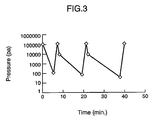
- Fig. 1 (e) two sets 10 of 180 sheets of board material 1 stacked are prepared and placed in vacuum chamber 11, and board material 1b is dried.
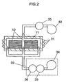
- Fig. 2 shows a schematic diagram of a dryer in accordance with the present invention.
- Pre-heater 31 are provided around vacuum chamber 11, and a vacuum system comprising a vacuum pump 32, and foreign substance removing filter 35 for protecting vacuum pump 32 is connected to the chamber.
- the dryer has hot air supplier 33 comprising hot air generator 34, foreign substance removing filter 35, and air dryer 36 for pressurizing the chamber.
- Board material 1b placed in vacuum chamber 11 is evacuated and dried while being heated by radiation heat radiated from pre-heater 31.
- microwaves can be used for drying.
- conductive paste 14 is filled in through holes 5 using such means as printing.
- through holes 5 have a proper shape, the inside of through holes 5 can completely be filled with conductive paste 14 without hindrance.
- mask films made of PET sheets 2a and 2b are stripped off.
- board material 1b is sandwiched by metal foils 15 and heated and pressed using a hot press (not shown). This operation completely cures board material 1b that has been in the pre-preg state and electrically connects metal foils 15 bonded to the both sides of board material 1b together via conductive paste 14.
- metallic foils 15 are patterned to a desired pattern and a double-sided circuit board that has circuit patterns 16 as shown in Fig. 1 (h) is obtained.
- the drying method in accordance with this embodiment can also be used for drying a double-sided circuit board that has been washed after the patterning.
- a method and a system of manufacturing a circuit board in accordance with the present invention comprise the following steps.
- the altered substances are formed on the surface of the board material and the inner wall of the through-holes or blind holes. Removing water drops that have attached to the surface of the board material in the cleaning step.
Landscapes
- Engineering & Computer Science (AREA)
- Manufacturing & Machinery (AREA)
- Microelectronics & Electronic Packaging (AREA)
- Mechanical Engineering (AREA)
- Life Sciences & Earth Sciences (AREA)
- Molecular Biology (AREA)
- Health & Medical Sciences (AREA)
- General Engineering & Computer Science (AREA)
- Manufacturing Of Printed Wiring (AREA)
- Drying Of Solid Materials (AREA)
- Non-Metallic Protective Coatings For Printed Circuits (AREA)
- Printing Elements For Providing Electric Connections Between Printed Circuits (AREA)
- Details Of Cutting Devices (AREA)
- Production Of Multi-Layered Print Wiring Board (AREA)
Abstract
Description
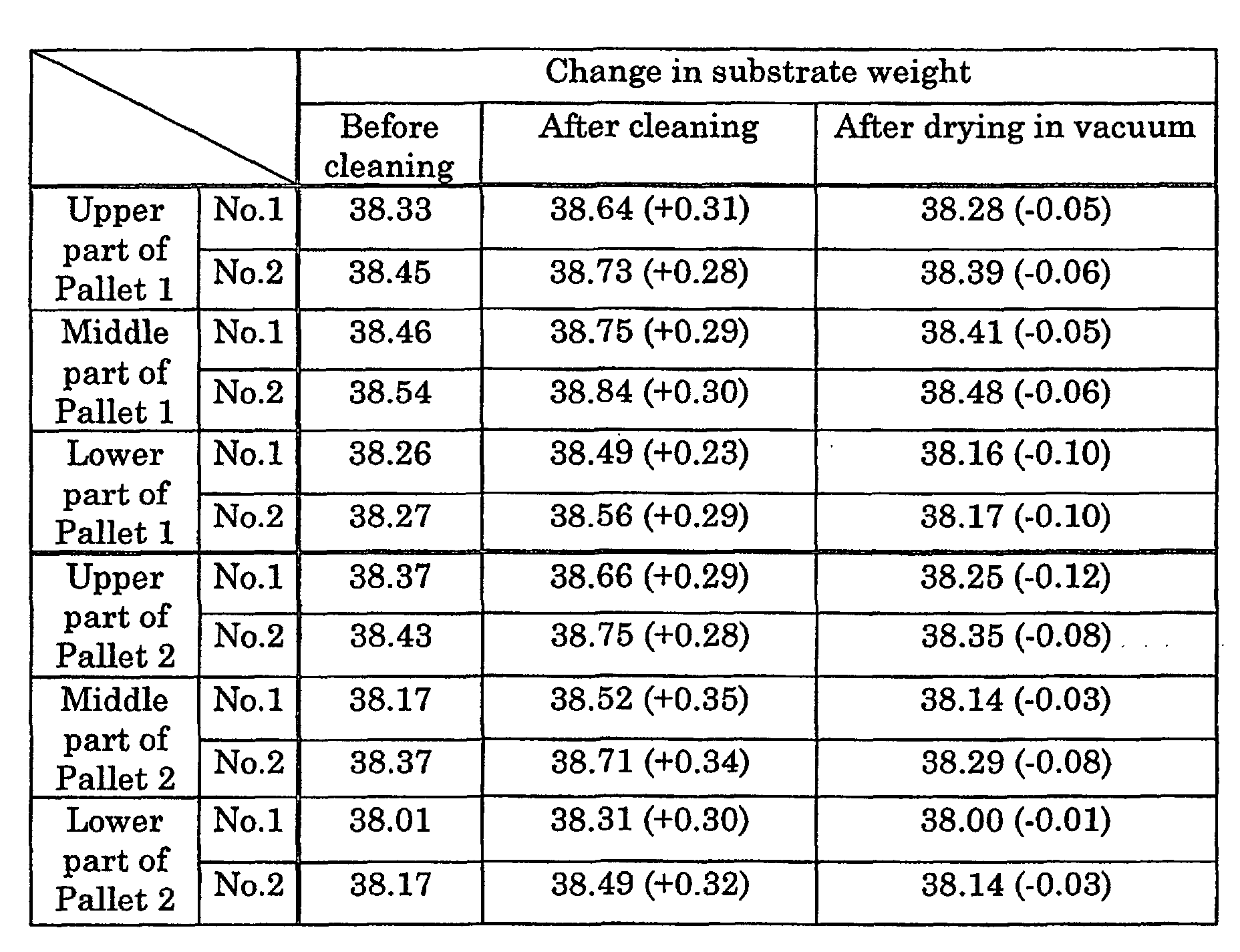
In the above processes: temperature of dry air: 60 °C
Total process time: approx. 40 minutes
Claims (36)
- A method of drying material comprising the steps of:wherein said evacuating and supplying steps are operated at least once.evacuating air in a vacuum chamber containing said material under an atmospheric pressure to an ultimate pressure; andsupplying air to said vacuum chamber to make a pressure in said chamber to an atmospheric pressure again,
- The method of drying material according to claim 1, wherein said ultimate pressure is gradually decreased as a number of said operation of evacuating and supplying steps increases.
- The method of drying material according to claim 1 further comprising the steps of:supplying hot air into said chamber when said chamber is made to the atmospheric pressure again; andevacuating again said chamber while said hot air is supplied to said vacuum chamber;stop supplying said hot air after a predetermined time duration; andevacuating to said ultimate pressure, in said supplying step.
- The method of drying material according to claim 3, wherein said predetermined time duration is at least one second.
- The method of drying material according to claim 1, wherein said steps are performed while material in said vacuum chamber is heated.
- The method of drying material according to claim 3, wherein air pressure of said hot air supplied is lower than air pressure in a previous evacuating step in one of a evacuating step performed thereafter.
- The method of drying material according to claim 3, wherein a temperature of said hot air is at least 35 °C.
- The method of drying material according to claim 1, wherein said supplying of air to said vacuum chamber is performed from a plurality of points.
- The method of drying material according to claim 1, wherein said evacuating of said vacuum chamber is performed from a plurality of points.
- The method of drying material according to claim 1, wherein said air to be supplied is dry air.
- The method of drying material according to claim 10, wherein said dry air is passed through at least one of an air cleaner and a dehumidifier.
- The method of drying material according to claim 1, wherein said ultimate pressure is at most 200 Pa.
- The method of drying material according to claim 5, wherein said material is heated using radiation heat from a heater.
- The method of drying material according to claim 5, wherein said material is heated using dielectric heating by microwaves.
- A dryer comprising a material container of a sealable structure, wherein said container has an air outlet and an air inlet, said air outlet and air inlet are piped to a evacuator and an air supplier, respectively, and said container has a heating means.
- The dryer according to claim 15, wherein said evacuator and said air supplier can operate repeatedly in one of a simultaneous manner and an alternate manner.
- The dryer according to claim 15, wherein said air supplier has a means for heating air and a means for removing at least one of foreign substance and moisture in air.
- The dryer according to claim 15, wherein said container has a plurality of air inlets.
- The dryer according to claim 15, wherein said container has a plurality of air outlets.
- The dryer according to claim 15, wherein a means for removing at least one of foreign substance and moisture in air is placed between said air outlet and said evacuator.
- The dryer according to claim 15, wherein said heating means uses radiation heat from a heater.
- The dryer according to claim 15, wherein said heating means uses dielectric heating by microwaves.
- The dryer according to claim 15 further comprising the following operation systems:(1) a system for actuating said heating means to heat a material in said container;(2) a system for actuating said evacuator, and stopping the evacuating operation after said container has reached to a predetermined vacuum pressure;(3) a system for actuating said air supplier to supply air to said container;(4) a system for actuating said evacuator to exhaust the air in said container;(5) a system for stopping said air supply operation after a predetermined period of time; and(6) a system for stopping the evacuating operation after reaching to a predetermined vacuum pressure.
- The dryer according to claim 15 comprising an operation system wherein said operations (1) to (6) are repeated a plurality of times.
- The material dryer according to claim 15, wherein said predetermined vacuum pressure in operation (6) of Claim 23 can be set lower than said predetermined vacuum pressure in operation (2) of Claim 23.
- The dryer according to claim 24, wherein said predetermined vacuum is set lower every time the number said repeating of said operation to be performed a plurality of times increases.
- A method of manufacturing a circuit board comprising the steps of:bonding a film shape material to at least one surface of a substrate material to form a board material with a film;forming one of a through hole and a blind hole by irradiating said board material with a film with laser;cleaning said board material to remove at least one of altered parts and altered substances formed on an inner wall of one of said through hole and said blind hole, and to remove foreign substance adhering to a surface of said board material with a film;blowing gas onto the surface of said board material with a film to remove water drops adhering to said surface;drying moisture adhering to and absorbed in said board material with a film, using the method of drying according to claim 1; andforming an electrical connection means in one of said through hole and said blind hole.
- A method of manufacturing a circuit board comprising the steps of:bonding a film-shape material to at least one surface of a substrate material to form a board material with a film;forming one of a through hole and a blind hole by irradiating said board material with a film with laser;filling one of said through hole and said blind hole with conductive paste;drying a double-sided circuit board having circuit patterns on both surfaces thereof, using the method of drying according to claim 1; andlaminating said double-sided circuit board and said board material to form a multi-layer circuit board, said board material being filled with conductive paste and said film-shape materials on the both sides of said board material being peeled off.
- A method of manufacturing a circuit board comprising the steps of:wherein moisture contained in said circuit board is removed using the method of drying according to claim 1.removing moisture of a circuit board having a circuit pattern on at least one surface thereof;bonding a board material to at least one surface of said circuit board;laminating said circuit board and said substrate material by further bonding a metal foil on said board material, and heating and pressing said circuit board and said substrate material at the same time; andforming a means for electrically connecting said circuit board and said metal foil,
- The method of manufacturing a circuit board according to claim 27, wherein said substrate material comprises a prepreg, said prepreg being made by impregnating a reinforcing material with a thermosetting resin and making the resin into B stage.
- The method of manufacturing a circuit board according to claim 30, wherein said reinforcing material is one of a glass fiber fabric and a glass fiber non-woven fabric.
- The method of manufacturing a circuit board according to claim 30, wherein said reinforcing material is one of an aromatic polyamide fiber fabric and an aromatic polyamide fiber non-woven fabric.
- The method of manufacturing a circuit board according to claim 27, wherein said forming an electrical connection means is a method of filling said hole with paste containing conductive particles.
- The method of manufacturing a circuit board according to claim 27, wherein forming an electrical connection means is a method of forming a plating layer on an inner wall of said hole.
- The method of manufacturing a circuit board according to claim 27, wherein one of said board material and said circuit board is dried under a state of stacking sheets of one of said board material and said circuit board one on top of another.
- The method of manufacturing a circuit board according to claim 27, wherein said film-shape material is coated with a thermosetting epoxy resin on a surface thereof.
Applications Claiming Priority (3)
| Application Number | Priority Date | Filing Date | Title |
|---|---|---|---|
| JP2000171539 | 2000-06-08 | ||
| JP2000171539 | 2000-06-08 | ||
| PCT/JP2001/004819 WO2001095682A1 (en) | 2000-06-08 | 2001-06-07 | Method and device for drying materials and method of producing circuit boards using the same |
Publications (2)
| Publication Number | Publication Date |
|---|---|
| EP1289356A1 true EP1289356A1 (en) | 2003-03-05 |
| EP1289356A4 EP1289356A4 (en) | 2008-05-21 |
Family
ID=18674075
Family Applications (1)
| Application Number | Title | Priority Date | Filing Date |
|---|---|---|---|
| EP01938558A Withdrawn EP1289356A4 (en) | 2000-06-08 | 2001-06-07 | METHOD AND DEVICE FOR DRYING MATERIALS AND PROCESS FOR PRODUCING INTEGRATED CIRCUIT CARDS USING THE SAME |
Country Status (6)
| Country | Link |
|---|---|
| US (1) | US6893530B2 (en) |
| EP (1) | EP1289356A4 (en) |
| JP (1) | JP3815435B2 (en) |
| CN (1) | CN1196388C (en) |
| TW (1) | TW595284B (en) |
| WO (1) | WO2001095682A1 (en) |
Cited By (2)
| Publication number | Priority date | Publication date | Assignee | Title |
|---|---|---|---|---|
| CN100456908C (en) * | 2003-11-28 | 2009-01-28 | 顶瑞机械股份有限公司 | Printed circuit board protective film hot pressing method |
| US8216623B2 (en) | 2009-04-07 | 2012-07-10 | Frito-Lay North America, Inc. | Flavor infused nut snack |
Families Citing this family (29)
| Publication number | Priority date | Publication date | Assignee | Title |
|---|---|---|---|---|
| US8701307B2 (en) | 2008-09-17 | 2014-04-22 | Howard C. Slack | Method for cleaning and reconditioning FCR APG-68 tactical radar units |
| US8673156B2 (en) * | 2008-10-02 | 2014-03-18 | Gryphon Environmental, Llc | Suspension liquid extraction apparatus and method |
| US8230616B2 (en) * | 2009-06-11 | 2012-07-31 | Sterilucent, Inc. | Apparatus and method for drying and sterilizing objects in a load |
| JP5742114B2 (en) | 2010-05-17 | 2015-07-01 | 日産自動車株式会社 | Drying method and drying apparatus |
| CN101915498B (en) * | 2010-08-06 | 2011-12-07 | 爱阔特(上海)清洗设备制造有限公司 | Intelligent vacuum drying method |
| CN102692115A (en) * | 2011-03-25 | 2012-09-26 | 漳州弘烨机械制造有限公司 | Novel low-temperature roasting technique and equipment thereof |
| CN102548197B (en) * | 2012-01-30 | 2016-08-03 | 华为技术有限公司 | A kind of High-Speed Printed Circuit Board |
| WO2016105505A1 (en) | 2014-12-23 | 2016-06-30 | Revive Electronics, LLC | Apparatuses and methods for controlling power to electronic devices |
| US12276454B2 (en) | 2020-04-21 | 2025-04-15 | Revive Electronics, LLC | Methods and apparatuses for drying electronic devices |
| US12215925B2 (en) | 2020-04-21 | 2025-02-04 | Revive Electronics, LLC | Methods and apparatuses for drying electronic devices |
| US9644891B2 (en) | 2012-02-01 | 2017-05-09 | Revive Electronics, LLC | Methods and apparatuses for drying electronic devices |
| US10876792B2 (en) | 2012-02-01 | 2020-12-29 | Revive Electronics, LLC | Methods and apparatuses for drying electronic devices |
| US11713924B2 (en) | 2012-02-01 | 2023-08-01 | Revive Electronics, LLC | Methods and apparatuses for drying electronic devices |
| US10690413B2 (en) | 2012-02-01 | 2020-06-23 | Revive Electronics, LLC | Methods and apparatuses for drying electronic devices |
| BR112014018989B1 (en) | 2012-02-01 | 2022-03-03 | Revive Electronics, LLC | Method and apparatus for drying an electronic device, device and method for removing wetting from an electronic device, and, method for manufacturing a device |
| US10240867B2 (en) | 2012-02-01 | 2019-03-26 | Revive Electronics, LLC | Methods and apparatuses for drying electronic devices |
| US12281847B2 (en) | 2020-04-21 | 2025-04-22 | Revive Electronics, LLC | Methods and apparatuses for drying electronic devices |
| US9970708B2 (en) | 2012-02-01 | 2018-05-15 | Revive Electronics, LLC | Methods and apparatuses for drying electronic devices |
| WO2014037509A1 (en) * | 2012-09-07 | 2014-03-13 | Novozymes A/S | Method of drying textile using alternating pressure |
| US20140093643A1 (en) * | 2012-09-28 | 2014-04-03 | Tyco Electronics Services Gmbh | Method and system of depositing a viscous material into a surface cavity |
| US8689461B1 (en) * | 2012-11-08 | 2014-04-08 | TekDry, LLC | Dryer for portable electronics |
| US10088230B2 (en) | 2012-11-08 | 2018-10-02 | Tekdry International, Inc. | Dryer for portable electronics |
| US9488565B2 (en) | 2012-11-14 | 2016-11-08 | Revive Electronics, LLC | Method and apparatus for detecting moisture in portable electronic devices |
| CN103108489B (en) * | 2013-01-10 | 2016-04-27 | 厦门大学 | Use in printed circuit board bonding sheet microwave irradiation devices and methods therefor |
| WO2014153007A1 (en) * | 2013-03-14 | 2014-09-25 | Revive Electronics, LLC | Methods and apparatuses for drying electronic devices |
| CN105555036A (en) * | 2016-02-02 | 2016-05-04 | 东莞翔国光电科技有限公司 | Manufacturing process for printed circuit board through physical method |
| US12510296B2 (en) | 2020-04-21 | 2025-12-30 | Revive Electronics, LLC | Methods and apparatuses for drying electronic devices |
| US12584689B2 (en) | 2020-04-21 | 2026-03-24 | Revive Electronics, LLC | Methods and apparatuses for drying electronic devices |
| CN118757996B (en) * | 2024-09-05 | 2025-01-21 | 中国电子科技集团公司第五十五研究所 | Method for controlling water vapor content inside highly integrated microwave components |
Family Cites Families (21)
| Publication number | Priority date | Publication date | Assignee | Title |
|---|---|---|---|---|
| US1902575A (en) * | 1930-01-23 | 1933-03-21 | Allis Chalmers Mfg Co | Method of treating objects |
| AU1264466A (en) * | 1967-10-17 | 1969-04-24 | Arthur Leonard Bigg-Wither | Improvements in drying apparatus |
| DE1930210A1 (en) * | 1969-06-13 | 1971-01-07 | Bayer Ag | Process and device for drying materials in vacuum drying systems to a predeterminable material moisture content |
| DE3371244D1 (en) * | 1983-10-08 | 1987-06-04 | Mtm Obermaier Gmbh & Co Kg | Process and apparatus for drying yarn or fibre packages |
| JPS6155372A (en) | 1984-08-25 | 1986-03-19 | Shimadzu Corp | Rotary fluid energy converter |
| JPS6155372U (en) * | 1984-09-18 | 1986-04-14 | ||
| DK59286D0 (en) * | 1986-02-06 | 1986-02-06 | Steen Ole Moldrup | PROCEDURE AND PLANT TO REMOVE WOOD FROM WOOD |
| US4977688A (en) * | 1989-10-27 | 1990-12-18 | Semifab Incorporated | Vapor device and method for drying articles such as semiconductor wafers with substances such as isopropyl alcohol |
| CA2040989A1 (en) * | 1990-05-01 | 1991-11-02 | Ichiro Yoshida | Washing/drying method and apparatus |
| JPH07109937B2 (en) | 1990-08-13 | 1995-11-22 | アイカ工業株式会社 | Laminated product manufacturing method |
| JPH04132388U (en) * | 1991-05-24 | 1992-12-08 | 千住金属工業株式会社 | vacuum dryer |
| JP2601128B2 (en) | 1992-05-06 | 1997-04-16 | 松下電器産業株式会社 | Method of manufacturing circuit forming substrate and circuit forming substrate |
| JPH067750A (en) * | 1992-06-29 | 1994-01-18 | Nippon Seiko Kk | Vacuum degreasing and drying method |
| US5273589A (en) * | 1992-07-10 | 1993-12-28 | Griswold Bradley L | Method for low pressure rinsing and drying in a process chamber |
| JPH07243765A (en) * | 1994-03-04 | 1995-09-19 | Hitachi Ltd | Heating dryer |
| US5732478A (en) * | 1996-05-10 | 1998-03-31 | Altos Engineering, Inc. | Forced air vacuum drying |
| JP3776977B2 (en) * | 1996-06-14 | 2006-05-24 | 大日本印刷株式会社 | Vacuum drying equipment |
| CN2286521Y (en) | 1996-07-23 | 1998-07-22 | 台州进出口商品检验局职工技术协会 | Ambient temp. vacuum drying machine |
| JPH1143384A (en) * | 1997-07-28 | 1999-02-16 | Matsushita Electric Works Ltd | Production of inorganic board |
| JP3149837B2 (en) * | 1997-12-08 | 2001-03-26 | 松下電器産業株式会社 | Method and apparatus for manufacturing circuit forming substrate and material for circuit forming substrate |
| JP3238901B2 (en) * | 1998-07-16 | 2001-12-17 | 松下電器産業株式会社 | Multilayer printed wiring board and method of manufacturing the same |
-
2001
- 2001-06-07 JP JP2002501851A patent/JP3815435B2/en not_active Expired - Fee Related
- 2001-06-07 WO PCT/JP2001/004819 patent/WO2001095682A1/en not_active Ceased
- 2001-06-07 EP EP01938558A patent/EP1289356A4/en not_active Withdrawn
- 2001-06-07 TW TW090113809A patent/TW595284B/en not_active IP Right Cessation
- 2001-06-07 CN CNB018015948A patent/CN1196388C/en not_active Expired - Fee Related
-
2002
- 2002-02-08 US US10/068,025 patent/US6893530B2/en not_active Expired - Fee Related
Cited By (2)
| Publication number | Priority date | Publication date | Assignee | Title |
|---|---|---|---|---|
| CN100456908C (en) * | 2003-11-28 | 2009-01-28 | 顶瑞机械股份有限公司 | Printed circuit board protective film hot pressing method |
| US8216623B2 (en) | 2009-04-07 | 2012-07-10 | Frito-Lay North America, Inc. | Flavor infused nut snack |
Also Published As
| Publication number | Publication date |
|---|---|
| TW595284B (en) | 2004-06-21 |
| WO2001095682A1 (en) | 2001-12-13 |
| US20020173109A1 (en) | 2002-11-21 |
| JP3815435B2 (en) | 2006-08-30 |
| EP1289356A4 (en) | 2008-05-21 |
| CN1196388C (en) | 2005-04-06 |
| US6893530B2 (en) | 2005-05-17 |
| CN1383708A (en) | 2002-12-04 |
Similar Documents
| Publication | Publication Date | Title |
|---|---|---|
| US6893530B2 (en) | Method and system of drying materials and method of manufacturing circuit boards using the same | |
| JPWO2001095682A1 (en) | Material drying method and device, and circuit board manufacturing method using the same | |
| US6428942B1 (en) | Multilayer circuit structure build up method | |
| CN111033690B (en) | Multilayer circuit board using interposer layer and conductive paste | |
| US6546624B2 (en) | Removable film, a substrate with film, a process for forming the removable film and a process for the manufacturing of the circuit board | |
| CN100576980C (en) | Method for forming wiring on insulating resin layer | |
| JP2008277820A (en) | Method for making multilayered circuitized substrate | |
| JPH0590756A (en) | Production of rigid/flexible board | |
| US6838372B2 (en) | Via interconnect forming process and electronic component product thereof | |
| JP2006140531A (en) | Substrate material drying method | |
| JP2001251054A (en) | Method of manufacturing circuit board for multilayer printed wiring board | |
| EP1109429B1 (en) | A method of manufacturing a circuit board and its manufacturing apparatus | |
| WO1998049877A1 (en) | Apparatus for manufacturing adhesive layer, apparatus for manufacturing double-sided substrate, and apparatus for manufacturing multi-layered substrate | |
| JPH08279678A (en) | Manufacture of multilayered printed wiring board | |
| JP4455696B2 (en) | Multilayer printed wiring board manufacturing method and manufacturing apparatus | |
| US6203652B1 (en) | Method of forming a via in a substrate | |
| JP3149808B2 (en) | Manufacturing method of circuit forming substrate | |
| JP2000216521A (en) | Wiring board manufacturing method and wiring board using the same | |
| JPH10224041A (en) | Multilayer wiring board and method of manufacturing the same | |
| JP2001237521A (en) | Method and apparatus for manufacturing circuit forming substrate | |
| JP2002252463A (en) | Build-up wiring board and its manufacturing method | |
| KR100865120B1 (en) | Manufacturing method of multilayer printed circuit board using inkjet printing method | |
| JP2007281431A (en) | Method of manufacturing circuit board | |
| JP2000315863A (en) | Manufacturing method of multilayer printed wiring board | |
| JPH09117714A (en) | Dust removing method |
Legal Events
| Date | Code | Title | Description |
|---|---|---|---|
| PUAI | Public reference made under article 153(3) epc to a published international application that has entered the european phase |
Free format text: ORIGINAL CODE: 0009012 |
|
| 17P | Request for examination filed |
Effective date: 20020226 |
|
| AK | Designated contracting states |
Designated state(s): AT BE CH CY DE DK ES FI FR GB GR IE IT LI LU MC NL PT SE TR Kind code of ref document: A1 Designated state(s): AT BE CH CY DE DK ES FI FR GB GR IE IT LI LU MC NL PT SE TR |
|
| RBV | Designated contracting states (corrected) |
Designated state(s): DE FR GB |
|
| A4 | Supplementary search report drawn up and despatched |
Effective date: 20080418 |
|
| 17Q | First examination report despatched |
Effective date: 20080813 |
|
| RAP1 | Party data changed (applicant data changed or rights of an application transferred) |
Owner name: PANASONIC CORPORATION |
|
| STAA | Information on the status of an ep patent application or granted ep patent |
Free format text: STATUS: THE APPLICATION IS DEEMED TO BE WITHDRAWN |
|
| 18D | Application deemed to be withdrawn |
Effective date: 20140520 |