EP1289353A1 - Surface mounting type electronic component - Google Patents

Surface mounting type electronic component Download PDF

Info

Publication number
EP1289353A1
EP1289353A1 EP02714512A EP02714512A EP1289353A1 EP 1289353 A1 EP1289353 A1 EP 1289353A1 EP 02714512 A EP02714512 A EP 02714512A EP 02714512 A EP02714512 A EP 02714512A EP 1289353 A1 EP1289353 A1 EP 1289353A1
Authority
EP
European Patent Office
Prior art keywords
electronic component
case
board
leg
surface mounted
Prior art date
Legal status (The legal status is an assumption and is not a legal conclusion. Google has not performed a legal analysis and makes no representation as to the accuracy of the status listed.)
Withdrawn
Application number
EP02714512A
Other languages
German (de)
French (fr)
Other versions
EP1289353A4 (en
Inventor
Masato Yamasaki
Koji Ono
Takumi Nishimoto
Jun Sato
Current Assignee (The listed assignees may be inaccurate. Google has not performed a legal analysis and makes no representation or warranty as to the accuracy of the list.)
Panasonic Holdings Corp
Original Assignee
Matsushita Electric Industrial Co Ltd
Priority date (The priority date is an assumption and is not a legal conclusion. Google has not performed a legal analysis and makes no representation as to the accuracy of the date listed.)
Filing date
Publication date
Application filed by Matsushita Electric Industrial Co Ltd filed Critical Matsushita Electric Industrial Co Ltd
Publication of EP1289353A1 publication Critical patent/EP1289353A1/en
Publication of EP1289353A4 publication Critical patent/EP1289353A4/en
Withdrawn legal-status Critical Current

Links

Images

Classifications

    • HELECTRICITY
    • H01ELECTRIC ELEMENTS
    • H01GCAPACITORS; CAPACITORS, RECTIFIERS, DETECTORS, SWITCHING DEVICES, LIGHT-SENSITIVE OR TEMPERATURE-SENSITIVE DEVICES OF THE ELECTROLYTIC TYPE
    • H01G2/00Details of capacitors not covered by a single one of groups H01G4/00-H01G11/00
    • H01G2/02Mountings
    • H01G2/06Mountings specially adapted for mounting on a printed-circuit support
    • H01G2/065Mountings specially adapted for mounting on a printed-circuit support for surface mounting, e.g. chip capacitors
    • HELECTRICITY
    • H01ELECTRIC ELEMENTS
    • H01CRESISTORS
    • H01C1/00Details
    • H01C1/14Terminals or tapping points specially adapted for resistors; Arrangements of terminals or tapping points on resistors
    • H01C1/144Terminals or tapping points specially adapted for resistors; Arrangements of terminals or tapping points on resistors the terminals or tapping points being welded or soldered
    • HELECTRICITY
    • H05ELECTRIC TECHNIQUES NOT OTHERWISE PROVIDED FOR
    • H05KPRINTED CIRCUITS; CASINGS OR CONSTRUCTIONAL DETAILS OF ELECTRIC APPARATUS; MANUFACTURE OF ASSEMBLAGES OF ELECTRICAL COMPONENTS
    • H05K3/00Apparatus or processes for manufacturing printed circuits
    • H05K3/30Assembling printed circuits with electric components, e.g. with resistors
    • H05K3/32Assembling printed circuits with electric components, e.g. with resistors electrically connecting electric components or wires to printed circuits
    • H05K3/34Assembling printed circuits with electric components, e.g. with resistors electrically connecting electric components or wires to printed circuits by soldering
    • H05K3/341Surface mounted components
    • H05K3/3421Leaded components
    • H05K3/3426Leaded components characterised by the leads
    • HELECTRICITY
    • H01ELECTRIC ELEMENTS
    • H01HELECTRIC SWITCHES; RELAYS; SELECTORS; EMERGENCY PROTECTIVE DEVICES
    • H01H1/00Contacts
    • H01H1/58Electric connections to or between contacts; Terminals
    • H01H2001/5888Terminals of surface mounted devices [SMD]
    • YGENERAL TAGGING OF NEW TECHNOLOGICAL DEVELOPMENTS; GENERAL TAGGING OF CROSS-SECTIONAL TECHNOLOGIES SPANNING OVER SEVERAL SECTIONS OF THE IPC; TECHNICAL SUBJECTS COVERED BY FORMER USPC CROSS-REFERENCE ART COLLECTIONS [XRACs] AND DIGESTS
    • Y02TECHNOLOGIES OR APPLICATIONS FOR MITIGATION OR ADAPTATION AGAINST CLIMATE CHANGE
    • Y02PCLIMATE CHANGE MITIGATION TECHNOLOGIES IN THE PRODUCTION OR PROCESSING OF GOODS
    • Y02P70/00Climate change mitigation technologies in the production process for final industrial or consumer products
    • Y02P70/50Manufacturing or production processes characterised by the final manufactured product

Definitions

  • the present invention relates to a surface mounted electronic component mounted on a surface of a printed circuit board in various electronic instruments and having a function, such as an encoder, a variable resistor, or a switch.
  • a surface mounted electronic component (it is called electronic component hereinafter) has been preferably used.
  • the electronic component is mainly a chip type electronic component, but is an electronic component having a function, such as an encoder, a variable resistor, or a switch, which is utilized with an operation knob mounted to an operating shaft.
  • the electronic component has an output terminal out of a case and a board mounting part, such as a leg, mounted to the case.
  • the board mounting part is soldered to a land of a component-soldered part on the printed circuit board, thereby assuring mounting strength of the electronic component.
  • a material used for the board mounting part of the electronic component is thinned or narrowed, thereby downsizing and thinning the electronic component and reducing its material.
  • Fig, 8 is a front view of the conventional surface mounted electronic component.
  • Fig. 9 is a side view of the component.
  • Fig. 10 is a top view of the component.
  • the surface mounted electronic component 1 includes a resin case 2 and a leg 3 as the board mounting part.
  • the leg 3 made of metallic flat plate projects outward from a side of the case 2, is bent toward the bottom side of the case 2 at a predetermined position, and extends along a side wall of the case 2.
  • the leg 3 has a soldering part 3A projecting outward from a bottom surface position of the case 2.
  • the soldering part 3A is bent near the case 2 laterally by approximately 90°.
  • the leg 3 is disposed on each sides of the case 2 opposite to each other of the electronic component 1.
  • the case 2 accommodates a functioning component, such as an encoder, a variable resistor, or a switch, and the output terminal is guided out of the case 2 (not shown).
  • a functioning component such as an encoder, a variable resistor, or a switch
  • a printed circuit board 11 for accepting the electronic component 1 has two lands 12 soldered to the soldering parts 3A of the legs 3, as shown in a perspective view of Fig. 11.
  • the electronic component 1 is mounted through having the output terminals (not shown) soldered to a predetermined pattern (not shown) on the printed circuit board 11 and through having the soldering parts 3A as the board mounting parts soldered to the lands 12 on the board 11. While being mounted, even if an external force P is applied to the side of the electronic component 1, the electronic component 1 absorbs the external force P with connection between the board mounting parts (the legs 3) and the board 11.
  • the leg 3 must be narrowed, shortened, and thinned. This structure accordingly reduces the soldering strength of the soldering part 3A to the board 11 and the strength of the leg 3 itself, so that shortage of the strength against the external force P is concerned.
  • a surface mounted electronic component includes a case, a leg extending from the case, and a board mounting part at a tip of the leg.
  • the leg includes a projection extending in an extending direction of the leg from the case, and an outer frame formed perpendicularly to the projection away from the case.
  • the surface mounted electronic component keeps to be mounted tightly to a circuit board even when an external force is applied to the electronic component.
  • Fig. 1 is a front view of a surface mounted electronic component in accordance with an exemplary embodiment of the present invention.
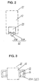
  • Fig. 2 is a side view of the component, and
  • Fig. 3 is a top view of the component.
  • a surface mounted electronic component 21 includes a resin case 22 substantially square in its top view and fixtures made of metal plate fixed to the case 22. A tip of the leg 23 of each fixture extends downward along a side surface of the case 22 functions as a board mounting part 51.
  • the leg 23 may extend integrally on the side surface of a fixture mounted as to cover the case 22.
  • the tip of the leg 23 includes an outer frame 23A having the same width as that of the leg 23.
  • the outer frame 23A is bent outward by approximately 90° from the leg 23 at a height equal to a bottom surface of the case 22.
  • the outer frame 23A is perpendicular to the leg 23, as shown in Fig. 3.
  • the outer frame 23A has a substantially square U-shaped tip having its opening towards the case 22.
  • the tip of the outer frame 23A is integrally connected to the leg 23, and the integrated structure has a penetration hole 25 at a center from top view.
  • a central position of a portion of the leg 23 connected with the opening of the outer frame 23A is provided with a projection 23B.
  • the projection 23B projects under the bottom of the case 22, and is formed unitarily with the leg 23 in its extending direction.
  • the board mounting part 51 of the present embodiment includes the outer frame 23A and the projection 23B that are orthogonal to each other.
  • the board mounting parts 51 are disposed on facing edges of the four edges constituting the outer periphery of the case 22, respectively.
  • the facing edges are different from the edges having an output terminal (not shown).
  • a tip of the leg 23 formed at a predetermined width is punched to form an upward square U-shaped opening.
  • the opening corresponds to the through hole 25.
  • the remaining part of the tip of the leg 23 is machined in a frame shape with the predetermined width. Then, the remaining part is bent perpendicularly at broken lines of Fig. 4 so as to separate the tip from the case 22 to form the outer frame 23A.
  • the outer frame 23A has a frame shape, and thus, a deviation of the lateral bending position is small, thus allowing the frame to be bent easily and accurately. Therefore, the projection 23B from the leg 23 is consequently positioned accurately.
  • the board mounting part 51 is simply and accurately formed of a part coaxial with the leg 23 without material loss.
  • a printed circuit board 31 for accepting the electronic component 21 including the board mounting parts 51 has a substantially quadrangular lands 32A at positions corresponding to the outer frames 23A of the legs 23, as shown in Fig. 5.
  • the lands 32A are used as mounted parts 32 for the board mounting parts 51, and are larger than the outer frames 23A.
  • a central part at an edge of each land 32A includes a hole 32B, where the projection 23B passes, disposed on the leg 23.
  • the electronic component 21 includes the board mounting parts 51 facing each other, the mounted parts 32 corresponding to them faces each other on the printed board 31 with the edges having the holes 32B as inner edges.
  • the board 31 includes a land corresponding to an output terminal and a pattern connected to the land (not shown).
  • cream solder is applied to the land corresponding to the output terminal on the board 31, and cream solder is also applied to the lands 32A of the mounted parts 32, as shown in Fig. 6.
  • the projections 23B are inserted into the holes 32B to mount the electronic component 21 on the board 31.
  • the cream solder upon being melted, connects the outer frames 23A to the land parts 32A of the mounted parts 32 and simultaneously, connects the output terminal to the land.
  • the electronic component 21 is easily supported by itself even when the electronic component 21 is placed on the printed board 31. Additionally, a displacement of the electronic component 21 due to a movement in a manufacturing process until the soldering, and the vibration can be reduced.
  • the clearance if being such a size that the projection 23B is inserted into the hole 32B slightly press-fittingly, prevents the displacement and allows the electronic component 21 to be soldered accurately.
  • each outer frame 23A Since the entire lower surface of each outer frame 23A contacts with the cream solder, as discussed above, the inner end surface of the outer frame 23A including the penetration hole 25 as well as its outer end surface is certainly soldered, and is connected to the landts 32A on the board 31 at high connecting strength.
  • the electronic component 21 has the outer frames 23A thus tightly soldered to the lands 32A is soldered to the printed board 31. Therefore, even when an external force Q to tilt the electronic component 21 is applied to the electronic component 21 from a side direction or the like (Fig. 6), the projections 23B inserted into the holes 32B abut on side walls of the holes 32B to generate large resistance.
  • the accurately formed outer frames 23A are certainly soldered to the lands 32A having the edges parallel with the side surface of the case 22, and the penetration holes 25 in the outer frames 23A are filled with the solder in soldering. This reinforces the legs 23 of the electronic component 21. Even when the external force Q is applied, the electronic component 21 can be kept to be mounted normally for a long time. Even if fixtures forming the board mounting parts 51 is thin, for example, the electronic component 21 is tightly mounted.
  • the board mounting parts 51 are arranged so as to solder four edges on the outer periphery of the case 22, the board mounting parts 51 is tightly mounted regardless of the direction of the external force Q.
  • the projections 23B of the board mounting parts 51 are inserted into the holes 32B in the board 31 in the above example.
  • a printed circuit board 41 including mounted parts 43 having side walls processed into solderable as a through hole 43B may be used.
  • the output terminal of the electronic component 21 are soldered to the land, and the outer frames 23A are soldered to lands 43A of the mounted parts 43.
  • the projections 23B are also soldered to the through holes 43B, where the projections pass. This allows the electronic component 21 to be more tightly soldered and mounted to the printed board 41.
  • the side surfaces of the projections 23B are soldered and fixed to the side wall of the through holes 43B. This arrangement increases resistance to an undesired external force R transversely applied to the electronic component 21. Therefore, the electronic component 21 is kept to be mounted stably for a long time.
  • cream solder may be pressed into the holes 32B using the projections 23B when the projections 23B is inserted into the holes 32B, thus allowing the component to be mounted similarly.
  • patterns (not shown) connected to the mounted parts 32 and 43 for the board mounting parts 51 of the printed boards 31 and 41 accepting the electronic component 21 may be connected to a ground in a working instrument. Static electricity from an operation part of the instrument into the electronic component 21 flows to the ground via the legs 23 (the board mounting parts 51) and the patterns connected to the board mounting parts 51 of the boards 31 and 41. This prevents noise caused by the static electricity, thereby allowing a predetermined functional element accommodated in the case 22 of the electronic component 21 to output normally, for example, an encoder, a variable resistor, or a switch.
  • the board mounting parts 51 may be formed of a member other than fixtures, and provides similar advantageousness.
  • a surface mounted electronic component including a simplified board mounting part including an outer frame and a projection.
  • the outer frame and the projection can be formed accurately without material loss.

Landscapes

  • Engineering & Computer Science (AREA)
  • Microelectronics & Electronic Packaging (AREA)
  • Power Engineering (AREA)
  • Manufacturing & Machinery (AREA)
  • Structures For Mounting Electric Components On Printed Circuit Boards (AREA)
  • Mounting Components In General For Electric Apparatus (AREA)
  • Shielding Devices Or Components To Electric Or Magnetic Fields (AREA)
  • Switch Cases, Indication, And Locking (AREA)
  • Adjustable Resistors (AREA)
  • Electric Connection Of Electric Components To Printed Circuits (AREA)
  • Mounting Of Printed Circuit Boards And The Like (AREA)

Abstract

A surface mounted electronic component includes a case and a board mounting part. The board mounting part includes a leg bent in parallel with a printed circuit board at its tip, an outer frame soldered to a land of a mounted part on the board, and a projection disposed in the outer frame and inserted into a hole in the mounted part. The electronic component is mounted on a surface of the printed circuit board in various electronic instruments, and can keep to be mounted on the board tightly even when an external force is applied.

Description

FIELD OF THE INVENTION
The present invention relates to a surface mounted electronic component mounted on a surface of a printed circuit board in various electronic instruments and having a function, such as an encoder, a variable resistor, or a switch.
BACKGROUND OF THE INVENTION
Electronic instruments have recently been downsized and thinned, and this requires downsizing and thinning of electronic components used for them strongly. A surface mounted electronic component (it is called electronic component hereinafter) has been preferably used.
The electronic component is mainly a chip type electronic component, but is an electronic component having a function, such as an encoder, a variable resistor, or a switch, which is utilized with an operation knob mounted to an operating shaft.
The electronic component has an output terminal out of a case and a board mounting part, such as a leg, mounted to the case. The board mounting part is soldered to a land of a component-soldered part on the printed circuit board, thereby assuring mounting strength of the electronic component.
A material used for the board mounting part of the electronic component is thinned or narrowed, thereby downsizing and thinning the electronic component and reducing its material.
Such a conventional surface mounted electronic component having a board mounting part will be described hereinafter with reference to the accompanying drawings. Fig, 8 is a front view of the conventional surface mounted electronic component. Fig. 9 is a side view of the component. Fig. 10 is a top view of the component. The surface mounted electronic component 1 includes a resin case 2 and a leg 3 as the board mounting part.
The leg 3 made of metallic flat plate projects outward from a side of the case 2, is bent toward the bottom side of the case 2 at a predetermined position, and extends along a side wall of the case 2. The leg 3 has a soldering part 3A projecting outward from a bottom surface position of the case 2. The soldering part 3A is bent near the case 2 laterally by approximately 90°. The leg 3 is disposed on each sides of the case 2 opposite to each other of the electronic component 1.
The case 2 accommodates a functioning component, such as an encoder, a variable resistor, or a switch, and the output terminal is guided out of the case 2 (not shown).
A printed circuit board 11 for accepting the electronic component 1 has two lands 12 soldered to the soldering parts 3A of the legs 3, as shown in a perspective view of Fig. 11.
The electronic component 1 is mounted through having the output terminals (not shown) soldered to a predetermined pattern (not shown) on the printed circuit board 11 and through having the soldering parts 3A as the board mounting parts soldered to the lands 12 on the board 11. While being mounted, even if an external force P is applied to the side of the electronic component 1, the electronic component 1 absorbs the external force P with connection between the board mounting parts (the legs 3) and the board 11.
If the conventional surface mounted electronic component 1 having the legs 3 as the board mounting part is downsized and thinned, the leg 3 must be narrowed, shortened, and thinned. This structure accordingly reduces the soldering strength of the soldering part 3A to the board 11 and the strength of the leg 3 itself, so that shortage of the strength against the external force P is concerned.
SUMMARY OF THE INVENTION
A surface mounted electronic component includes a case, a leg extending from the case, and a board mounting part at a tip of the leg. The leg includes a projection extending in an extending direction of the leg from the case, and an outer frame formed perpendicularly to the projection away from the case.
The surface mounted electronic component keeps to be mounted tightly to a circuit board even when an external force is applied to the electronic component.
BRIEF DESCRIPTION OF THE DRAWINGS
  • Fig. 1 is a front view of a surface mounted electronic component in accordance with an exemplary embodiment of the present invention.
  • Fig. 2 is a side view of the surface mounted electronic component in accordance with the embodiment.
  • Fig. 3 is a top view of the surface mounted electronic component in accordance with the embodiment.
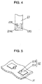
  • Fig. 4 is a side view for illustrating a method of forming a board mounting part of the surface mounted electronic component in accordance with the embodiment.
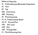
  • Fig. 5 is a perspective view of a printed circuit board for accepting the surface mounted electronic component in accordance with the embodiment.
  • Fig. 6 shows the board including the surface mounted electronic component mounted thereon in accordance with the embodiment.
  • Fig. 7 shows another printed circuit board including the surface mounted electronic component mounted thereon in accordance with the embodiment.
  • Fig. 8 is a front view of a conventional surface mounted electronic component.
  • Fig. 9 is a side view of the conventional surface mounted electronic component.
  • Fig. 10 is a top view of the conventional surface mounted electronic component.
  • Fig. 11 is a perspective view of a printed board for receiving the conventional surface mounted electronic component.
  • Fig. 12 shows the printed circuit board including the conventional surface mounted electronic component mounted thereon.
  • DETAILED DESCRIPTION OF THE PREFERRED EMBODIMENT
    Fig. 1 is a front view of a surface mounted electronic component in accordance with an exemplary embodiment of the present invention. Fig. 2 is a side view of the component, and Fig. 3 is a top view of the component. A surface mounted electronic component 21 includes a resin case 22 substantially square in its top view and fixtures made of metal plate fixed to the case 22. A tip of the leg 23 of each fixture extends downward along a side surface of the case 22 functions as a board mounting part 51.
    The leg 23 may extend integrally on the side surface of a fixture mounted as to cover the case 22.
    Detailed configurations of a fixing part between the case 22 and the fixture, an operating shaft projecting upward from the case 22, and the like are complicated, and thus, these are considered integrally as the case 22 in the drawings for simple explanation.
    The tip of the leg 23 includes an outer frame 23A having the same width as that of the leg 23. The outer frame 23A is bent outward by approximately 90° from the leg 23 at a height equal to a bottom surface of the case 22. The outer frame 23A is perpendicular to the leg 23, as shown in Fig. 3. The outer frame 23A has a substantially square U-shaped tip having its opening towards the case 22. The tip of the outer frame 23A is integrally connected to the leg 23, and the integrated structure has a penetration hole 25 at a center from top view.
    A central position of a portion of the leg 23 connected with the opening of the outer frame 23A is provided with a projection 23B. As shown in Fig. 2, the projection 23B projects under the bottom of the case 22, and is formed unitarily with the leg 23 in its extending direction.
    The board mounting part 51 of the present embodiment includes the outer frame 23A and the projection 23B that are orthogonal to each other.
    The board mounting parts 51 are disposed on facing edges of the four edges constituting the outer periphery of the case 22, respectively. The facing edges are different from the edges having an output terminal (not shown).
    For forming the board mounting part 51, a tip of the leg 23 formed at a predetermined width, as shown in the side view in Fig, 4, is punched to form an upward square U-shaped opening. The opening corresponds to the through hole 25. The remaining part of the tip of the leg 23 is machined in a frame shape with the predetermined width. Then, the remaining part is bent perpendicularly at broken lines of Fig. 4 so as to separate the tip from the case 22 to form the outer frame 23A. The outer frame 23A has a frame shape, and thus, a deviation of the lateral bending position is small, thus allowing the frame to be bent easily and accurately. Therefore, the projection 23B from the leg 23 is consequently positioned accurately.
    Thus, the board mounting part 51 is simply and accurately formed of a part coaxial with the leg 23 without material loss.
    A printed circuit board 31 for accepting the electronic component 21 including the board mounting parts 51 has a substantially quadrangular lands 32A at positions corresponding to the outer frames 23A of the legs 23, as shown in Fig. 5. The lands 32A are used as mounted parts 32 for the board mounting parts 51, and are larger than the outer frames 23A. A central part at an edge of each land 32A includes a hole 32B, where the projection 23B passes, disposed on the leg 23.
    Since the electronic component 21 includes the board mounting parts 51 facing each other, the mounted parts 32 corresponding to them faces each other on the printed board 31 with the edges having the holes 32B as inner edges.
    The board 31 includes a land corresponding to an output terminal and a pattern connected to the land (not shown).
    For mounting the electronic component 21 on the board 31, cream solder is applied to the land corresponding to the output terminal on the board 31, and cream solder is also applied to the lands 32A of the mounted parts 32, as shown in Fig. 6. The projections 23B are inserted into the holes 32B to mount the electronic component 21 on the board 31.
    At this moment, entire lower surfaces of the outer frames 23A are securely butted on the lands 32A. That is because the outer frames 23A orthogonal to the projections 23B are parallel with an upper surface of the board 31, and the outer frames 23A themselves are bent accurately with little deviation of the lateral bending position,
    Then, the cream solder, upon being melted, connects the outer frames 23A to the land parts 32A of the mounted parts 32 and simultaneously, connects the output terminal to the land.
    If a clearance between the projection 23B of each board mounting parts 51 and the hole 32B in the board 31 is small, the electronic component 21 is easily supported by itself even when the electronic component 21 is placed on the printed board 31. Additionally, a displacement of the electronic component 21 due to a movement in a manufacturing process until the soldering, and the vibration can be reduced. The clearance, if being such a size that the projection 23B is inserted into the hole 32B slightly press-fittingly, prevents the displacement and allows the electronic component 21 to be soldered accurately.
    Since the entire lower surface of each outer frame 23A contacts with the cream solder, as discussed above, the inner end surface of the outer frame 23A including the penetration hole 25 as well as its outer end surface is certainly soldered, and is connected to the landts 32A on the board 31 at high connecting strength.
    The electronic component 21 has the outer frames 23A thus tightly soldered to the lands 32A is soldered to the printed board 31. Therefore, even when an external force Q to tilt the electronic component 21 is applied to the electronic component 21 from a side direction or the like (Fig. 6), the projections 23B inserted into the holes 32B abut on side walls of the holes 32B to generate large resistance.
    Additionally, the accurately formed outer frames 23A are certainly soldered to the lands 32A having the edges parallel with the side surface of the case 22, and the penetration holes 25 in the outer frames 23A are filled with the solder in soldering. This reinforces the legs 23 of the electronic component 21. Even when the external force Q is applied, the electronic component 21 can be kept to be mounted normally for a long time. Even if fixtures forming the board mounting parts 51 is thin, for example, the electronic component 21 is tightly mounted.
    If the output terminal and the board mounting parts 51 are arranged so as to solder four edges on the outer periphery of the case 22, the board mounting parts 51 is tightly mounted regardless of the direction of the external force Q.
    The projections 23B of the board mounting parts 51 are inserted into the holes 32B in the board 31 in the above example. As shown in Fig. 7, a printed circuit board 41 including mounted parts 43 having side walls processed into solderable as a through hole 43B may be used. In this case, the output terminal of the electronic component 21 are soldered to the land, and the outer frames 23A are soldered to lands 43A of the mounted parts 43. The projections 23B are also soldered to the through holes 43B, where the projections pass. This allows the electronic component 21 to be more tightly soldered and mounted to the printed board 41. In other words, the side surfaces of the projections 23B are soldered and fixed to the side wall of the through holes 43B. This arrangement increases resistance to an undesired external force R transversely applied to the electronic component 21. Therefore, the electronic component 21 is kept to be mounted stably for a long time.
    Even when solder is not previously applied to the side walls of the through holes 43B in the former case, cream solder may be pressed into the holes 32B using the projections 23B when the projections 23B is inserted into the holes 32B, thus allowing the component to be mounted similarly.
    In either case, patterns (not shown) connected to the mounted parts 32 and 43 for the board mounting parts 51 of the printed boards 31 and 41 accepting the electronic component 21 may be connected to a ground in a working instrument. Static electricity from an operation part of the instrument into the electronic component 21 flows to the ground via the legs 23 (the board mounting parts 51) and the patterns connected to the board mounting parts 51 of the boards 31 and 41. This prevents noise caused by the static electricity, thereby allowing a predetermined functional element accommodated in the case 22 of the electronic component 21 to output normally, for example, an encoder, a variable resistor, or a switch.
    The board mounting parts 51 may be formed of a member other than fixtures, and provides similar advantageousness.
    INDUSTRIAL APPLICABILITY
    According to the present invention, a surface mounted electronic component including a simplified board mounting part including an outer frame and a projection. The outer frame and the projection can be formed accurately without material loss.

    Claims (6)

    1. A surface mounted electronic component comprising:
      a case;
      a leg extending from said case; and
      a board mounting part at a tip of said leg including:
      a projection extending in an extending direction of said leg from said case; and
      an outer frame formed perpendicularly to said projection away from said case.
    2. The surface mounted electronic component according to claim 1, wherein said projection is surrounded with said outer frame and said case.
    3. The surface mounted electronic component according to claim 1, further comprising:
      an output terminal disposed at a first edge of said case, said case being substantially square as seen from said extending direction of said leg,
         wherein said board mounting part is disposed at a second edge of said case.
    4. The surface mounted electronic component according to claim 1,
         wherein said projection is inserted into a hole formed in a circuit board, and
         wherein said outer frame is substantially parallel with said circuit board and is coupled to said circuit board.
    5. The surface mounted electronic component according to claim 4,
         wherein said circuit board includes a solderable part formed on a side wall of said hole, and
         wherein said inserted projection is soldered to said solderable part of said hole.
    6. The surface mounted electronic component according to claim 4, wherein said circuit board includes a mounted part coupled to a ground, said mounting part of said board being soldered to said outer frame.
    EP02714512A 2001-04-09 2002-04-05 SURFACE MOUNT TYPE ELECTRONIC COMPONENT Withdrawn EP1289353A4 (en)

    Applications Claiming Priority (3)

    Application Number Priority Date Filing Date Title
    JP2001109611 2001-04-09
    JP2001109611A JP2002305363A (en) 2001-04-09 2001-04-09 Surface mount electronic components
    PCT/JP2002/003464 WO2002085082A1 (en) 2001-04-09 2002-04-05 Surface mounting type electronic component

    Publications (2)

    Publication Number Publication Date
    EP1289353A1 true EP1289353A1 (en) 2003-03-05
    EP1289353A4 EP1289353A4 (en) 2004-09-01

    Family

    ID=18961524

    Family Applications (1)

    Application Number Title Priority Date Filing Date
    EP02714512A Withdrawn EP1289353A4 (en) 2001-04-09 2002-04-05 SURFACE MOUNT TYPE ELECTRONIC COMPONENT

    Country Status (5)

    Country Link
    US (1) US6828667B2 (en)
    EP (1) EP1289353A4 (en)
    JP (1) JP2002305363A (en)
    CN (1) CN1230049C (en)
    WO (1) WO2002085082A1 (en)

    Cited By (1)

    * Cited by examiner, † Cited by third party
    Publication number Priority date Publication date Assignee Title
    EP2791951A4 (en) * 2011-12-13 2015-11-11 Kemet Electronics Corp High aspect ratio stacked mlcc design

    Families Citing this family (13)

    * Cited by examiner, † Cited by third party
    Publication number Priority date Publication date Assignee Title
    JP4519724B2 (en) * 2005-07-01 2010-08-04 矢崎総業株式会社 Connector fixing structure
    JP4864419B2 (en) * 2005-10-28 2012-02-01 株式会社東芝 Printed circuit boards and electronic equipment
    JP2008258016A (en) * 2007-04-05 2008-10-23 Smk Corp Solder connection structure between electronic component terminals and printed wiring board
    JP4895035B2 (en) * 2007-05-14 2012-03-14 三洋電機株式会社 Solid electrolytic capacitor
    TWI403231B (en) * 2008-03-11 2013-07-21 Delta Electronics Inc Surface-mounted circuit board module and fabrication method thereof
    DE102009058825B4 (en) * 2009-12-18 2021-08-05 Webasto Ag Contact device for fastening to a circuit board, method for fastening a contact device to a circuit board and circuit board
    JP5619663B2 (en) * 2011-03-31 2014-11-05 古河電気工業株式会社 Shunt resistor connection terminal and battery state detection device
    KR101277489B1 (en) * 2011-04-22 2013-06-24 지이티플러스(주) Spacer of printed circuit board
    JP6256364B2 (en) * 2015-02-03 2018-01-10 株式会社オートネットワーク技術研究所 Circuit structure
    JP6891904B2 (en) * 2017-02-06 2021-06-18 富士電機株式会社 Semiconductor modules, electric vehicles and power control units
    DE102017209097A1 (en) * 2017-05-31 2018-12-06 Robert Bosch Gmbh Connecting arrangement and corresponding method for mounting an electronic component on a printed circuit board
    WO2022107506A1 (en) * 2020-11-17 2022-05-27 東京コスモス電機株式会社 Electric component
    CN112713477B (en) * 2020-12-11 2022-06-21 苏州浪潮智能科技有限公司 Solve structure, component and PCB board that high component welding emptys

    Family Cites Families (14)

    * Cited by examiner, † Cited by third party
    Publication number Priority date Publication date Assignee Title
    JPS5026735B1 (en) * 1970-04-17 1975-09-03
    JPS556141Y2 (en) * 1972-06-26 1980-02-12
    JPS5139750B2 (en) 1972-08-04 1976-10-29
    JPS5711950B2 (en) 1973-07-12 1982-03-08
    JPS55166995A (en) * 1979-06-14 1980-12-26 Mitsubishi Electric Corp Method of mounting semiconductor package to printed circuit board
    JPS63107159A (en) * 1986-10-24 1988-05-12 Toshiba Corp Semiconductor device
    JP2858318B2 (en) 1989-03-15 1999-02-17 松下電器産業株式会社 Electronic component mounting method
    JPH0449646A (en) * 1990-06-19 1992-02-19 Nec Corp Ic package
    JPH05251616A (en) * 1992-03-05 1993-09-28 Rohm Co Ltd Surface mount semiconductor device
    JP3238803B2 (en) * 1993-08-24 2001-12-17 ローム株式会社 Substrate mounting structure of surface mounted polar electronic components
    JPH0935784A (en) * 1995-07-20 1997-02-07 Japan Aviation Electron Ind Ltd contact
    JPH09326269A (en) * 1996-06-05 1997-12-16 Japan Aviation Electron Ind Ltd SMT connector
    US5889658A (en) * 1997-11-25 1999-03-30 Motorola, Inc. Package assembly for an electronic component
    US6456505B1 (en) * 2001-07-19 2002-09-24 Alps Electric Co., Ltd. Electronic device and attachment structure thereof

    Cited By (1)

    * Cited by examiner, † Cited by third party
    Publication number Priority date Publication date Assignee Title
    EP2791951A4 (en) * 2011-12-13 2015-11-11 Kemet Electronics Corp High aspect ratio stacked mlcc design

    Also Published As

    Publication number Publication date
    CN1461583A (en) 2003-12-10
    WO2002085082A1 (en) 2002-10-24
    US6828667B2 (en) 2004-12-07
    CN1230049C (en) 2005-11-30
    JP2002305363A (en) 2002-10-18
    US20040016567A1 (en) 2004-01-29
    EP1289353A4 (en) 2004-09-01

    Similar Documents

    Publication Publication Date Title
    US6828667B2 (en) Surface mounting type electronic component
    US7388553B2 (en) Antenna device for vehicle
    JPH07193187A (en) Electronic device with coplanar heat sink and electrical contacts
    KR20050095514A (en) Socket for attaching electronic component
    US6163461A (en) Terminal mounting structure for a printed circuit board
    JP2004039742A (en) Temporary fixing parts
    JP4746082B2 (en) Terminal structure of electronic parts
    US5880405A (en) Terminal structure for electronic part with stepped offset portions
    US6399893B1 (en) Electronic device
    US6409523B1 (en) Terminal legs of connectors
    KR20010062691A (en) Printed-circuit board and method of mounting electric components thereon
    JPS6220669B2 (en)
    US5757251A (en) Electronic component contained in a metal package
    JP2003037340A (en) Electronic apparatus and its fixing structure
    JPH114093A (en) Shield case connection structure
    JP3246810B2 (en) Antenna mounting device for portable electronic equipment
    JP4502862B2 (en) Electronic circuit unit
    JP2017208273A (en) Electronic equipment
    JP2002064295A (en) Shield device and method of manufacturing shield device
    JP2000261135A (en) Electronic components with self-positioning control function
    JPH066027A (en) Manufacturing method of circuit module
    KR20050049297A (en) Socket for attaching electronic component
    JP2556435Y2 (en) Ground structure of heat sink
    JPH11163573A (en) Circuit device
    JP2007018925A (en) Connector device, circuit board provided with connector device, and electronic device

    Legal Events

    Date Code Title Description
    PUAI Public reference made under article 153(3) epc to a published international application that has entered the european phase

    Free format text: ORIGINAL CODE: 0009012

    17P Request for examination filed

    Effective date: 20021120

    AK Designated contracting states

    Designated state(s): AT BE CH CY DE DK ES FI FR GB GR IE IT LI LU MC NL PT SE TR

    Kind code of ref document: A1

    Designated state(s): AT BE CH CY DE DK ES FI FR GB GR IE IT LI LU MC NL PT SE TR

    A4 Supplementary search report drawn up and despatched

    Effective date: 20040721

    17Q First examination report despatched

    Effective date: 20041021

    STAA Information on the status of an ep patent application or granted ep patent

    Free format text: STATUS: THE APPLICATION IS DEEMED TO BE WITHDRAWN

    18D Application deemed to be withdrawn

    Effective date: 20050812