EP1286220A2 - Exposure apparatus and exposing method - Google Patents
Exposure apparatus and exposing method Download PDFInfo
- Publication number
- EP1286220A2 EP1286220A2 EP02255625A EP02255625A EP1286220A2 EP 1286220 A2 EP1286220 A2 EP 1286220A2 EP 02255625 A EP02255625 A EP 02255625A EP 02255625 A EP02255625 A EP 02255625A EP 1286220 A2 EP1286220 A2 EP 1286220A2
- Authority
- EP
- European Patent Office
- Prior art keywords
- mask
- exposure
- exposure apparatus
- optical system
- ray source
- Prior art date
- Legal status (The legal status is an assumption and is not a legal conclusion. Google has not performed a legal analysis and makes no representation as to the accuracy of the status listed.)
- Withdrawn
Links
- 238000000034 method Methods 0.000 title claims description 43
- 238000004519 manufacturing process Methods 0.000 claims description 88
- 239000004065 semiconductor Substances 0.000 claims description 47
- 238000012423 maintenance Methods 0.000 claims description 35
- 230000003287 optical effect Effects 0.000 claims description 35
- 238000004891 communication Methods 0.000 claims description 19
- 230000008569 process Effects 0.000 claims description 18
- 239000000758 substrate Substances 0.000 claims description 17
- 238000005286 illumination Methods 0.000 claims description 16
- 230000008859 change Effects 0.000 claims description 15
- 238000001514 detection method Methods 0.000 claims description 15
- 238000012546 transfer Methods 0.000 claims description 13
- 238000012937 correction Methods 0.000 claims description 7
- 230000004044 response Effects 0.000 claims description 6
- 238000009826 distribution Methods 0.000 abstract description 21
- 238000007726 management method Methods 0.000 description 18
- 238000013016 damping Methods 0.000 description 8
- 230000003247 decreasing effect Effects 0.000 description 7
- 230000007423 decrease Effects 0.000 description 6
- 238000005259 measurement Methods 0.000 description 6
- 238000012545 processing Methods 0.000 description 6
- 239000010408 film Substances 0.000 description 4
- 230000015654 memory Effects 0.000 description 4
- 238000006243 chemical reaction Methods 0.000 description 3
- 238000010586 diagram Methods 0.000 description 3
- 238000005530 etching Methods 0.000 description 3
- 230000006870 function Effects 0.000 description 3
- 238000007689 inspection Methods 0.000 description 3
- 238000001459 lithography Methods 0.000 description 3
- 239000012528 membrane Substances 0.000 description 3
- 230000005469 synchrotron radiation Effects 0.000 description 3
- 230000001133 acceleration Effects 0.000 description 2
- 230000005540 biological transmission Effects 0.000 description 2
- 239000003795 chemical substances by application Substances 0.000 description 2
- 238000009434 installation Methods 0.000 description 2
- 230000001678 irradiating effect Effects 0.000 description 2
- 239000004973 liquid crystal related substance Substances 0.000 description 2
- 238000005389 semiconductor device fabrication Methods 0.000 description 2
- 238000012360 testing method Methods 0.000 description 2
- 238000002834 transmittance Methods 0.000 description 2
- 229910001218 Gallium arsenide Inorganic materials 0.000 description 1
- 230000015572 biosynthetic process Effects 0.000 description 1
- 239000000470 constituent Substances 0.000 description 1
- 230000000593 degrading effect Effects 0.000 description 1
- 238000011161 development Methods 0.000 description 1
- 230000018109 developmental process Effects 0.000 description 1
- 239000011521 glass Substances 0.000 description 1
- 238000009499 grossing Methods 0.000 description 1
- 230000006872 improvement Effects 0.000 description 1
- 238000005468 ion implantation Methods 0.000 description 1
- 150000002500 ions Chemical class 0.000 description 1
- 238000012986 modification Methods 0.000 description 1
- 230000004048 modification Effects 0.000 description 1
- 238000012544 monitoring process Methods 0.000 description 1
- 230000003647 oxidation Effects 0.000 description 1
- 238000007254 oxidation reaction Methods 0.000 description 1
- 238000012858 packaging process Methods 0.000 description 1
- 238000012856 packing Methods 0.000 description 1
- 229920002120 photoresistant polymer Polymers 0.000 description 1
- 238000011084 recovery Methods 0.000 description 1
- 230000007261 regionalization Effects 0.000 description 1
- 238000007789 sealing Methods 0.000 description 1
- 229910052710 silicon Inorganic materials 0.000 description 1
- 239000010703 silicon Substances 0.000 description 1
- 239000010409 thin film Substances 0.000 description 1
- 238000013024 troubleshooting Methods 0.000 description 1
- 238000007740 vapor deposition Methods 0.000 description 1
Images




Classifications
-
- G—PHYSICS
- G03—PHOTOGRAPHY; CINEMATOGRAPHY; ANALOGOUS TECHNIQUES USING WAVES OTHER THAN OPTICAL WAVES; ELECTROGRAPHY; HOLOGRAPHY
- G03F—PHOTOMECHANICAL PRODUCTION OF TEXTURED OR PATTERNED SURFACES, e.g. FOR PRINTING, FOR PROCESSING OF SEMICONDUCTOR DEVICES; MATERIALS THEREFOR; ORIGINALS THEREFOR; APPARATUS SPECIALLY ADAPTED THEREFOR
- G03F7/00—Photomechanical, e.g. photolithographic, production of textured or patterned surfaces, e.g. printing surfaces; Materials therefor, e.g. comprising photoresists; Apparatus specially adapted therefor
- G03F7/70—Microphotolithographic exposure; Apparatus therefor
- G03F7/70058—Mask illumination systems
- G03F7/70141—Illumination system adjustment, e.g. adjustments during exposure or alignment during assembly of illumination system
Definitions
- the present invention relates to an exposure apparatus and method utilized in the manufacture of various types of devices, e.g., a semiconductor chip such as an IC or LSI, a display element such as a liquid crystal panel, a detection element such as a magnetic head, and an image sensing element such as a CCD.
- a semiconductor chip such as an IC or LSI
- a display element such as a liquid crystal panel
- a detection element such as a magnetic head
- an image sensing element such as a CCD.
- an exposure apparatus using a compact X-ray source which generates high-intensity X-rays is used in actual communication device production.
- the light source is called a laser plasma produced source, and ranges from one which generates a plasma by irradiating a target with a laser beam and uses X-ray beams generated from the plasma, to one which generates X-rays by generating a pinch plasma in a gas.
- These light sources are called point sources.
- one exposure apparatus main body which transfers a pattern by aligning a mask and wafer is connected to one point source.
- Fig. 3 shows the schematic arrangement of a conventional point source X-ray stepper.
- Reference numeral 101 denotes an X-ray source unit for generating X-rays.
- the interior of the X-ray source unit 101 is maintained in a vacuum state.
- the X-ray source unit 101 irradiates a target 111 with a laser beam (not shown) to generate a plasma, thus generating X-rays 117.
- the X-rays 117 globally diverge from a light source 112. Part of the X-rays 117 is guided into a reduced-pressure He chamber 141 through an X-ray extracting window 113.
- a collimator 121 is set in the reduced-pressure He chamber 141.
- the collimator 121 sets the incident divergent X-rays to be parallel, and outputs them at a exposure field (reference numeral 118).
- the X-rays 117 generated by the light source 112 are divergent light beams. At an exposure position away from the light source 112, the intensity of the X-rays 117 decreases in inverse proportion to the distance. Hence, to obtain X-rays as much as possible to increase the intensity of the X-rays for exposure is one of the roles of the collimator 121.
- a mask 131 has a transfer pattern on its membrane (not shown).
- a wafer 132 coated with a photosensitive agent is positioned at a position with a small gap of about 10 ⁇ m from the membrane by an alignment unit (not shown).
- the wafer 132 is irradiated with the X-rays 118 emerging from the collimator 121, so the pattern is transferred to the wafer 132.
- the wafer 132 is sequentially stepped by a wafer stage 134 and is exposed successively.
- the exposure apparatus is mainly comprised of the light source unit 101 and a main body 102.
- the X-ray source unit 101 is set on a light source unit frame 115 and is installed on the floor independently of the main body 102. This prevents heat generated by the light source 112 from being transmitted through the frame to thermally distort the main body 102, leading to a decrease in alignment precision of the mask 131 and wafer 132. This also facilitates installation of the apparatus by supporting the X-ray source unit 101 and main body 102 by different structures.
- the target 111 is arranged in the X-ray source unit 101, and is irradiated with a laser beam (not shown) to generate a plasma, thereby generating the X-rays 117.
- the interior of the X-ray source unit 101 is vacuum, and is isolated from the reduced-pressure He atmosphere of the main body 102 by the Be-made X-ray extracting window 113 with a thickness of several ⁇ m. Thus, the vacuum atmosphere in the X-ray source unit 101 will not be spoiled.
- Be has a high X-ray transmittance but does not transmit He, so Be is used to form the X-ray extracting window 113.
- a bellows A (reference numeral 116) is set between the X-ray source unit 101 and reduced-pressure He chamber 141 to isolate them from the outside.
- the main body 102 is set in the reduced-pressure He chamber 141, and is entirely maintained with the reduced-pressure He atmosphere by an He atmosphere creating unit (not shown). This is because attenuation of the X-rays can be suppressed by setting the atmosphere where the X-rays as the exposure light pass to reduced-pressure He.
- the main body 102 is comprised of the collimator 121 of an illumination optical system, a mask stage (not shown) for holding and positioning the mask 131, the wafer stage 134 for holding, positioning, and stepping the wafer 132, a transfer system (not shown) for transferring the mask 131 and wafer 132, and a measurement system (not shown) for measuring the positions of the mask 131 and wafer 132.
- the main body 102 is installed on the floor through vibration damping units 136.
- a stage surface plate 135 is set on the vibration damping units 136, and the wafer stage 134 moves on it.
- a main body frame 137 is set on the stage surface plate 135, and the collimator 121 is fixed to the main body frame 137.
- the vibration damping units 136 prevent the positioning precisions of the mask 131 and wafer 132, that require precise positioning, from being decreased by vibration from the floor, so the main body 102 maintains a constant attitude.
- the vibration damping units 136 are formed of pneumatic springs, it is difficult to remove low-frequency vibration (vibration of several Hertz or less) with them.
- Bellows B (reference numeral 142) are set between the reduced-pressure He chamber 141 and main body 102 so the reduced-pressure He atmosphere will not be spoiled when the attitude of the main body 102 changes.
- the position of the light source 112 may relatively shifts when the frame 115 of the X-ray source unit 101 deforms by a thermal change. Also, when the wafer stage 134 is stepped, the main body 102 itself swings by the driving reaction force. Since the collimator 121 serving as the illumination optical system is set on the main body 102, when the wafer stage 134 is stepped, the collimator 121 swings together with the wafer stage 134 and the like. Hence, the positional, relationship between the light source 112 and the collimator 121 of the illumination optical system changes. With the attitude of the main body 102 left changed, the exposure light intensity becomes nonuniform. Thus, next exposure must wait until the attitude of the main body 102 converges. In this respect, the throughput has room for improvement.
- An embodiment of the present invention seeks to provide an exposure apparatus and method with which the transfer position precision of the projection image of a mask pattern is increased, so a finer micropatterned semiconductor device can be fabricated while improving the throughput.
- An exposure apparatus embodying the present invention has an illumination optical system which generates exposure light by setting to a desired state X-rays emitted from an X-ray source that generates X-rays, and transfers a mask pattern onto a substrate.
- the exposure apparatus comprises a detection unit for detecting a position of the X-ray source relative to a mask, and a correction unit for correcting a position and attitude of the illumination optical system on the basis of a detection result obtained by the detection unit such that an exposure intensity becomes uniform within a predetermined allowable range.
- the exposure apparatus may also correct the positions of the mask and wafer relative to each other so as to correct a change in exposure optical axis.
- An exposing method embodying the present invention uses an illumination optical system which generates exposure light by setting to a desired state X-rays emitted from an X-ray source that generates X-rays, and transfers a projection image of a mask pattern onto a substrate.
- the exposure method comprises the steps of detecting a position of the X-ray source relative to a mask, and correcting a position and attitude of the illumination optical system on the basis of a detection result such that an exposure intensity becomes uniform. Also, the positions of the mask and wafer relative to each other may be corrected so as to correct a change in exposure optical axis.
- this correction is performed such that an exposure intensity becomes uniform within a predetermined allowable range.
- positions of the mask and substrate relative to each other are corrected on the basis of the detection result.
- this exposure is proximity X-ray exposure.
- An embodiment has an illumination optical system which generates exposure light by setting to a desired state X-rays emitted from an X-ray source that generates X-rays.
- an illumination optical system which generates exposure light by setting to a desired state X-rays emitted from an X-ray source that generates X-rays.
- the present invention can also be applied to a semiconductor device fabricating method comprising the steps of setting a group of fabrication apparatuses for respective types of processes including any one of the above exposure apparatuses at a semiconductor fabrication factory, and fabricating a semiconductor device in accordance with a plurality of processes by using the group of fabrication apparatuses.
- the method preferably further comprises the steps of connecting the group of fabrication apparatuses to each other through a local area network, and data-communicating information on at least one of the group of fabrication apparatuses between the local area network and an external network outside the semiconductor fabrication factory.
- maintenance information on the fabrication apparatuses is obtained through data communication by accessing a database provided by a vender or user of the exposure apparatus through the external network, or production management is performed by data communication with another semiconductor fabrication factory through the external network.
- the present invention can also be applied to a semiconductor fabrication factory comprising a group of fabrication apparatuses for respective types of processes including any one of the above exposure apparatuses, a local area network for connecting the group of fabrication apparatuses, and a gateway for enabling access to an external network outside the factory from the local area network, wherein data communication of information on at least one of the group of fabrication apparatuses is enabled.
- the present invention also provides a maintenance method for any one of the above exposure apparatuses which is set on a semiconductor fabrication factory.
- the maintenance method may be characterized by comprising the steps of providing, by a vender or user of the exposure apparatus, a maintenance database connected to an external network outside the semiconductor fabrication factory, allowing access to the maintenance database from inside the semiconductor fabrication factory through the external network, and transmitting maintenance information accumulated in the maintenance database to the semiconductor fabrication factory through the external network.
- any one of the above exposure apparatuses may be characterized in that the exposure apparatus further comprises a display, a network interface, and a computer for performing network software, and data communication of maintenance information on the exposure apparatus through a computer network is enabled.
- the network software provides a user interface for accessing a maintenance database, connected to an external network outside a factory where the exposure apparatus is set and provided by a vender or user of the exposure apparatus, on the display, so information can be obtained from the database through the external network.
- Fig. 1 shows the schematic arrangement of a point source X-ray stepper according to the first embodiment.
- the present invention is applied to a proximity X-ray exposure apparatus using a point source light source.
- Reference numeral 1 in Fig. 1 denotes an X-ray source unit for generating X-rays.
- the interior of the X-ray source unit 1 is maintained in a vacuum state.
- the X-ray source unit 1 irradiates a target 11 with a laser beam (not shown) to generate a plasma, thus generating X-rays 17.
- the X-rays 17 globally diverge from a light source 12.
- Part of the X-rays 17 is guided into a reduced-pressure He chamber 41 through an X-ray extracting window 13.
- a collimator 21 is set in the reduced-pressure He chamber 41.
- the collimator 21 sets the incident divergent X-rays to be parallel, and outputs them at a exposure field (reference numeral 18).
- the X-rays 17 generated by the light source 12 are divergent light beams. At an exposure position away from the light source 12, the intensity of the X-rays 17 decreases in inverse proportion to the distance. Hence, to obtain X-rays as much as possible to increase the intensity of the X-rays for exposure is one of the roles of the collimator 21.
- a mask 31 has a transfer pattern on its membrane (not shown).
- a wafer 32 coated with a photosensitive agent is positioned at a position with a small gap of about 10 ⁇ m from the mask 31.
- the wafer 32 is irradiated with the X-rays 18 emerging from the collimator 21, so the pattern is transferred to the wafer 32.
- the wafer 32 is sequentially stepped by a wafer stage 34 and is exposed successively.
- the apparatus is mainly comprised of the light source unit 1 and a main body 2.
- the X-ray source unit 1 is set on a light source unit frame 15 and is installed on the floor independently of the main body 2. This prevents heat generated by the light source 12 from being transmitted through the frame to thermally distort the main body 2, leading to a decrease in alignment precision of the mask 31 and wafer 32. This also facilitates installation of the apparatus by supporting the X-ray source unit 1 and main body 2 by different structures.
- the target 11 is arranged in the X-ray source unit 1, and is irradiated with a laser beam (not shown) to generate a plasma, thereby generating the X-rays 17.
- the interior of the X-ray source unit 1 is vacuum, and is isolated from the reduced-pressure He atmosphere of the main body 2 by the Be-made X-ray extracting window 13 with a thickness of several ⁇ m.
- Be has a high X-ray transmittance but does not transmit He, so Be is used to form the X-ray extracting window.
- a bellows A (reference numeral 16) is set between the X-ray source unit 1 and reduced-pressure He chamber 41 to isolate them from the outside.
- a visible light extracting window 14 for transmitting visible light to be perpendicular to the position of the light source 12 is attached on the outer wall of the X-ray source unit 1.
- the visible light extracting window 14 is made of glass, and can extract visible light to the outside of the X-ray source unit 1 without spoiling the vacuum.
- a light source position sensor 23 senses the visible light generated by the light source 12 through the visible light extracting window 14, and measures the position of the light source 12.
- the main body 2 is set in the reduced-pressure He chamber 41, and is entirely maintained with the reduced-pressure He atmosphere by an He atmosphere creating unit (not shown). This is because attenuation of the X-rays can be suppressed by setting the atmosphere where the X-rays as the exposure light pass to reduced-pressure He.
- the main body 2 is comprised of the collimator 21 of an illumination optical system, a mask stage (not shown) for holding and positioning the mask 31, the wafer stage 34 for holding, positioning, and stepping the wafer 32, a transfer system (not shown) for transferring the mask 31 and wafer 32, and a measurement system (not shown) for measuring the positions of the mask 31 and wafer 32.
- the main body 2 is installed on the floor through vibration damping units 36.
- a stage surface plate 35 is set on the vibration damping units 36, and the wafer stage 34 moves on it two-dimensionally.
- the wafer stage 34 holds the wafer 32 and positions it with respect to the mask 31.
- An X-ray intensity sensor 33 is mounted on the wafer stage 34 and can measure the exposure intensity distribution within the exposure field by moving the wafer stage 34.
- a main body frame 37 is set on the stage surface plate 35, and the collimator 21 is set on the main body frame 37. The position and attitude (orientation) of the collimator 21 can be freely changed by actuators 22.
- the light source position sensor 23 (described above) is also fixed to the main body frame 37. More specifically, the light source position sensor 23 is mounted on the same structure as the mask 31 and wafer 32. The light source position sensor 23 measures the position of the light source. The measurement result is transmitted to a collimator position controller 24. The collimator position controller 24 transmits a driving command to the actuators 22, so the position of the collimator 21 is controlled.
- the vibration damping units 36 prevent the positioning precisions of the mask 31 and wafer 32, that require precise positioning, from being decreased by vibration from the floor, so the main body 2 maintains a constant attitude.
- the vibration damping units 36 are formed of pneumatic springs, it is difficult to remove low-frequency vibration (vibration of several Hz or less) with them.
- Bellows B reference numeral 42 are set between the reduced-pressure He chamber 41 and main body 2 so the reduced-pressure He atmosphere will not be spoiled when the attitude of the main body 2 changes.
- the collimator position controller 24 outputs commands to the actuators 22 in order to perform position control such that the collimator 21 is positioned with such position and attitude that the intensity within the exposure field becomes uniform.
- the light source position sensor 23 constantly measures the position of the light source 12, and the collimator position controller 24 controls the position and attitude of the collimator 21 on the basis of the data of the intensity distribution measured in advance described above, so that the intensity distribution of the exposure light within the exposure field becomes uniform.
- the wafer stage 34 repeats stepping to expose the entire wafer 32. Each time the wafer stage 34 is stepped, it repeats acceleration and deceleration. Thus, a reaction force is generated to swing the main body 2, thus changing the positions of the light source 12 and main body 2 relative to each other. As the light source position sensor 23 is fixed on the main body 2 as described above, it measures the positions of the light source 12 and mask 31 relative to each other. By controlling the attitude of the collimator 21, exposure can be performed with illumination light having a uniform intensity distribution regardless of the attitude of the main body 2. Hence, stepping need not wait until the main body 2 is restored to its initial attitude. As a result, the wafer can be exposed within a shorter period of time without decreasing the line width performance, so that the throughput can be improved.
- the positions of the light source 12 and main body 2 (collimator 21) relative to each other are changed by an external temperature change or the like.
- the position of the collimator 21 can always be controlled with respect to the position of the light source 12 such that the intensity distribution becomes uniform within the exposure field, thereby maintaining the resolution performance.
- the light source position sensor 23 measures the position of the light source 12 by sensing visible light generated by the light source 12. If the position of the light source 12 is measured by any other means, no problem arises. In the description, an expression "the intensity becomes uniform" is employed. Note that the intensity need not be strictly uniform, but the intensity distribution must fall within an allowable range.
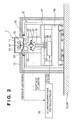
- Fig. 2 shows an exposure apparatus according to the second embodiment of the present invention.
- the same constituent elements as those of the first embodiment are denoted by the same reference numerals as in the first embodiment, and a detailed description thereof will be omitted.
- a light source position sensor 23 transmits a measurement signal to a collimator/wafer-stage position controller 25.
- the collimator/wafer-stage position controller 25 controls the position and attitude of a collimator 21 in accordance with the measured position of a light source 12, while correcting alignment of a mask 31 and wafer 32.
- X-rays are emitted, and the intensity distribution within the exposure field is measured by an X-ray intensity sensor 33 on a wafer stage 34.
- Intensity distribution measurement is repeatedly performed by sequentially changing the position and attitude of the collimator 21.
- the relationship between the intensity distribution within the exposure field and the attitude and position of the collimator 21 is stored in the collimator/wafer-stage position controller 25.
- the collimator/wafer-stage position controller 25 outputs commands to actuators 22 in order to perform position control such that the collimator 21 is positioned with such position and attitude that the intensity within the exposure field becomes uniform. This position of the collimator 21 is determined as the initial position.
- a change in exposure optical axis which takes place when the position of the collimator 21 is changed is also measured.
- the optical axis is measured by setting a pinhole at the mask position and measuring the position of exposure light passing through the pinhole with the X-ray intensity sensor 33.
- the relationship between the exposure optical axis and the position and attitude of the collimator 21 is also stored in the collimator/wafer-stage position controller 25 in the same as the intensity distribution is.
- the light source position sensor 23 constantly measures the position of the light source 12, and the collimator/wafer-stage position controller 25 controls the position and attitude of the collimator 21 on the basis of the data of the intensity distribution measured in advance described above, so that the intensity distribution of the exposure light within the exposure field becomes uniform. Furthermore, the collimator/wafer-stage position controller 25 calculates a change in optical axis on the basis of the data on the change of the exposure optical axis measured in advance, and corrects the wafer position such that the transfer error of the mask pattern onto the wafer surface, which occurs upon a change in optical axis, is corrected. For example, when the change in optical axis is 1 mrad and the exposure gap between the mask and wafer is 15 ⁇ m, correction of 15 nm is performed.
- the wafer stage 34 repeats stepping to expose the entire wafer 32. Each time the wafer stage 34 is stepped, it repeats acceleration and deceleration. Thus, a reaction force is generated to swing a main body 2, thus changing the positions of the light source 12 and main body 2 relative to each other. As the light source position sensor 23 is fixed on the main body 2 as described above, it measures the positions of the light source 12 and mask 31 relative to each other. By controlling the attitude of the collimator 21, exposure can be performed with illumination light having a uniform intensity distribution regardless of the attitude of the main body 2. Hence, stepping need not wait until the main body 2 is restored to its initial attitude.
- the wafer 32 can be exposed within a shorter period of time without decreasing the line width performance, so that the throughput can be improved. Even when a change occurs in the exposure optical axis due to the position and attitude of the collimator 21, if positioning of the wafer stage is corrected, the overlay accuracy is not decreased.
- the positions of the light source 12 and main body 2 (collimator 21) relative to each other are changed by an external temperature change or the like.
- the position of the collimator 21 can always be controlled with respect to the position of the light source 12 such that the intensity distribution becomes uniform within the exposure field, thereby maintaining the resolution performance. Even when a change occurs in the exposure optical axis due to the position and attitude of the collimator 21, if positioning of the wafer stage 34 is corrected, the overlay accuracy is not decreased.
- the light source position sensor 23 measures the position of the light source 12 by sensing visible light generated by the light source 12. If the position of the light source 12 is measured by any other means, no problem arises. In the description, an expression "the intensity becomes uniform" is employed. Note that the intensity need not be strictly uniform, but the intensity distribution must fall within an allowable range.
- semiconductor device semiconductor chip of IC, LSI or the like, a liquid crystal panel, a CCD, a thin film magnetic head, a micromachine etc.
- the system performs maintenance services such as trouble shooting, periodical maintenance or software delivery for fabrication apparatuses installed in a semiconductor manufacturing factory, by utilizing a computer network outside the fabrication factory.
- Fig. 4 shows the entire system cut out from an angle.
- numeral 1101 denotes the office of a vendor (apparatus maker) of semiconductor device fabrication apparatuses.
- semiconductor fabrication apparatuses apparatuses in the semiconductor fabrication factory for various processes such as preprocess apparatuses (lithography apparatuses including an exposure apparatus, a resist processing apparatus and an etching apparatus, a heat processing apparatus, a film forming apparatus, a smoothing apparatus and the like) and postprocess apparatuses (an assembly apparatus, an inspection apparatus and the like) are used.
- the office 1101 has a host management system 1108 to provide a maintenance database for the fabrication apparatus, plural operation terminal computers 1110, and a local area network (LAN) 1109 connecting them to construct an Intranet or the like.
- the host management system 1108 has a gateway for connection between the LAN 1109 and the Internet 1105 as an external network and a security function to limit access from the outside.
- numerals 1102 to 1104 denote fabrication factories of semiconductor makers as users of the fabrication apparatuses.
- the fabrication factories 1102 to 1104 may belong to different makers or may belong to the same maker (e.g., preprocess factories and postprocess factories).
- the respective factories 1102 to 1104 are provided with plural fabrication apparatuses 1106, a local area network (LAN) 1111 connecting the apparatuses to construct an Intranet or the like, and a host management system 1107 as a monitoring apparatus to monitor operating statuses of the respective fabrication apparatuses 1106.
- the host management system 1107 provided in the respective factories 1102 to 1104 has a gateway for connection between the LAN 1111 and the Internet 1105 as the external network.
- the host management system 1108 on the vendor side can be accessed from the LAN 1111 in the respective factories via the Internet 1105, and only limited user(s) can access the system by the security function of the host management system 1108. More particularly, status information indicating the operating statuses of the respective fabrication apparatuses 1106 (e.g. problem of fabrication apparatus having trouble) is notified from the factory side to the vendor side via the Internet 1105, and maintenance information such as response information to the notification (e.g. information indicating measure against the trouble, or remedy software or data), latest software, help information and the like is received from the vendor side via the Internet.
- status information indicating the operating statuses of the respective fabrication apparatuses 1106 e.g. problem of fabrication apparatus having trouble
- maintenance information such as response information to the notification (e.g. information indicating measure against the trouble, or remedy software or data), latest software, help information and the like is received from the vendor side via the Internet.
- the data communication between the respective factories 1102 to 1104 and the vendor 1101 and data communication in the LAN 1111 of the respective factories are performed by using a general communication protocol (TCP/IP).
- TCP/IP general communication protocol
- the external network a private-line network (ISDN or the like) with high security against access from outsiders may be used in place of the Internet.
- the host management system is not limited to that provided by the vendor, but a database constructed by the user may be provided on the external network, to provide the plural user factories with access to the database.
- Fig. 5 is a conceptual diagram showing the entire system of the present embodiment cut out from another angle different from that in Fig. 4.
- the plural user factories respectively having fabrication apparatuses and the management system of the apparatus vendor are connected via the external network, and data communication is performed for production management for the respective factories and transmission of information on at least one fabrication apparatus.
- a factory having fabrication apparatuses of plural vendors is connected with management systems of the respective vendors of the fabrication apparatuses via the external network, and data communication is performed for transmission of maintenance information for the respective fabrication apparatuses.
- numeral 1201 denotes a fabrication factory of fabrication apparatus user (semiconductor device maker).
- Fig. 5 shows only the fabrication factory 1201, however, actually plural factories construct the network.
- the respective apparatuses of the factory are connected with each other by a LAN 1206 to construct an Intranet, and a host management system 1205 performs operation management of the fabrication line.
- the respective offices of vendors (apparatus makers), an exposure apparatus maker 1210, a resist processing apparatus maker 1220, a film forming apparatus maker 1230 have host management systems 1211, 1221 and 1231 for remote maintenance for the apparatuses, and as described above, the systems have the maintenance database and the gateway for connection to the external network.
- the host management system 1205 for management of the respective apparatuses in the user fabrication factory is connected with the respective vendor management systems 1211, 1221 and 1231 via the Internet or private-line network as an external network 1200.
- the trouble can be quickly removed by receiving the remote maintenance service from the vendor of the apparatus via the Internet 1200, thus the stoppage of the fabrication line can be minimized.
- the respective fabrication apparatuses installed in the semiconductor fabrication factory have a display, a network interface and a computer to execute network access software stored in a memory and device operation software.
- a memory an internal memory, a hard disk or a network file server may be used.
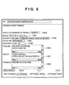
- the network access software including a specialized or general web browser, provides a user interface screen image as shown in Fig. 6 on the display.
- An operator who manages the fabrication apparatuses in the factory checks the screen image and inputs information of the fabrication apparatus, a model 1401, a serial number 1402, a trouble case name 1403, a date of occurrence of trouble 1404, an emergency level 1405, a problem 1406, a remedy 1407 and a progress 1408, into input fields on the screen image.
- the input information is transmitted to the maintenance database via the Internet, and appropriate maintenance information as a result is returned from the maintenance database and provided on the display.
- the user interface provided by the web browser realizes hyper link functions 1410 to 1412 as shown in the figure, and the operator accesses more detailed information of the respective items, downloads latest version software to be used in the fabrication apparatus from a software library presented by the vendor, and downloads operation guidance (help information) for the operator's reference.
- the maintenance information provided from the maintenance database includes the information on the above-described present invention, and the software library provides latest version software to realize the present invention.
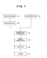
- Fig. 7 shows a flow of the entire semiconductor fabrication process.
- step S1 circuit designing
- step S2 mask fabrication
- step S3 wafer fabrication
- step S4 wafer process
- preprocess the above mask and wafer are used.
- An actual circuit is formed on the wafer by lithography.
- step S5 assembly
- the postprocess includes processing such as an assembly process (dicing and bonding) and a packaging process (chip sealing).
- processing such as an assembly process (dicing and bonding) and a packaging process (chip sealing).
- inspections such as an operation test and a durability test are performed on the semiconductor device assembled at step S5.
- the semiconductor device is completed through these processes, and it is shipped (step S7).
- the preprocess and the postprocess are independently performed in specialized factories, and maintenance is made for these factories by the above-described remote maintenance system. Further, data communication is performed for production management and/or apparatus maintenance between the preprocess factory and the postprocess factory via the Internet or private-line network.
- Fig. 8 shows a more detailed flow of the wafer process.
- step S11 oxidation
- step S12 CVD
- step S13 electrode formation
- step S14 ion implantation
- ions are injected into the wafer.
- step S15 resist processing
- step S16 exposure
- step S17 development
- step S18 etching
- step S19 resist stripping
- the resist unnecessary after the etching is removed.
Landscapes
- Physics & Mathematics (AREA)
- General Physics & Mathematics (AREA)
- Exposure And Positioning Against Photoresist Photosensitive Materials (AREA)
- Exposure Of Semiconductors, Excluding Electron Or Ion Beam Exposure (AREA)
- Preparing Plates And Mask In Photomechanical Process (AREA)
Abstract
Description
At step S6 (inspection), inspections such as an operation test and a durability test are performed on the semiconductor device assembled at step S5. The semiconductor device is completed through these processes, and it is shipped (step S7). The preprocess and the postprocess are independently performed in specialized factories, and maintenance is made for these factories by the above-described remote maintenance system. Further, data communication is performed for production management and/or apparatus maintenance between the preprocess factory and the postprocess factory via the Internet or private-line network.
Claims (21)
- An exposure apparatus which has an illumination optical system for generating exposure light by setting to a desired state X-rays emitted from an X-ray source that generates X-rays, and transfers a mask pattern onto a substrate, characterized by comprising:a detection unit for detecting a position of the X-ray source relative to a mask; anda correction unit for correcting a position and attitude of the illumination optical system on the basis of a detection result obtained by said detection unit.
- The apparatus according to claim 1, characterized in that said correction unit performs correction such that an exposure intensity becomes uniform within a predetermined allowable range.
- The apparatus according to claim 1, characterized in that positions of the mask and substrate relative to each other are corrected on the basis of the detection result obtained by said detection unit.
- An apparatus according to any one of claims 1 to 3, characterized in that the exposure apparatus is a proximity X-ray exposure apparatus.
- An exposing method which uses an illumination optical system for generating exposure light by setting to a desired state X-rays emitted from an X-ray source that generates X-rays, and transfers a mask pattern onto a substrate, characterized by comprising the steps of:detecting a position of the X-ray source relative to a mask; andcorrecting a position and attitude of the illumination optical system on the basis of a detection result.
- The method according to claim 5, characterized in that correction is performed such that an exposure intensity becomes uniform within a predetermined allowable range.
- The method according to claim 5, characterized in that positions of the mask and substrate relative to each other are corrected on the basis of the detection result.
- The method according to any one of claims 5 to 7, characterized in that exposure is proximity X-ray exposure.
- A semiconductor device fabricating method characterized by having the steps of:setting a group of fabrication apparatuses for respective types of processes including the exposure apparatus according to any one of claims 1 to 4 at a semiconductor fabrication factory; andfabricating a semiconductor device in accordance with a plurality of processes by using the group of fabrication apparatuses.
- The method according to claim 9, characterized by further comprising the steps of:connecting the group of fabrication apparatuses to each other through a local area network, anddata-communicating information on at least one of the group of fabrication apparatuses between the local area network and an external network outside the semiconductor fabrication factory.
- The method according to claim 10, characterized in that maintenance information on the fabrication apparatuses is obtained through data communication by accessing a database provided by a vender or user of the exposure apparatus through the external network, or production management is performed by data communication with another semiconductor fabrication factory through the external network.
- A semiconductor fabrication factory characterized by comprising
a group of fabrication apparatuses for respective types of processes including the exposure apparatus according to any one of claims 1 to 4,
a local area network for connecting the group of fabrication apparatuses, and
a gateway for enabling access to an external network outside the factory from the local area network, wherein
data communication of information on at least one of the group of fabrication apparatuses is enabled. - A maintenance method for the exposure apparatus according to any one of claims 1 to 4 which is set on a semiconductor fabrication factory, characterized by comprising the steps of:providing, by a vender or user of the exposure apparatus, a maintenance database connected to an external network outside the semiconductor fabrication factory;allowing access to the maintenance database from inside the semiconductor fabrication factory through the external network; andtransmitting maintenance information accumulated in the maintenance database to the semiconductor fabrication factory through the external network.
- The exposure apparatus according to any one of claims 1 to 4, characterized in that
the exposure apparatus further comprises a display, a network interface, and a computer for performing network software, and
data communication of maintenance information on the exposure apparatus through a computer network is enabled. - The exposure apparatus according to claim 14,
characterized in that
the network software provides a user interface for accessing a maintenance database, connected to an external network outside a factory where the exposure apparatus is set and provided by a vender or user of the exposure apparatus, on the display, so information can be obtained from the database through the external network. - Apparatus for exposing a substrate to a pattern of X-rays in the manufacture of a semiconductor device, the apparatus comprising:characterised by:an X-ray source (12);mask holding means for holding a mask (31) bearing a pattern;substrate holding means for holding the substrate (32); andan optical system (21) for exposing a substrate held by the substrate holding means with X-rays from the X-ray source via a mask held by the mask holding means,detection means (23) for detecting the position and/or movement of the X-ray source (12); andadjustment means (22) for adjusting the optical system (21) in response to detected movement, or change in the detected position, of the X-ray source.
- Apparatus according to claim 16 in which the adjustment means (22) is arranged to adjust the position and/or orientation at least a part of the optical system.
- Apparatus according to claim 16 or claim 17 comprising means for adjusting the relative positions of the mask (31) and the substrate (32) in response to adjustment of the optical system and/or detected movement or detected change in the position of the X-ray source.
- A method of exposing a substrate to a pattern of X-rays in the manufacture of a semiconductor device, comprising exposing the substrate to X-rays from an X-ray source through an optical system and a mask bearing a pattern,
characterised by detecting movement, or changes in the position, of the X-ray source, and adjusting the optical system in response thereto. - A method according to claim 19 in which the step of adjusting the optical system comprises adjusting the position and/or orientation of at least a part of the optical system.
- A method according to claim 19 or claim 20 which comprises adjusting the relative positions of the mask and the substrate in response to adjustment of the optical system and/or in response to detected movement or detected change in the position of the X-ray source.
Applications Claiming Priority (2)
| Application Number | Priority Date | Filing Date | Title |
|---|---|---|---|
| JP2001246214A JP2003059801A (en) | 2001-08-14 | 2001-08-14 | Exposure apparatus and exposure method |
| JP2001246214 | 2001-08-14 |
Publications (2)
| Publication Number | Publication Date |
|---|---|
| EP1286220A2 true EP1286220A2 (en) | 2003-02-26 |
| EP1286220A3 EP1286220A3 (en) | 2005-02-16 |
Family
ID=19075821
Family Applications (1)
| Application Number | Title | Priority Date | Filing Date |
|---|---|---|---|
| EP02255625A Withdrawn EP1286220A3 (en) | 2001-08-14 | 2002-08-13 | Exposure apparatus and exposing method |
Country Status (3)
| Country | Link |
|---|---|
| US (1) | US6754303B2 (en) |
| EP (1) | EP1286220A3 (en) |
| JP (1) | JP2003059801A (en) |
Families Citing this family (11)
| Publication number | Priority date | Publication date | Assignee | Title |
|---|---|---|---|---|
| JP2004047517A (en) * | 2002-07-08 | 2004-02-12 | Canon Inc | Radiation generation apparatus, radiation generation method, exposure apparatus and exposure method |
| JP4164414B2 (en) * | 2003-06-19 | 2008-10-15 | キヤノン株式会社 | Stage equipment |
| JP2005158926A (en) * | 2003-11-25 | 2005-06-16 | Canon Inc | Load lock device and method |
| JP4478440B2 (en) * | 2003-12-02 | 2010-06-09 | キヤノン株式会社 | Load lock device and method |
| JP2006165371A (en) * | 2004-12-09 | 2006-06-22 | Canon Inc | Transfer apparatus and device manufacturing method |
| CN1888977B (en) * | 2005-06-29 | 2010-09-08 | Ge医疗系统环球技术有限公司 | X-ray photographic system |
| CN102543243B (en) | 2010-12-28 | 2016-07-13 | Ge医疗系统环球技术有限公司 | Integrated capillary type parallel X-ray focusing lens |
| CN102735612A (en) * | 2011-04-02 | 2012-10-17 | 北京神农谷科技有限公司 | Light source position detection and positioning system |
| TWI679491B (en) | 2014-11-17 | 2019-12-11 | 荷蘭商Asml荷蘭公司 | Mask assembly suitable for use in a lithographic process |
| JP6278427B1 (en) * | 2017-01-05 | 2018-02-14 | レーザーテック株式会社 | Optical device and vibration isolation method |
| JP7168620B2 (en) * | 2020-08-26 | 2022-11-09 | MONET Technologies株式会社 | vehicle |
Family Cites Families (15)
| Publication number | Priority date | Publication date | Assignee | Title |
|---|---|---|---|---|
| US4896341A (en) | 1984-11-08 | 1990-01-23 | Hampshire Instruments, Inc. | Long life X-ray source target |
| DE3712049A1 (en) | 1986-04-10 | 1987-11-12 | Canon Kk | X-RAY EXPOSURE DEVICE |
| US4803712A (en) * | 1987-01-20 | 1989-02-07 | Hitachi, Ltd. | X-ray exposure system |
| DE69030348T2 (en) * | 1989-10-03 | 1997-09-04 | Canon K.K., Tokio/Tokyo | Exposure device |
| US5177774A (en) | 1991-08-23 | 1993-01-05 | Trustees Of Princeton University | Reflection soft X-ray microscope and method |
| JP3446287B2 (en) * | 1994-03-15 | 2003-09-16 | 富士通株式会社 | Reduction projection exposure apparatus and optical axis shift correction method |
| US5835560A (en) | 1994-05-24 | 1998-11-10 | Canon Kabushiki Kaisha | Exposure apparatus |
| US5453001A (en) | 1994-07-12 | 1995-09-26 | Huang; Kuo-Wen | Molding tool with blowing device |
| JP3278317B2 (en) | 1995-03-24 | 2002-04-30 | キヤノン株式会社 | Exposure apparatus and device manufacturing method |
| JP3255849B2 (en) | 1996-07-19 | 2002-02-12 | キヤノン株式会社 | Exposure equipment |
| JP3450622B2 (en) | 1996-07-19 | 2003-09-29 | キヤノン株式会社 | Exposure apparatus and device manufacturing method using the same |
| JP3450648B2 (en) | 1997-05-09 | 2003-09-29 | キヤノン株式会社 | Magnification correction apparatus, X-ray exposure apparatus equipped with magnification correction apparatus, and device manufacturing method |
| JP2000100685A (en) * | 1998-09-17 | 2000-04-07 | Nikon Corp | Exposure apparatus and exposure method using the apparatus |
| JP2001332472A (en) * | 2000-05-19 | 2001-11-30 | Canon Inc | X-ray exposure equipment |
| EP1174769B1 (en) * | 2000-07-10 | 2006-12-13 | ASML Netherlands B.V. | Lithographic projection apparatus and lithographic device manufacturing method |
-
2001
- 2001-08-14 JP JP2001246214A patent/JP2003059801A/en not_active Withdrawn
-
2002
- 2002-08-09 US US10/214,605 patent/US6754303B2/en not_active Expired - Fee Related
- 2002-08-13 EP EP02255625A patent/EP1286220A3/en not_active Withdrawn
Also Published As
| Publication number | Publication date |
|---|---|
| JP2003059801A (en) | 2003-02-28 |
| EP1286220A3 (en) | 2005-02-16 |
| US20030035508A1 (en) | 2003-02-20 |
| US6754303B2 (en) | 2004-06-22 |
Similar Documents
| Publication | Publication Date | Title |
|---|---|---|
| US6891175B2 (en) | Exposure apparatus and device manufacturing method using the same | |
| US7067826B2 (en) | Position detection method and apparatus | |
| JP2003068600A (en) | Exposure apparatus and substrate chuck cooling method | |
| US20030179377A1 (en) | Mirror device, mirror adjustment method, exposure apparatus, exposure method, and semiconductor device manufacturing method | |
| US6754303B2 (en) | Exposure apparatus and exposing method | |
| US6704093B2 (en) | Scanning exposure apparatus, scanning exposure method, and device manufacturing method | |
| JP2002367886A (en) | Exposure apparatus optimally adjusted by linear programming and adjustment method thereof | |
| US20210149309A1 (en) | Position measurement of optical elements in a lithographic apparatus | |
| JP2001284210A (en) | Exposure apparatus, device manufacturing method, semiconductor manufacturing factory, and maintenance method of exposure apparatus | |
| US7876419B2 (en) | Exposure apparatus and device manufacturing method | |
| US6864953B2 (en) | Exposure apparatus, device manufacturing method, semiconductor manufacturing plant and method of maintaining exposure apparatus | |
| US6754302B2 (en) | X-ray exposure apparatus | |
| US20020071106A1 (en) | Exposure apparatus and method | |
| JP2005322720A (en) | Stage control apparatus and method, exposure apparatus and method, and device manufacturing method | |
| JP2002359178A (en) | Projection exposure method and projection exposure apparatus | |
| US6646714B2 (en) | Exposure apparatus, imaging performance measurement method, device manufacturing method, semiconductor manufacturing factory, and exposure apparatus maintenance method | |
| JP2003142365A (en) | Exposure apparatus and exposure method | |
| JP2001297961A (en) | Exposure equipment | |
| JP2005136326A (en) | Apparatus state prediction apparatus and method, and exposure apparatus management system | |
| JP4817545B2 (en) | Exposure apparatus and device manufacturing method | |
| JP2001284223A (en) | Exposure equipment | |
| JP3337951B2 (en) | Projection exposure apparatus and method | |
| US6160865A (en) | X-ray exposure apparatus with synchrotron radiation intensity measurement | |
| JP2000331921A (en) | Exposure apparatus, exposure apparatus system, and device manufacturing method | |
| JP4881484B2 (en) | Exposure apparatus and device manufacturing method |
Legal Events
| Date | Code | Title | Description |
|---|---|---|---|
| PUAI | Public reference made under article 153(3) epc to a published international application that has entered the european phase |
Free format text: ORIGINAL CODE: 0009012 |
|
| AK | Designated contracting states |
Kind code of ref document: A2 Designated state(s): AT BE BG CH CY CZ DE DK EE ES FI FR GB GR IE IT LI LU MC NL PT SE SK TR Designated state(s): AT BE BG CH CY CZ DE DK EE ES FI FR GB GR IE IT LI LU MC NL PT SE SK TR |
|
| AX | Request for extension of the european patent |
Extension state: AL LT LV MK RO SI |
|
| PUAL | Search report despatched |
Free format text: ORIGINAL CODE: 0009013 |
|
| AK | Designated contracting states |
Kind code of ref document: A3 Designated state(s): AT BE BG CH CY CZ DE DK EE ES FI FR GB GR IE IT LI LU MC NL PT SE SK TR |
|
| AX | Request for extension of the european patent |
Extension state: AL LT LV MK RO SI |
|
| 17P | Request for examination filed |
Effective date: 20050701 |
|
| AKX | Designation fees paid |
Designated state(s): AT BE BG CH CY CZ DE DK EE ES FI FR GB GR IE IT LI LU MC NL PT SE SK TR |
|
| 17Q | First examination report despatched |
Effective date: 20090825 |
|
| STAA | Information on the status of an ep patent application or granted ep patent |
Free format text: STATUS: THE APPLICATION HAS BEEN WITHDRAWN |
|
| 18W | Application withdrawn |
Effective date: 20091229 |