EP1284520A2 - Cell plate structure for solid electrolyte fuel cell, solid electrolyte fuel cell and related manufacturing method - Google Patents
Cell plate structure for solid electrolyte fuel cell, solid electrolyte fuel cell and related manufacturing method Download PDFInfo
- Publication number
- EP1284520A2 EP1284520A2 EP02017945A EP02017945A EP1284520A2 EP 1284520 A2 EP1284520 A2 EP 1284520A2 EP 02017945 A EP02017945 A EP 02017945A EP 02017945 A EP02017945 A EP 02017945A EP 1284520 A2 EP1284520 A2 EP 1284520A2
- Authority
- EP
- European Patent Office
- Prior art keywords
- electrode layer
- lower electrode
- upper electrode
- layer
- substance
- Prior art date
- Legal status (The legal status is an assumption and is not a legal conclusion. Google has not performed a legal analysis and makes no representation as to the accuracy of the status listed.)
- Granted
Links
Images


Classifications
-
- H—ELECTRICITY
- H01—ELECTRIC ELEMENTS
- H01M—PROCESSES OR MEANS, e.g. BATTERIES, FOR THE DIRECT CONVERSION OF CHEMICAL ENERGY INTO ELECTRICAL ENERGY
- H01M8/00—Fuel cells; Manufacture thereof
- H01M8/10—Fuel cells with solid electrolytes
- H01M8/12—Fuel cells with solid electrolytes operating at high temperature, e.g. with stabilised ZrO2 electrolyte
- H01M8/1213—Fuel cells with solid electrolytes operating at high temperature, e.g. with stabilised ZrO2 electrolyte characterised by the electrode/electrolyte combination or the supporting material
- H01M8/1226—Fuel cells with solid electrolytes operating at high temperature, e.g. with stabilised ZrO2 electrolyte characterised by the electrode/electrolyte combination or the supporting material characterised by the supporting layer
-
- H—ELECTRICITY
- H01—ELECTRIC ELEMENTS
- H01M—PROCESSES OR MEANS, e.g. BATTERIES, FOR THE DIRECT CONVERSION OF CHEMICAL ENERGY INTO ELECTRICAL ENERGY
- H01M4/00—Electrodes
- H01M4/86—Inert electrodes with catalytic activity, e.g. for fuel cells
- H01M4/88—Processes of manufacture
- H01M4/8803—Supports for the deposition of the catalytic active composition
- H01M4/881—Electrolytic membranes
-
- H—ELECTRICITY
- H01—ELECTRIC ELEMENTS
- H01M—PROCESSES OR MEANS, e.g. BATTERIES, FOR THE DIRECT CONVERSION OF CHEMICAL ENERGY INTO ELECTRICAL ENERGY
- H01M4/00—Electrodes
- H01M4/86—Inert electrodes with catalytic activity, e.g. for fuel cells
- H01M4/88—Processes of manufacture
- H01M4/8878—Treatment steps after deposition of the catalytic active composition or after shaping of the electrode being free-standing body
- H01M4/8882—Heat treatment, e.g. drying, baking
- H01M4/8885—Sintering or firing
- H01M4/8889—Cosintering or cofiring of a catalytic active layer with another type of layer
-
- H—ELECTRICITY
- H01—ELECTRIC ELEMENTS
- H01M—PROCESSES OR MEANS, e.g. BATTERIES, FOR THE DIRECT CONVERSION OF CHEMICAL ENERGY INTO ELECTRICAL ENERGY
- H01M8/00—Fuel cells; Manufacture thereof
- H01M8/10—Fuel cells with solid electrolytes
- H01M8/12—Fuel cells with solid electrolytes operating at high temperature, e.g. with stabilised ZrO2 electrolyte
- H01M8/1213—Fuel cells with solid electrolytes operating at high temperature, e.g. with stabilised ZrO2 electrolyte characterised by the electrode/electrolyte combination or the supporting material
- H01M8/122—Corrugated, curved or wave-shaped MEA
-
- H—ELECTRICITY
- H01—ELECTRIC ELEMENTS
- H01M—PROCESSES OR MEANS, e.g. BATTERIES, FOR THE DIRECT CONVERSION OF CHEMICAL ENERGY INTO ELECTRICAL ENERGY
- H01M8/00—Fuel cells; Manufacture thereof
- H01M8/10—Fuel cells with solid electrolytes
- H01M8/12—Fuel cells with solid electrolytes operating at high temperature, e.g. with stabilised ZrO2 electrolyte
- H01M8/124—Fuel cells with solid electrolytes operating at high temperature, e.g. with stabilised ZrO2 electrolyte characterised by the process of manufacturing or by the material of the electrolyte
-
- H—ELECTRICITY
- H01—ELECTRIC ELEMENTS
- H01M—PROCESSES OR MEANS, e.g. BATTERIES, FOR THE DIRECT CONVERSION OF CHEMICAL ENERGY INTO ELECTRICAL ENERGY
- H01M8/00—Fuel cells; Manufacture thereof
- H01M8/10—Fuel cells with solid electrolytes
- H01M8/12—Fuel cells with solid electrolytes operating at high temperature, e.g. with stabilised ZrO2 electrolyte
- H01M8/1286—Fuel cells applied on a support, e.g. miniature fuel cells deposited on silica supports
-
- Y—GENERAL TAGGING OF NEW TECHNOLOGICAL DEVELOPMENTS; GENERAL TAGGING OF CROSS-SECTIONAL TECHNOLOGIES SPANNING OVER SEVERAL SECTIONS OF THE IPC; TECHNICAL SUBJECTS COVERED BY FORMER USPC CROSS-REFERENCE ART COLLECTIONS [XRACs] AND DIGESTS
- Y02—TECHNOLOGIES OR APPLICATIONS FOR MITIGATION OR ADAPTATION AGAINST CLIMATE CHANGE
- Y02E—REDUCTION OF GREENHOUSE GAS [GHG] EMISSIONS, RELATED TO ENERGY GENERATION, TRANSMISSION OR DISTRIBUTION
- Y02E60/00—Enabling technologies; Technologies with a potential or indirect contribution to GHG emissions mitigation
- Y02E60/30—Hydrogen technology
- Y02E60/50—Fuel cells
-
- Y—GENERAL TAGGING OF NEW TECHNOLOGICAL DEVELOPMENTS; GENERAL TAGGING OF CROSS-SECTIONAL TECHNOLOGIES SPANNING OVER SEVERAL SECTIONS OF THE IPC; TECHNICAL SUBJECTS COVERED BY FORMER USPC CROSS-REFERENCE ART COLLECTIONS [XRACs] AND DIGESTS
- Y02—TECHNOLOGIES OR APPLICATIONS FOR MITIGATION OR ADAPTATION AGAINST CLIMATE CHANGE
- Y02P—CLIMATE CHANGE MITIGATION TECHNOLOGIES IN THE PRODUCTION OR PROCESSING OF GOODS
- Y02P70/00—Climate change mitigation technologies in the production process for final industrial or consumer products
- Y02P70/50—Manufacturing or production processes characterised by the final manufactured product
Definitions
- the present invention relates to a cell plate structure for a solid electrolyte fuel cell, a solid electrolyte fuel cell and a related manufacturing method thereof and, more particularly, to a cell plate structure for a solid electrolyte fuel cell, which uses a solid electrolyte to obtain electrical energy due to an electro-chemical reaction, a solid electrolyte fuel cell using such a cell plate structure and a related manufacturing method thereof.
- solid oxide electrolyte type fuel cell employs electrolyte composed of an oxide ion conductivity type solid electrolyte such as yttria-stabilized zirconia.
- both surfaces (front and rear surfaces) of the electrolyte layer are formed with porous electrodes to allow the solid electrolyte to serve as a partition wall wherein one electrode is supplied with fuel gas such as hydrogen or hydrocarbon and the other electrode is supplied with oxidizing gas such as air or oxygen to permit the fuel cell to generally operate at a temperature about 1000°C for obtaining electrical energy.
- fuel gas such as hydrogen or hydrocarbon
- oxidizing gas such as air or oxygen
- the solid electrolyte of such an SOFC has an electrical conductivity, lower than that of the electrolyte of a phosphoric acid type fuel cell or a molten carbonate type fuel cell approximately by one digit number.
- electrical resistance of the electrolyte portion forms a loss in electric power generation output.
- the electrolyte layer it is required for the electrolyte layer to have a surface area greater in value to some extent in order to enhance various functions of the fuel cell and, hence, the SOFC employs a cell structure (unit cell structure) wherein the electrolyte layer is formed on a supporting member having a mechanical strength.
- Japanese Patent Application Laid-Open Publication No. H8-64216 discloses a fuel cell that attempts to form an electrolyte layer in a thin film and, more particularly, discloses a structure wherein a supporting substrate is formed with a large number of small opening portions each of which accommodates the cell plate structure structured to have a fuel electrode layer, an electrolyte layer and an air electrode layer deposited in three film layers, and a separator plate formed with flow passages, with the cell plate and the separator plate being alternately laminated.
- a non-porous silicon (Si) wafer as a supporting substrate which is formed with various elementary layers in film shapes, providing a capability of forming the electrolyte layer with a thickness in the order of approximately 2 ⁇ m.
- an electrolyte layer composed of stabilized zirconia formed in a single crystal film is formed on a Si substrate or a Si substrate formed with an oriented cerium oxide (CeO 2 ) thereon.
- the electrolyte portion in order to improve the electric power output density, it is certainly required for the electrolyte portion to be formed in the thin film so as to lower the electrical conductivity of the electrolyte portion and, on the other hand, it is important for the electrolyte layer to ensure an adequate dense property because the SOFC internally has the electrolyte layer as the partition wall for fuel gas and air. For instance, the presence of a leakage of fuel gas and air even in a small amount due to a pin hole formed in the electrolyte layer causes such gases to directly react with one another, resulting in a loss of electric power generating output. From such viewpoints, even in the presence of the non-porous supporting substrate or the porous supporting substrate, it is importantly conceivable that the supporting substrate is formed with a dense electrolyte film.
- such a structure concerns a feature wherein the electrolyte layer is formed on the substrate having an excellent flatness with non-porous property and has a dense thin film in the order of less than several micrometers.
- Another feature resides in that the electrolyte layer and both electrode layers are entirely formed on a single sheet of Si substrate having a large number of small opening portions and the electrolyte film is directly formed on the Si substrate in a single crystal film after removal of oxide film from the Si substrate.
- the lower electrode layer in order for the electrolyte layer to be formed in a thin film with a sufficient density, the lower electrode layer must be formed in a high flatness.
- the use of such a structure wherein the electrolyte layer is formed on the lower electrode layer having the high flatness results in an inability in enhancing adequate surface areas in the reaction interfaces related to the three phases involving the electrolyte layer and the both electrode layers, at which an actual cell reaction takes place, and reaction gases such as air and fuel gas.
- reaction gases such as air and fuel gas.
- the reacting gas is supplied to the interface between the lower electrode layer and the electrolyte layer behind the dense electrode layer having the high flatness, i.e. behind the lower electrode layer.
- a difficulty is encountered in supplying sufficient amounts of reacting gases necessary for reaction.
- the present invention has been completed upon considerable research and development work conducted by the present inventors, in view of the above studies, based on a newly obtained knowledge as to such a step in which especially, when forming at least one of electrode layers, a substance to be removed in a post-treatment is contained in the at least one of electrode layers and then the included substance is removed from the at least one of electrolyte layers in the post-treatment.
- SOFC cell plate structure as the case may be
- a cell plate structure for an SOFC comprises: a lower electrode layer; an upper electrode layer provided in opposition to the lower electrode layer; a solid electrolyte layer provided between the lower electrode layer and the upper electrode layer; and an area provided in at least one of the lower electrode layer and the upper electrode layer.
- the area has a portion which is formed by removing a substance, contained in the at least one of the lower electrode layer and the upper electrode layer during formation thereof, after the at least one of the lower electrode layer and the upper electrode layer has been formed.
- a method of manufacturing a cell plate structure for an SOFC comprises: forming a lower electrode layer; forming an upper electrode layer, the lower electrode layer and the upper electrode layer being provided in opposition to the lower electrode layer; forming a solid electrolyte layer, which is provided between the lower electrode layer and the upper electrode layer; allowing a substance to be contained in at least one of the lower electrode layer and the upper electrode layer; and executing a post-treatment by removing the substance, contained in the at least of the lower electrode layer and the upper electrode layer during formation thereof, after the at least one of the lower electrode layer and the upper electrode layer has been formed, to make the at least one of the lower electrode layer and the upper electrode layer porous.
- a cell plate structure for an SOFC comprises: a cell plate structure; and a pair of separators between which the cell plate structure is provided and which have gas flow passages.
- the cell plate structure is provided with: a lower electrode layer; an upper electrode layer provided in opposition to the lower electrode layer; a solid electrolyte layer provided between the lower electrode layer and the upper electrode layer; and an area provided in at least one of the lower electrode layer and the upper electrode layer.
- the area has a portion which is formed by removing a substance, contained in the at least one of the lower electrode layer and the upper electrode layer during formation thereof, after the at least one of the lower electrode layer and the upper electrode layer has been formed.
- a gas supplied through the gas flow passages is supplied toward the solid electrolyte layer through such a portion.
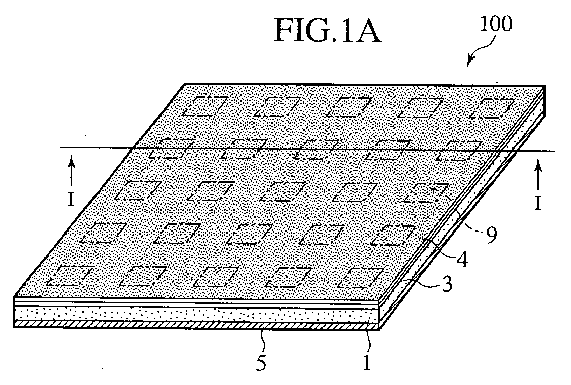
- Fig. 1A is a schematic perspective view showing an external structure of the SOFC cell plate structure of the preferred embodiment
- Fig. 1B is a cross sectional view taken on line I-I of Fig. 1A
- Fig. 1C is an enlarged cross sectional view illustrating a cell portion, shown in Fig. 1B, in an enlarged scale.
- the SOFC cell plate structure 100 is comprised of a silicon substrate 1 formed in a square shape with the width of 10 cm, with cell portions 7 each having an opening formed in a square shape with the width of approximately 5 mm being formed in 5 x 5 pieces.
- the silicon substrate 1 has a surface formed with an insulation layer (insulation and stress relaxation layer) 2 and includes five pieces of opening portions 9.
- the surface of the silicon substrate 1 formed with the insulation layer 2 is formed with an electrolyte layer 3 and an upper electrode layer 4 so as to cover the opening portions 9.
- a rear surface of the silicon substrate 1 is formed with a lower electrode layer 5 such that a surface of the lower electrode layer 5 is held in direct contact with a rear surface of the electrolyte layer 3.
- both the upper electrode layer 4 and the lower electrode layer 5 are formed with a large number of pores 6 to have a porous property.
- a porous area A is formed as to the upper electrode layer 4 and the lower electrode layer 5.
- such pores 6 may be called as voids or the like and they may have sizes, profiles and distribution enough to allow reacting gas to be supplied to a so-called reaction interface.
- Figs. 2A, 2C, 2E, 3A, 3C and 3E are cross sectional views for principally showing the cell portion 7 of the SOFC cell plate structure 100 to sequentially illustrate such a fabrication process
- Figs. 2B, 2D, 2F, 3B, 3D and 3F are plan views corresponding to Figs. 2B, 2D, 2F, 3B, 3D and 3F, respectively.
- both surfaces at front and rear sides of the silicon substrate 1 are formed with silicon nitride layers to have a thickness in the order of approximately 2000 ⁇ by a reduced pressure CVD method, the layer at the front surface of which is used as the insulation layer 2.
- a desired patterned area of the silicon nitride layer formed on an entire area of the rear surface is subjected to exposure of light and then, the exposed, patterned area is removed, thereby forming a mask layer 8 that functions as a mask during a silicon etching step which will be described below in conjunction with the next fabrication step.
- the electrolyte layer 3 made of yttria stabilized zirconia (hereinafter referred to as YSZ) is deposited onto the insulation layer 2 with a thickness of approximately 2 ⁇ m by an RF sputtering method.
- the silicon etching step is conducted at a temperature of approximately 80°C using hydrazine, presenting a strong alkaline property, as silicon etching liquid to etch the silicon substrate 1, forming a substrate opening portion 9 at the rear surface side of the silicon substrate 1.
- the surface side of the silicon substrate 1 is formed with a so-called diaphragm composed of the insulation layer 2 made of the silicon nitride film and the electrolyte layer 3 made of YSZ.
- the rear surface side of the silicon substrate 1 is subjected to a chemical dry etching method using CF 4 and O 2 , thereby allowing the insulation layer 2, forming part of such diaphragm, and the mask layer 8 to be removed.
- the upper electrode layer 4 is formed on the surface of the silicon substrate 1 in a film of (La 1-x Sr x )CoO 3- ⁇ (hereinafter referred to as LSC) with a thickness in a range of approximately 500 nm so as to cover the electrolyte layer 3 by an RF sputtering method with the use of a deposition mask corresponding to a size of the electrolyte layer 3.
- LSC film of (La 1-x Sr x )CoO 3- ⁇
- the lower electrode layer 5 is formed on the rear surface of the silicon substrate 1 in a film of a cermet made of YSZ-NiO with a thickness in a range of approximately 500 nm so as to be held in contact with the rear surface of the electrolyte layer 3 by an RF sputtering method.
- an RF sputtering method When conducting such an RF sputtering method, the addition of carbon in both targets for the RF sputtering enables both the resulting upper electrode layer 4 and lower electrode layer 5 formed in the film shapes to contain carbon particles 10.
- a heat treatment is carried out at a temperature of approximately 1000°C in an atmosphere that causes oxidation of carbon to a sufficient extent or in an oxygen containing circumstance for compelling the carbon compounds to be oxidized to initiate gasification as CO 2 , resulting in the formation of a large number of pores 6 both in the upper electrode layer 4 and the lower electrode layer 5.
- the SOFC cell plate structure 100 it is possible for the SOFC cell plate structure 100 to be made of the cell portions 7 with a structure wherein the upper electrode layer 4 and the lower electrode layer 5 have respective insides formed with the pores 6 to present porous properties and wherein the lower electrode layer 5, the electrolyte layer 3 and the upper electrode layer 4 are sequentially formed on the surface side of the silicon substrate 1 in three layers.
- Fig. 4A is a plan view illustrating a separator
- Fig. 4B is an end view as viewed from a side of Fig. 4A
- Fig. 4C is an end view as viewed from a front of Fig. 4A.
- the separator S is prepared. While the separator S serves to allow the SOFC cell plate structures 100, formed in a manner set forth above, to be suitably stacked in a fuel cell stack, a description will be given to a structure of the unit cell for a convenience of simplification in description.
- the separator S includes a silicon plate in a rectangular shape with the width of 10 cm, with both surfaces being formed with gas flow passages G1 and G2 by cutting operations using a dicing saw. Also, the gas flow passages G1 and G2 extend so as to intersect with respect to one another in a so-called cross-flow type.
- two sheets of separators S are placed to be opposed to one another, between which the SOFC cell plate structure 100 is disposed to allow the upper separator S to be adhered to the upper electrode layer 4 of the SOFC cell plate structure 100 and the lower separator S to be adhered to the lower electrode layer 5. Also, electrical conductivities are enhanced between the upper separator S and the upper electrode layer 4 of the SOFC cell plate structure 100 and between the lower separator S and the lower electrode layer 5 of the SOFC cell plate structure 100, respectively.
- the unit cell 200 is fabricated to form a unitary structure wherein the unit cell is caught between the upper and lower separators S, S.
- the unit cell 200 fabricated in such a way as set forth above, is placed in an electric furnace at a furnace temperature of 700°C. Then, oxygen gas is supplied to the upper electrode layer 4 via the gas flow passages G2 of the upper separators S and hydrogen gas is supplied to the lower electrode layer 5 via the gas flow passages G1 of the lower separator S, with evaluation of an electric power generating characteristic of the unit cell being conducted. Upon evaluation, an open-circuit voltage appeared between the upper and lower separators S, S was 0.95V with a resulting maximum power output being 0.2W/cm 2 .
- the electrolyte layer 3 tends to have a defect-free thin film with a remarkably excellent film quality, with a resultant decrease in resistance in oxygen ion transference inside the electrolyte layer 3 that would otherwise causes deterioration in the electric power generating characteristic.
- the reacting gases can be supplied to the reaction interfaces defined by the upper electrode layer 4, the electrolyte 3 and the lower electrode layer 5 in an extremely preferable fashion in comparison with a case in which the reacting gases is supplied only through grain boundaries of the electrodes.
- effective surface areas of the reaction interfaces as to three phases of the electrolyte layer, the electrode layer and the reacting gases is remarkably increased, with a resultant significant increase in the electric power generating efficiency.
- the addition of carbon in the target of each of the electrode materials enables the upper electrode layer 4 and the lower electrode layer 5 to contain carbon particles once and the addition of the simple step of conducting the heat treatment in the oxidizing atmosphere enables the formation of the dense and desirable electrolyte layer 3 to be compatible with the formation of the porous upper electrode layer 4 and the porous lower electrode layer 5, thereby providing an excellent advantage in that the electric power generating efficiency is remarkably improved.
- the present invention is not limited thereto and it may be possible to adopt other film forming methods involving a co-sputtering method using dual targets one of which is an electrode material and the other of which is a material including carbon, a PVD method such as a vapor deposition method, an ion plating method and a laser abrasion method, a thermal spraying method, a paste coating method and a sol-gel method.
- a PVD method such as a vapor deposition method, an ion plating method and a laser abrasion method
- thermal spraying method a paste coating method and a sol-gel method.
- the present invention is not limited to carbon and may employ other substances, provided that such materials are oxidized and gasified due to a heat treatment in an oxidizing atmosphere, such as molybdenum, molybdenum compounds, tungsten and tungsten compounds.
- a post-treatment may involve a plasma treatment using CF 4 and O 2 , with substances to be contained including silicon, silicon nitride, molybdenum silicide, tungsten silicide, titanium, titanium nitride and titanium oxide that can be gasified and removed. Also, it is not objectionable for a post-treatment to involve a plasma treatment using CF 4 and H 2 , with substances to be contained including silicon oxide.
- the substance to be contained in the electrode layers may include silicon oxide that can be dissolved and removed by the hydrogen fluoride solution.
- the substance to be contained in the electrode layers may include silicon that can be dissolved and removed by the strong alkaline solution.
- a heat treatment may be conducted in a non-oxidizing atmosphere to grow up crystalline particles prior to conducting a heat treatment in an oxidizing atmosphere as a post-treatment, with the size of the pores 6 being controlled in the post-treatment.
- the present invention is not limited to particular sizes of the silicon substrate 1 and the film thickness of the layers to be formed and may take the form of any other dimensions if desired, with the number of cell portions 7 to be incorporated in the cell plate structure or fuel cell being not limited to a particular number of pieces.
- the present invention is not limited to particular materials of other component parts of the SOFC of the preferred embodiment.
- the electrolyte layer 3 may be composed of other material that has oxygen ion transfer property
- the upper electrode layer 4 may be composed of other material such as lanthanum-strontium-manganese oxide (LSM)
- the lower electrode material 5 may be composed of other material such as nickel or platinum.
- the second preferred embodiment has the same structure as the first preferred embodiment except for that all of the lower electrode layer 5, the electrolyte layer 3 and the upper electrode layer 4 are preliminarily laminated on the diaphragm composed of the silicon nitride film serving as the insulation layer 2, the layers of component part of the SOFC are laminated in a different order, with a substance to be contained in the upper electrode layer 4 and the lower electrode layer 5 once and arranged to contain silicon nitride that is different from the substance to be contained once in the electrode layers of the first preferred embodiment. Consequently, the second preferred embodiment is described in a suitably simplified manner with such differential points being focused, with like component parts bearing the same reference numerals as those used in the first preferred embodiment.
- Figs. 6A, 6C, 6E, 7A and 7C are cross sectional views principally showing a cell portion 7 of an SOFC cell plate structure 100 for sequentially illustrating a fabrication process of the manufacturing method of the SOFC cell plate structure of the presently filed preferred embodiment
- Figs. 6B, 6D, 6F, 7B and 7D are plan views corresponding to Figs. 6A, 6C, 6E, 7A and 7C, respectively.
- a silicon nitride film is formed on a surface of a silicon substrate 1 to have a thickness in the order of approximately 2000 ⁇ by a reduced pressure CVD method, thereby forming an insulation layer 2.
- a rear surface of the silicon substrate 1 is formed with a silicon nitride film, that serves as a mask layer 8 during a silicon etching step as will be described later, with a thickness in the order of approximately 2000 ⁇ by a reduced pressure CVD method.
- a desired area of the silicon nitride film is exposed to light and, then, the exposed area is removed, thereby completing the mask layer 8.
- the silicon etching step is conducted at a temperature of approximately 80°C using hydrazine as silicon etching liquid, forming a substrate opening portion 9 at the rear surface of the silicon substrate 1.
- the diaphragm of the insulation film 2 is formed on the front surface of the silicon substrate 1.
- the front surface of the silicon substrate 1 is formed with the cermet of YSZ-NiO with a thickness in the order of approximately 500 nm by an RF sputtering method, thereby forming a lower electrode layer 5.
- adding silicon nitride in the target to be sputter deposited allows the lower electrode 5 in the form of the film to contain silicon nitride particles 11.
- an electrolyte layer 3 composed of YSZ is formed on the lower electrode layer 5 and has a thickness of approximately 2 ⁇ m by an RF sputtering method.
- a film of LSC is formed on the electrolyte layer 3 to have a thickness of approximately 500 nm by an RF sputtering method, with a subsequent formation of an upper electrode layer 4.
- an upper electrode layer 4 also the addition of silicon nitride in the target to be sputter deposited allows the upper electrode layer 4 to be formed in a film containing silicon nitride particles 11.
- a chemical dry etching method using CF 4 and O 2 is conducted at the rear surface of the silicone substrate 1, thereby removing the silicon nitride film (insulation layer 2) and the mask layer 8 from the rear surface of the diaphragm portion. And, by presetting the treatment time period needed for such a chemical dry etching to be longer than the etching time period required for the silicon nitride film (insulation layer 2) for removing silicon nitride contained in the upper electrode layer 4 and the lower electrode layer 5, a large number of pores 6 are formed in the upper electrode layer 4 and the lower electrode layer 5.
- the upper electrode layer 4 and the lower electrode layer 5 are internally rendered to be porous such that the pores 6 are present, and the SOFC cell plate structure 100 is formed with the cell portions 7 each with a structure composed of three layers involving the lower electrode layer 5, the electrolyte layer 3 and the upper electrode layer 4 which are sequentially laminated on the front surface of the silicon substrate 1.
- an SOFC (unit cell) is prepared in the same manner as the first preferred embodiment to conduct evaluation of the electric power generating efficiency, with a similar result being obtained.
- preliminarily laminating all of the lower electrode layer 5, the electrolyte layer 3 and the upper electrode layer 4 on the diaphragm of the silicon nitride film and compelling the upper electrode layer 4 and the lower electrode layer 5 to contain silicon nitride that is the substance to be removed by the chemical dry etching method to remove the silicon nitride film provides a capability of forming the pores 6 in the upper electrode layer 4 and the lower electrode layer 5 to reliably have a desired porous quality therein without increasing the number of fabrication steps.
- the use of the technology for removing the silicon nitride film (insulation layer 2) by etching after forming the three layers, composed of the lower electrode layer 5, the electrolyte layer 3 and the upper electrode layer 4, on the diaphragm of the silicon nitride film (insulation layer 2) that is extremely strong in structure enables respective layers to be precluded from being damaged in the course of fabrication steps, resulting in an improvement in a production yield and reliability.
- the silicon substrate 1 is also etched by the chemical dry etching method with CF 4 and O 2 , the presence of the electrode with the thickness in the order of approximately 500 nm permits the silicon substrate 1 to be correspondingly cut away in a minute amount to preclude the same from being adversely affected in its function.
- silicon nitride is used as the substance to be contained in the upper electrode layer 4 and the lower electrode layer 5, of course, the present invention is not limited to such a substance and may utilize substances that react with and are gasified by plasma of CF 4 and O 2 during the chemical dry etching method.
- these substances may include silicon, molybdenum silicide, tungsten silicide, titanium, titanium nitride and titanium oxide.
- the upper electrode layer 4 and the lower electrode layer 5 may be similarly formed with the pores 6 to provide the porous properties, respectively, by changing the kind of gases to create plasma during such a chemical dry etching method and by permitting particular substance, to be etched by such plasma, to be contained in the electrodes.
- the heat treatment may be conducted at an appropriate condition once to grow up crystalline particles prior to the post-treatment and, subsequently, the post-treatment may be conducted so as to form the pores 6 in varying sizes.
- the third preferred embodiment has the same structure as the first preferred embodiment except for that all of the lower electrode layer 5, the electrolyte layer 3 and the upper electrode layer 4 are laminated on a silicon substrate 1 and subsequently the silicon substrate 1 is etched by silicon etching liquid to form pores 6 in the upper electrode layer 4 and the lower electrode laver 5, and that layers of the component parts of the SOFC are laminated in a different order and the pores 6 of the upper electrode layer 4 and the lower electrode layer 5 are formed in a different step. Consequently, the third preferred embodiment is described below in a suitably simplified manner with such differential points being focused, with like component parts bearing the same reference numerals as those used in the first preferred embodiment.
- Figs. 8A, 8C and 8E are cross sectional views principally showing a cell portion 7 of an SOFC cell plate structure 100 for sequentially illustrating a fabrication process of the manufacturing method of the SOFC cell plate structure of the presently filed preferred embodiment
- Figs. 8B, 8D and 8F are plan views corresponding to Figs. 8A, 8C and 8E, respectively.
- silicon nitride films are formed on both surfaces of a silicon substrate 1 to have a thickness in the order of approximately 2000 ⁇ by a reduced pressure CVD method, thereby forming an insulation layer 2 on the surface side while forming a mask layer 8 on the rear surface side to allow a silicon etching step as will be described later.
- a photo-lithography method and a chemical dry etching method using CF 4 and O 2 desired areas of the silicon nitride films formed on the surface and the rear surface of the silicon substrate 1 are exposed to light and, then, the exposed areas are removed, thereby forming the insulation layer 2 and the mask layer 8 on front and rear surfaces of the silicon substrate 1 in respective desired patterns.
- the surface of the silicon substrate 1 is formed with the cermet of YSZ-NiO with a thickness in the order of approximately 500 nm by an RF sputtering method, thereby forming a lower electrode layer 5.
- adding silicon in the target to be sputter deposited allows the lower electrode layer 5 to be formed in a film that contains silicon particles 12.
- the electrolyte layer 3 composed of YSZ is formed in a film on the lower electrode layer 5 and has a thickness of approximately 2 ⁇ m by an RF sputtering method while a film of LSC is formed on the electrolyte layer 3 as the upper electrode layer 4 with a thickness of approximately 500 nm by an RF sputtering method.
- the addition of silicon in the target to be sputter deposited allows the upper electrode layer 4 to be formed in the film containing silicon particles 12.
- the silicon etching step using hydrazine as silicon etching liquid is conducted at the rear surface of the silicone substrate 1 at a temperature of approximately 80°C, thereby forming a substrate opening portion 9.
- the silicon particles contained in the upper electrode layer 4 and the lower electrode layer 5 are etched at the same time that the silicon substrate 1 is etched with the silicon etching liquid, with a resultant formation of pores 6 in the upper electrode layer 4 and the lower electrode layer 5.
- the upper electrode layer 4 and the lower electrode layer 5 are internally rendered porous such that the pores 6 are present, and the SOFC cell plate structure 100 is formed with the cell portions 7 each with a structure composed of three layers involving the lower electrode layer 5, the electrolyte layer 3 and the upper electrode layer 4 which are sequentially laminated on the front surface of the silicon substrate 1.
- an SOFC (unit cell) is prepared in the same manner as the first preferred embodiment to conduct evaluation of the electric power generating efficiency, with a similar result being obtained.
- the presently filed preferred embodiment concerns a feature of laminating the lower electrode layer 5, the electrolyte layer 3 and the upper electrode layer 4 on the silicon substrate 1 in order and subsequently conducting the etching step of the silicon substrate 1 with the silicon etching liquid
- the presence of the upper electrode layer 4 and the lower electrode layer 5 preliminarily containing silicon to be subsequently removed during the silicon etching step provides a capability of forming the pores 6 in the upper electrode layer 4 and the lower electrode layer 5 using the silicon etching step without increasing the number of fabrication steps.
- silicon is used as the substance to be contained in the upper electrode layer 4 and the lower electrode layer 5, of course, the present invention is not limited to such a substance and may utilize other substances that are dissolved with the silicon etching liquid.
- the intrusion substance whose crystalline grows up due to a heat treatment allows the crystalline particles to be grown up once upon the heat treatment at an appropriate condition prior to a post-treatment and, subsequently, the post-treatment may be conducted so as to form the pores 6 in varying sizes.
- the fourth preferred embodiment has the same structure as the first preferred embodiment except for that the lower electrode layer 5 contains a substance to be removed during a silicon etching step for etching the silicon substrate 1 whereby the lower electrode layer 5 is formed with the pores 6 prior to the formation of the electrolyte layer 3, that layers of the component parts of the SOFC are laminated in a different order, that the pores are not formed in the upper electrode layer 4 and that the pores 6 are formed in the lower electrode layer 5 in a different step. Consequently, the fourth preferred embodiment is described below in a suitably simplified manner with such differential points being focused, with like component parts bearing the same reference numerals as those used in the first preferred embodiment.
- Figs. 9A, 9C, 9E, 10A and 10C are cross sectional views principally showing a cell portion 7 of an SOFC cell plate structure 100 for sequentially illustrating a fabrication process of the manufacturing method of the SOFC cell plate structure of the presently filed preferred embodiment
- Fig. 10E is an enlarged view of a part of Fig. 10C
- Figs. 9B, 9D, 9F, 10B and 10D are plan views corresponding to Figs. 9A, 9C, 9E, 10A and 10C, respectively.
- silicon nitride are deposited on both surfaces of a silicon substrate 1 each in a film with a thickness in the order of approximately 2000 ⁇ by a reduced pressure CVD method, thereby forming an insulation layer 2 on the front surface while forming a mask layer 8 on the rear surface to subsequently allow a silicon etching step to be carried out as will be described later.
- a photo-lithography method and a chemical dry etching method using CF 4 and O 2 a desired area of the silicon nitride film formed on the rear surface of the silicon substrate 1 is exposed to light and, then, the exposed area is removed, thereby forming the mask layer 8 in a desired pattern.
- the front surface of the silicon substrate 1 is formed with the cermet of YSZ-NiO with a thickness in the order of approximately 500 nm by an RF sputtering method, thereby forming a lower electrode layer 5.
- adding silicon in the target to be sputter deposited allows the lower electrode layer 5 to be formed in a film that contains silicon particles 13.
- the silicon etching step using hydrazine as silicon etching liquid is conducted at the rear surface side of the silicone substrate 1 at a temperature of approximately 80°C, thereby forming a substrate opening portion 9 while, at the same time, removing the silicon particles contained in the lower electrode layer 5 by etching the same to form the pores 6.
- an irregular surface C is formed in an extremely minute concavity and convexity, as to an portion to be a surface an electrolyte layer 3 at the lower electrode layer 5 side.
- the electrolyte layer 3 composed of YSZ is formed in a film on the lower electrode layer 5 and has a thickness of approximately 2 ⁇ m by an RF sputtering method while, consecutively, a film of LSC is formed on the electrolyte layer 3 as an upper electrode layer 4 with a thickness of approximately 500 nm by an RF sputtering method.
- the surface side of the silicon substrate 1 is formed with the diaphragm composed of the insulation layer 2, the lower electrode layer 5, the electrolyte layer 3 and the upper electrode layer 4.
- a chemical dry etching method using CF 4 and O 2 is conducted at the rear surface of the silicone substrate 1, thereby removing the silicon nitride film, that forms parts of the insulation layer 2 and the mask layer 8, from the rear surface of the diaphragm portion.
- the lower electrode layer 5 is internally rendered porous such that the pores 6 are present and the SOFC cell plate structure 100 is formed with cell portions 7 each with a structure composed of three layers involving the lower electrode layer 5, the electrolyte layer 3 and the upper electrode layer 4 which are sequentially laminated on the front surface of the silicon substrate 1.
- an SOFC (unit cell) is prepared in the same manner as the first preferred embodiment to conduct evaluation of the electric power generating efficiency, with a similar result being obtained.
- the presence of the lower electrode layer 5 preliminarily containing silicon to be subsequently removed during the silicon etching step of the silicon substrate 1 provides a capability of forming the pores 6 in the lower electrode layer 5 to render the same to be porous, prior to the formation of the electrolyte layer 3, at the same time that the silicon substrate 1 is etched and, in addition, as shown in Fig. 10E, the electrolyte layer 3 resultantly has the surface, facing the lower electrode layer 5, formed with the irregular surface C configured in the extremely minute concavity and convexity, resulting in a further increased reaction interface thereby enabling the electric power generating efficiency to be further improved. It is noted that since the irregular surface C is formed in the extremely minute concavity and convexity, the film quality of the electrolyte layer 3 is not substantially influenced.
- silicon is used as the substance to be contained in the lower electrode layer 5
- the present invention is not limited to such a substance and may utilize other substances that are dissolved with the silicon etching liquid.
- the intrusion substance whose crystalline grows up due to a heat treatment allows the crystalline particles to be grown up once upon the heat treatment at an appropriate condition prior to a post-treatment and, subsequently, the post-treatment may be conducted so as to form the pores 6 in varving sizes.
- the fifth preferred embodiment has the same structure as the fourth preferred embodiment with the exception that the pores 6 are formed not only on the lower electrode layer 5 but also on the upper electrode layer 4 and that the lower electrode layer 5 and the upper electrode layer 4 are arranged to contain different substances. Consequently, the fifth preferred embodiment is described below in a suitably simplified manner with such differential points being focused, with like component parts bearing the same reference numerals as those used in the fourth preferred embodiment.
- Figs. 11A, 11C, 11E, 12A and 12C are cross sectional views principally showing a cell portion 7 of an SOFC cell plate structure 100 for sequentially illustrating a fabrication process of the manufacturing method of the SOFC cell plate structure of the presently filed preferred embodiment
- Fig. 12E is an enlarged view of a part of Fig. 12C
- Figs. 11B, 11D, 11F, 12B and 12D are plan views corresponding to Figs. 11A, 11C, 11E, 12A and 12C, respectively.
- both surfaces of a silicon substrate 1 are formed with silicon nitride films, respectively, each with a thickness in the order of approximately 2000 ⁇ by a reduced pressure CVD method, thereby forming an insulation layer 2 on the surface side while forming a mask layer 8 on the rear surface side and, subsequently, by applying a photo-lithography method and a chemical dry etching method using CF 4 and O 2, a desired area of the silicon nitride film formed on the rear surface of the silicon substrate 1 is exposed to light whereupon the exposed area is removed, thereby forming the mask layer 8.
- the front surface of the silicon substrate 1 is formed with the cermet of YSZ-NiO with a thickness in the order of approximately 500 nm by an RF sputtering method, thereby forming a lower electrode layer 5.
- adding silicon in the target to be sputter deposited allows the lower electrode layer 5 to be formed in a film that contains silicon particles 14.
- a silicon etching step using hydrazine as silicon etching liquid is conducted at the rear surface side of the silicone substrate 1 at a temperature of approximately 80°C, thereby forming a substrate opening portion 9 at the rear surface of the silicon substrate 1 while, at the same time, removing the silicon particles contained in the lower electrode layer 5 by etching the same to form the pores 6.
- an irregular surface C is formed in the form of the extremely minute concavity and convexity as to an portion to be a surface an electrolyte layer 3 at the lower electrode layer 5 side.
- the electrolyte layer 3 composed of YSZ is formed on the lower electrode layer 5 in a film with a thickness of approximately 2 ⁇ m by an RF sputtering method while, in next step, a film of LSC is formed on the electrolyte layer 3 as an upper electrode layer 4 with a thickness of approximately 500 nm by an RF sputtering method.
- silicon nitride is added in the target to be sputter deposited such that the upper electrode layer 4 formed in the film contains silicon nitride particles 15.
- the surface side of the silicon substrate 1 is formed with the diaphragm composed of the insulation layer 2, the lower electrode layer 5, the electrolyte layer 3 and the upper electrode layer 4.
- a chemical dry etching method using CF 4 and O 2 is conducted at the rear surface of the silicone substrate 1, thereby removing the silicon nitride film, that forms parts of the insulation layer 2 and the mask layer 8, from the rear surface of the diaphragm portion while, at the same time, removing silicon nitride from the upper electrode layer 4 to form the pores 6 in the upper electrode layer 4.
- the upper electrode layer 4 and the lower electrode layer 5 are internally rendered porous such that the pores 6 are present, and the SOFC cell plate structure 100 is formed with the cell portions 7 each with a structure composed of three layers involving the lower electrode layer 5, the electrolyte layer 3 and the upper electrode layer 4 which are sequentially laminated on the front surface of the silicon substrate 1.
- an SOFC (unit cell) is prepared in the same manner as the first preferred embodiment to conduct evaluation of the electric power generating efficiency, with a similar result being obtained.
- the electrolyte layer 3 has the surface, facing the lower electrode layer 5, formed with the irregular surface C in the form of the extremely minute concavity and convexity to provide a further increased reaction interface while, additionally, forming the pores 6 in the upper electrode layer 4 and the lower electrode layer 5 such that the upper electrode layer 4 and the lower electrode layer 5 become porous, thereby allowing gases to be desirably supplied to the reaction interfaces for enabling the electric power generating efficiency to be further improved.
- silicon is used as the substance to be contained in the lower electrode layer 5
- the present invention is not limited to such a substance and may utilize other substances that are dissolved with the silicon etching liquid.
- the substance to be contained in the upper electrode layer 4 is composed of silicon nitride
- the substance may be composed of material that can be removed by the chemical dry etching method using CF 4 and O 2 .
- the crystalline particles may be grown up once upon the heat treatment at an appropriate condition prior to a post-treatment and, subsequently, the post-treatment may be conducted so as to form the pores 6 in varying sizes.
- the sixth preferred embodiment has the same structure as the fifth preferred embodiment with the exception that material to be contained during the formation of the lower electrode layer 5 is composed of two kinds of substances including silicon which can be dissolved and removed during a silicon etching step and silicon nitride which can be gasified and removed by plasma composed of CF 4 and O 2 to remove the silicon nitride film. Consequently, the sixth preferred embodiment is described below in a suitably simplified manner with such differential points being focused, with like component parts bearing the same reference numerals as those used in the fifth preferred embodiment.
- Figs. 13A to 13D are cross sectional views principally showing a cell portion 7 of an SOFC cell plate structure 100 for sequentially illustrating a fabrication process of the manufacturing method of the SOFC cell plate structure of the presently filed preferred embodiment.
- both surfaces of a silicon substrate 1 are formed with silicon nitride films, respectively, thereby forming an insulation layer 2 on the front surface while forming a mask layer 8 on the rear surface by conducting a silicon etching step to remove the desired area of the silicon nitride from the rear surface of the silicon substrate 1.
- the front surface of the silicon substrate 1 is formed with the cermet of YSZ-NiO with a thickness in the order of approximately 500 nm by an RF sputtering method, thereby forming a lower electrode layer 5.
- adding silicon and silicon nitride in the target to be sputter deposited allows the resulting lower electrode layer 5 formed in the film to contain silicon particles 16 and silicon nitride particles 17.
- the silicon etching step using hydrazine as silicon etching liquid is conducted at the rear surface side of the silicone substrate 1 at a temperature of approximately 80°C, thereby forming a substrate opening portion 9 at the rear surface of the silicon substrate 1 while, at the same time, removing the silicon particles contained in the lower electrode layer 5 by etching the same to form the pores 6 corresponding to the silicon particles 16.
- an electrolyte layer 3 composed of YSZ is formed on the lower electrode layer 5 in a film with a thickness of approximately 2 ⁇ m by an RF sputtering method while, in next step, a film of LSC is formed on the electrolyte layer 3 as an upper electrode layer 4 with a thickness of approximately 500 nm by an RF sputtering method.
- silicon nitride is added in the target to be sputter deposited such that the upper electrode layer 4 formed in the film to contain silicon nitride particles 18.
- the surface side of the silicon substrate 1 is formed with the diaphragm composed of the insulation layer 2, the lower electrode layer 5, the electrolyte layer 3 and the upper electrode layer 4.
- a chemical dry etching method using CF 4 and O 2 is conducted at the rear surface of the silicone substrate 1, thereby removing the silicon nitride film, that forms parts of the insulation layer 2 and the mask layer 8, from the rear surface of the diaphragm portion composed of the insulation layer 2, the lower electrode layer 5, the electrolyte layer 3 and the upper electrode layer 4 while, at the same time, removing the silicon nitride particles 18 from the upper electrode layer 4 and the silicon nitride particles 17 from the lower electrode layer 5.
- the pores 6 are correspondingly formed in the upper electrode layer 4 and the lower electrode layer 5.
- the upper electrode layer 4 and the lower electrode layer 5 are internally rendered porous such that the pores 6 are present, and the SOFC cell plate structure 100 is formed with cell portions 7 each with a structure composed of three layers involving the lower electrode layer 5, the electrolyte layer 3 and the upper electrode layer 4 which are sequentially laminated on the front surface of the silicon substrate 1.
- an SOFC (unit cell) is prepared in the same manner as the first preferred embodiment to conduct evaluation of the electric power generating efficiency, with a similar result being obtained.
- the presence of two kinds of inclusions in the lower electrode layer 5 that forms a backing layer of the electrolyte layer 3 allows the pores 6 to be formed at the surface of the lower electrode facing the electrolyte layer 3 to a limited extent to preclude the formation of the electrolyte layer 3 from being adversely affected whereupon, after the formation of the electrolyte layer 3 has been completed, the post-treatment is conducted to further form the pores 6, resulting in a remarkable increase in a surface area of the reaction interface while enabling the gas to be sufficiently supplied to the reaction interface.
- the use of such combination of plural inclusions and the post-treatment provides a capability of controlling the porous degrees to be required during execution of the process for the upper electrode layer 4 and the lower electrode layer 5 to respective optimum levels.
- the seventh preferred embodiment has the same structure as the first preferred embodiment with the exception that each of the upper electrode layer 4 and the lower electrode layer 5 has a more heavily dense porous degree at a gas stream side than that at the side of the electrolyte layer 3. Consequently, the seventh preferred embodiment is described below in a suitably simplified manner with such a differential point being focused, with like component parts bearing the same reference numerals as those used in the first preferred embodiment.
- Fig. 14 is a cross sectional view illustrating the electrolyte layer 3, the upper electrode layer 4 and the lower electrode layer 5, between which the electrolyte layer 3 is caught, of the SOFC cell plate structure 100 of the seventh preferred embodiment.
- the upper electrode layer 4 when forming the upper electrode layer 4 and the lower electrode layer 5, co-sputtering is conducted at respective film forming rates to form such layers with respective associated electrode materials and respective inclusion substances to be contained in the upper electrode layer 4 and the lower electrode layer 5.
- the upper electrode layer 4 is formed by conducting the sputtering step in which the sputtering rate of the substance to be contained in the upper electrode layer 4 is accelerated from the electrolyte layer 3 side toward the gas stream side, i.e. an upper side as viewed in Fig. 14, to be higher than that of the electrode material of the upper electrode layer 4 such that the composition ratio of the substance particles has a gradient which continuously increases from the electrolyte layer 3 side toward the gas stream side.
- the upper electrode layer 4 has a higher porous degree in the area near the gas stream side than that of the area near the electrolyte layer 3 side.
- the lower electrode layer 5 is formed by conducting the sputtering step in which the sputtering rate of the substance to be contained in the lower electrode layer 5 is accelerated from the electrolyte layer 3 side toward the gas stream side, i.e. a lower side as viewed in Fig. 14, to be higher than that of the electrode material of the lower electrode layer 5 such that the composition ratio of the substance particles has a gradient which continuously increases from the electrolyte layer 3 side toward the gas stream side.
- the lower electrode layer 5 has a higher porous degree in the area near the gas stream side than that of the area near the electrolyte layer 3 side.
- the upper electrode layer 4 and the lower electrode layer 5 are formed with the associated electrode materials and the associated substances by conducting the sputtering steps at their respective film forming rates so as to provide the gradients in the inclusion ratios of the substances to be contained in the upper electrode layer 4 and the lower electrode layer 5 such that each inclusion ratio increases from the electrolyte layer 3 side toward the gas stream side in the respective compositions.
- each electrode layer has a porous degree that is higher in the area near the gas stream side than that in the area near the electrolyte layer 3 side. This results in a remarkable increase in the surface areas of the reaction interfaces as to the upper electrode layer 4, the electrolyte layer 3 and the lower electrode layer 5, enabling gases to be sufficiently and accurately supplied to the reaction interfaces.
- the porous degrees of the upper electrode layer 4 and the lower electrode layer 5 may be varied not only in a continuous manner but also stepwise.
- the eleventh preferred embodiment has the same structure as the first preferred embodiment with the exception that each of the upper electrode layer 4 and the lower electrode layer 5 has a more heavily dense porous degree at an area near the gas stream side than that of another area near the electrolyte layer 3 side. Consequently, the eleventh preferred embodiment is described below in a suitably simplified manner with such a differential point being focused, with like component parts bearing the same reference numerals as those used in the first preferred embodiment.
- Fig. 15 is a cross sectional view illustrating the electrolyte layer 3, the upper electrode layer 4 and the lower electrode layer 5, between which the electrolyte layer 3 is caught, of the SOFC cell plate structure 100 of the seventh preferred embodiment.
- each of the upper electrode layer 4 and the lower electrode layer 5 when forming each of the upper electrode layer 4 and the lower electrode layer 5 by conducting sputtering operations to form the respective films with the respective electrode materials or the like, the amount of electric power required for each of the sputtering operations is continuously varied at a higher rate in an area closer to the gas stream side than that in another area closer to the electrolyte layer side.
- the sputtering step is conducted so as to allow the upper electrode layer 4 to contain the substance with a crystalline size increasing from the electrolyte layer 3 side toward the gas stream side, i.e. an upper side as viewed in Fig.
- the sputtering step is conducted so as to allow the lower electrode layer 5 to contain the substance with a crystalline size increasing from the electrolyte layer 3 side toward the gas stream side, i.e. a lower side as viewed in Fig. 15, such that the lower electrode layer 5 has a higher porous degree in the area near the gas stream side than that of the area near the electrolyte layer 3 side.
- the amount of electric power required for each of the sputtering operations is continuously controlled at varying rates to cause the substance, contained in each of the electrode layers, to have a larger crystalline size in the area near the gas stream side than that of the area near the electrolyte layer 3 side such that the porous degree becomes higher in the area near the gas stream side than that in the area near the electrolyte layer 3 side.
- the surface areas of the reaction interfaces as to the upper electrode layer 4, electrolyte layer 3 and the lower electrode layer 5 are remarkably increased, enabling gases to be sufficiently and accurately supplied to the reaction interfaces.
- the present invention is not limited thereto and it may be possible to alter the sputtering condition such as a vacuum level. Furthermore, it may be of course possible to apply other film forming techniques than the sputtering method.
- the porous degrees of the upper electrode layer 4 and the lower electrode layer 5 may be varied not only in a continuous manner but also stepwise.
- a plurality of steps may be conducted to resultantly form the entire lower electrode layer 5 provided with the pores 6 such that a first part of the lower electrode layer 5 is formed with a predetermined thickness and its corresponding post-treatment is sequentially executed, a second part of the lower electrode layer 5 is formed with a predetermined thickness thereon and its corresponding post-treatment is sequentially executed, and so on. That is, a step which forms the lower electrode layer 5 may include a plurality of steps each of which forms a part of the lower electrode layer 5, and the post-treatment may correspondingly include a plurality of steps. Of course, such a plurality of steps may be similarly applied to the upper electrode layer 4, too.
Landscapes
- Manufacturing & Machinery (AREA)
- Engineering & Computer Science (AREA)
- Chemical Kinetics & Catalysis (AREA)
- General Chemical & Material Sciences (AREA)
- Electrochemistry (AREA)
- Chemical & Material Sciences (AREA)
- Sustainable Development (AREA)
- Sustainable Energy (AREA)
- Life Sciences & Earth Sciences (AREA)
- Physics & Mathematics (AREA)
- Thermal Sciences (AREA)
- Fuel Cell (AREA)
- Inert Electrodes (AREA)
Abstract
Description
Claims (21)
- A cell plate structure for a solid oxide electrolyte type fuel cell, comprising:a lower electrode layer (5);an upper electrode layer (4) provided in opposition to the lower electrode layer;a solid electrolyte layer (3) provided between the lower electrode layer and the upper electrode layer; andan area (A) provided in at least one of the lower electrode layer and the upper electrode layer, the area having a portion (6) which is formed by removing a substance (10 to 18), contained in the at least one of the lower electrode layer and the upper electrode layer during formation thereof, after the at least one of the lower electrode layer and the upper electrode layer has been formed.
- The cell plate structure according to claim 1, wherein the substance (10 to 18) contained in the at least one of the lower electrode layer (5) and the upper electrode layer (4) during formation thereof is removed after the solid electrolyte layer (3) has been formed for thereby forming the portion (6).
- The cell plate structure according to claim 1, wherein the substance (10 to 18) contained in the at least one of the lower electrode layer (5) and the upper electrode layer (4) during formation thereof is removed before the solid electrolyte layer (3) has been formed for thereby forming the portion (6).
- The cell plate structure according to any one of claims 1 to 3, wherein the at least one of the lower electrode layer (5) and the upper electrode layer (4) is porous.
- A method of manufacturing a cell plate structure for a solid oxide electrolyte type fuel cell, comprising:forming a lower electrode layer (5);forming an upper electrode layer (4), the lower electrode layer and the upper electrode layer being provided in opposition to the lower electrode layer;forming a solid electrolyte layer (3), which is provided between the lower electrode layer and the upper electrode layer;allowing a substance (10 to 18) to be contained in at least one of the lower electrode layer and the upper electrode layer; andexecuting a post-treatment by removing the substance, contained in the at least of the lower electrode layer and the upper electrode layer during formation thereof, after the at least one of the lower electrode layer and the upper electrode layer has been formed, to make the at least one of the lower electrode layer and the upper electrode layer porous.
- The method according to claim 5, wherein the post-treatment is executed after the solid electrolyte layer (3) has been formed for thereby making the at least one of the lower electrode layer (5) and the upper electrode layer (4) porous.
- The method according to claim 5, wherein the post-treatment is executed before the solid electrolyte layer (3) has been formed for thereby making the at least one of the lower electrode layer (5) and the upper electrode layer (4) porous.
- The method according to any one of claims 5 to 7, wherein a heat treatment is conducted during the post-treatment after the at least one of the lower electrode layer (5) and the upper electrode layer (4) has been formed.
- The method according to any one of claims 5 to 7, wherein the substance (10 to 18) contained in the at least one of the lower electrode layer (5) and the upper electrode layer (4) during formation thereof is composed of a material to be gasified by oxidization, and the post-treatment includes a heat treatment to be conducted in an oxidizing atmosphere.
- The method according to claim 9, wherein the substance (10 to 18) contained in the at least one of the lower electrode layer (5) and the upper electrode layer (4) during formation thereof is composed of at least one element selected from molybdenum, molybdenum compound, tungsten, tungsten compound and carbon.
- The method according to any one of claims 5 to 7, wherein the substance (10 to 18) contained in the at least one of the lower electrode layer (5) and the upper electrode layer (4) during formation thereof is composed of a material to be gasified by a plasma treatment, and the post-treatment includes a plasma treatment.
- The method according to claim 11, wherein the substance (10 to 18) contained in the at least of the lower electrode layer (5) and the upper electrode layer (4) during formation thereof is composed of at least one element selected from silicon, silicon nitride, silicon oxide, molybdenum silicide, tungsten silicide, titanium, titanium nitride and titanium oxide.
- The method according to any one of claims 5 to 7, wherein the substance (10 to 18) contained in the at least one of the lower electrode layer (5) and the upper electrode layer (4) during formation thereof is composed of a material to be dissolved by conducting a treatment with a chemical liquid, and the post-treatment includes the treatment with the chemical liquid.
- The method according to claim 13, wherein the substance (10 to 18) contained in the at least one of the lower electrode layer (5) and the upper electrode layer (4) during formation thereof is composed of silicon oxide, and the chemical liquid to be used in the treatment with the chemical liquid includes a hydrogen fluoride solution.
- The method according to claim 13, wherein the substance (10 to 18) contained in the at least one of the lower electrode layer (5) and the upper electrode layer (4) during formation thereof is composed of silicon, and the chemical liquid to be used in the treatment with the chemical liquid includes a strong alkaline solution.
- The method according to any one of claims 5 to 15, wherein the substance (10 to 18) contained in the at least one of the lower electrode layer (5) and the upper electrode layer (4) during formation thereof is composed of a plurality of kinds of materials, and the post-treatment includes a plurality of kinds of treatments.
- The method according to any one of claims 5 to 16, wherein an amount of inclusion of the substance (10 to 18) contained in the at least one of the lower electrode layer (5) and the upper electrode layer (4) during formation thereof is stepwise or continuously varied.
- The method according to any one of claims 5 to 17, wherein a particle size of the substance (10 to 18) contained in the at least one of the lower electrode layer (5) and the upper electrode layer (4) during formation thereof is stepwise or continuously varied.
- The method according to claim 5, wherein a heat treatment is conducted prior to the post-treatment and after the at least one of the lower electrode layer (5) and the upper electrode layer (4) has been formed.
- The method according to claim 5, wherein a step which forms the at least one of the lower electrode layer (5) and the upper electrode layer (4) includes a plurality of steps each of which forms a part of the at least one of the lower electrode layer and the upper electrode layer with a predetermined thickness, and the post-treatment correspondingly includes a plurality of steps.
- A solid oxide electrolyte type fuel cell, comprising:wherein the cell plate structure is provided with:a cell plate structure (100); anda separator (S) adjacent to which the cell plate structure is provided and which has gas flow passages (G1, G2),a lower electrode layer (5);an upper electrode layer (4) provided in opposition to the lower electrode layer;a solid electrolyte layer (3) provided between the lower electrode layer and the upper electrode layer; andan area (A) provided in at least one of the lower electrode layer and the upper electrode layer, the area having a portion (6) which is formed by removing a substance (10 to 18), contained in the at least one of the lower electrode layer and the upper electrode layer during formation thereof, after the at least one of the lower electrode layer and the upper electrode layer has been formed, and a gas supplied through the gas flow passages being supplied toward the solid electrolyte layer through the portion.
Applications Claiming Priority (2)
| Application Number | Priority Date | Filing Date | Title |
|---|---|---|---|
| JP2001245721 | 2001-08-13 | ||
| JP2001245721A JP5131629B2 (en) | 2001-08-13 | 2001-08-13 | Method for producing solid oxide fuel cell |
Publications (3)
| Publication Number | Publication Date |
|---|---|
| EP1284520A2 true EP1284520A2 (en) | 2003-02-19 |
| EP1284520A3 EP1284520A3 (en) | 2006-01-18 |
| EP1284520B1 EP1284520B1 (en) | 2018-11-28 |
Family
ID=19075416
Family Applications (1)
| Application Number | Title | Priority Date | Filing Date |
|---|---|---|---|
| EP02017945.3A Expired - Lifetime EP1284520B1 (en) | 2001-08-13 | 2002-08-09 | Manufacturing method for cell plate structure for solid electrolyte fuel cell |
Country Status (3)
| Country | Link |
|---|---|
| US (1) | US6926852B2 (en) |
| EP (1) | EP1284520B1 (en) |
| JP (1) | JP5131629B2 (en) |
Cited By (5)
| Publication number | Priority date | Publication date | Assignee | Title |
|---|---|---|---|---|
| EP1798800A1 (en) * | 2005-12-14 | 2007-06-20 | Ecole Polytechnique Fédérale de Lausanne (EPFL) | Metallic supporting grid for ultrathin electrolyte membranes in solid oxide fuel cells |
| EP1771907A4 (en) * | 2004-06-30 | 2008-03-05 | Honda Motor Co Ltd | METHOD FOR PRODUCING A SUBMICRON FIXED OXIDE ELECTROLYTE MEMBRANE |
| EP1979976A4 (en) * | 2006-01-19 | 2009-12-16 | Univ Leland Stanford Junior | MEMBRANE ELECTRODE ASSEMBLY IN SOLID OXYGEN FUEL CELLS |
| US7790328B2 (en) | 2000-11-27 | 2010-09-07 | Nissan Motor Co., Ltd. | Single cell for fuel cell and solid oxide fuel cell |
| EP1784881A4 (en) * | 2004-06-30 | 2011-07-20 | Univ Leland Stanford Junior | NANOTUBULAR SOLID OXIDE FUEL CELL |
Families Citing this family (27)
| Publication number | Priority date | Publication date | Assignee | Title |
|---|---|---|---|---|
| US6638654B2 (en) * | 1999-02-01 | 2003-10-28 | The Regents Of The University Of California | MEMS-based thin-film fuel cells |
| WO2005004258A2 (en) * | 2003-06-27 | 2005-01-13 | Ultracell Corporation | Portable fuel cartridge for fuel cells |
| US20060156627A1 (en) * | 2003-06-27 | 2006-07-20 | Ultracell Corporation | Fuel processor for use with portable fuel cells |
| US7666539B2 (en) * | 2003-06-27 | 2010-02-23 | Ultracell Corporation | Heat efficient portable fuel cell systems |
| WO2005004256A2 (en) * | 2003-06-27 | 2005-01-13 | Ultracell Corporation | Annular fuel processor and methods |
| US20060127711A1 (en) * | 2004-06-25 | 2006-06-15 | Ultracell Corporation, A California Corporation | Systems and methods for fuel cartridge distribution |
| WO2005020346A2 (en) * | 2003-06-27 | 2005-03-03 | Ultracell Corporation | Micro fuel cell architecture |
| US8318368B2 (en) * | 2003-06-27 | 2012-11-27 | UltraCell, L.L.C. | Portable systems for engine block |
| WO2005001960A2 (en) * | 2003-06-27 | 2005-01-06 | Ultracell Corporation | Fuel preheat in fuel cells and portable electronics |
| US8821832B2 (en) | 2003-06-27 | 2014-09-02 | UltraCell, L.L.C. | Fuel processor for use with portable fuel cells |
| KR100729974B1 (en) * | 2003-07-31 | 2007-06-20 | 도요다 지도샤 가부시끼가이샤 | Fuel cell stack, fuel cell system, and method for producing fuel cell stack |
| US7914946B2 (en) * | 2004-06-15 | 2011-03-29 | Fuelcell Energy, Inc. | Cathode side hardware for carbonate fuel cells |
| US7648792B2 (en) * | 2004-06-25 | 2010-01-19 | Ultracell Corporation | Disposable component on a fuel cartridge and for use with a portable fuel cell system |
| US7968250B2 (en) * | 2004-06-25 | 2011-06-28 | Ultracell Corporation | Fuel cartridge connectivity |
| US7205060B2 (en) * | 2004-08-06 | 2007-04-17 | Ultracell Corporation | Method and system for controlling fluid delivery in a fuel cell |
| US7807313B2 (en) * | 2004-12-21 | 2010-10-05 | Ultracell Corporation | Compact fuel cell package |
| US20060194082A1 (en) * | 2005-02-02 | 2006-08-31 | Ultracell Corporation | Systems and methods for protecting a fuel cell |
| KR100707113B1 (en) * | 2005-12-20 | 2007-04-16 | 한국과학기술연구원 | Single Solid Oxide Fuel Cell Using Isolation Electrolyte |
| US20080124598A1 (en) * | 2006-11-29 | 2008-05-29 | Monika Backhaus-Ricoult | Activation of solid oxide fuel cell electrode surfaces |
| US8920612B2 (en) * | 2007-12-27 | 2014-12-30 | Institute Of Nuclear Energy Research | Process for fabrication of a sputter deposited fully dense electrolyte layer embedded in a high performance membrane electrolyte assembly of solid oxide fuel cell |
| CN103766000B (en) * | 2011-06-03 | 2018-04-10 | 株式会社和广武 | The manufacture method of CVD device and cvd film |
| JP5791029B2 (en) * | 2011-09-28 | 2015-10-07 | 国立研究開発法人物質・材料研究機構 | Thin positive electrode structure, manufacturing method thereof, and thin lithium-air battery |
| JP6551436B2 (en) * | 2017-02-24 | 2019-07-31 | 株式会社豊田中央研究所 | Fuel cell |
| US20220393215A1 (en) * | 2019-11-07 | 2022-12-08 | Hitachi High-Tech Corporation | Fuel Cell, Fuel Cell System and Method for Producing Fuel Cell |
| US20240120520A1 (en) * | 2021-03-31 | 2024-04-11 | Hitachi High-Tech Corporation | Fuel battery cell and manufacturing method therefor |
| KR20230140285A (en) * | 2022-03-29 | 2023-10-06 | 주식회사 에이엠엑스랩 | Thinfilm Solid Oxide Fuel Cell with Stress-Relaxing Structure Using Porous Silicon and Method of Manufacturing the Same |
| WO2023191456A1 (en) * | 2022-03-29 | 2023-10-05 | 주식회사 에이엠엑스랩 | Thin film solid oxide fuel cell and manufacturing method therefor |
Citations (2)
| Publication number | Priority date | Publication date | Assignee | Title |
|---|---|---|---|---|
| JPH07254417A (en) | 1994-03-15 | 1995-10-03 | Murata Mfg Co Ltd | Solid electrolyte fuel cell |
| JPH09120821A (en) | 1995-10-27 | 1997-05-06 | Sanyo Electric Co Ltd | Manufacture of electrode for solid polymer type fuel cell |
Family Cites Families (18)
| Publication number | Priority date | Publication date | Assignee | Title |
|---|---|---|---|---|
| JPH0287472A (en) * | 1988-09-26 | 1990-03-28 | Nkk Corp | Method for manufacturing electrodes for solid electrolyte fuel cells |
| JPH0748378B2 (en) * | 1991-03-28 | 1995-05-24 | 日本碍子株式会社 | Air electrode for solid electrolyte fuel cell and solid electrolyte fuel cell having the same |
| JPH05190180A (en) * | 1992-01-13 | 1993-07-30 | Ngk Insulators Ltd | Air electrode body of solid electrolyte type fuel cell, manufacture of air electrode body and solid electrolyte type fuel cell |
| JP3267034B2 (en) * | 1993-03-10 | 2002-03-18 | 株式会社村田製作所 | Method for manufacturing solid oxide fuel cell |
| JPH0864216A (en) | 1994-08-25 | 1996-03-08 | Tonen Corp | Oxygen ion conductor thin film and method for producing the same |
| JP3886020B2 (en) * | 1995-03-20 | 2007-02-28 | 日本碍子株式会社 | Manufacturing method of ceramic laminated sintered body and laminated body of green molded body |
| JPH0950812A (en) * | 1995-08-07 | 1997-02-18 | Nippon Telegr & Teleph Corp <Ntt> | Electrode substrate for solid oxide fuel cell and method for manufacturing the same |
| JPH0987024A (en) * | 1995-09-29 | 1997-03-31 | Shin Etsu Chem Co Ltd | Conductive porous ceramics |
| JP3392995B2 (en) * | 1995-10-20 | 2003-03-31 | リンナイ株式会社 | Method for manufacturing solid oxide fuel cell |
| US5993986A (en) * | 1995-11-16 | 1999-11-30 | The Dow Chemical Company | Solide oxide fuel cell stack with composite electrodes and method for making |
| EP0788175B1 (en) * | 1996-02-02 | 2000-04-12 | Sulzer Hexis AG | High temperature fuel cell with an electrolyte thin film |
| JPH1064556A (en) * | 1996-08-13 | 1998-03-06 | Mitsubishi Heavy Ind Ltd | Manufacture of solid electrolyte type electrochemical cell |
| JP3613654B2 (en) * | 1996-12-20 | 2005-01-26 | トヨタ自動車株式会社 | Electrode for fuel cell and method for producing power generation layer |
| US6051329A (en) * | 1998-01-15 | 2000-04-18 | International Business Machines Corporation | Solid oxide fuel cell having a catalytic anode |
| US6051173A (en) * | 1998-01-15 | 2000-04-18 | International Business Machines Corporation | Method of making a solid oxide fuel cell with controlled porosity |
| CA2370899A1 (en) * | 1999-05-06 | 2000-11-16 | Sandia Corporation | Fuel cell and membrane |
| ATE454721T1 (en) * | 2000-11-09 | 2010-01-15 | Univ Pennsylvania | USE OF SULFUR CONTAINING FUELS FOR DIRECT OXIDATION FUEL CELLS |
| US6613255B2 (en) * | 2001-04-13 | 2003-09-02 | The Boeing Company | Method of making a permeable ceramic tile insulation |
-
2001
- 2001-08-13 JP JP2001245721A patent/JP5131629B2/en not_active Expired - Lifetime
-
2002
- 2002-08-09 EP EP02017945.3A patent/EP1284520B1/en not_active Expired - Lifetime
- 2002-08-12 US US10/216,237 patent/US6926852B2/en not_active Expired - Lifetime
Patent Citations (2)
| Publication number | Priority date | Publication date | Assignee | Title |
|---|---|---|---|---|
| JPH07254417A (en) | 1994-03-15 | 1995-10-03 | Murata Mfg Co Ltd | Solid electrolyte fuel cell |
| JPH09120821A (en) | 1995-10-27 | 1997-05-06 | Sanyo Electric Co Ltd | Manufacture of electrode for solid polymer type fuel cell |
Cited By (6)
| Publication number | Priority date | Publication date | Assignee | Title |
|---|---|---|---|---|
| US7790328B2 (en) | 2000-11-27 | 2010-09-07 | Nissan Motor Co., Ltd. | Single cell for fuel cell and solid oxide fuel cell |
| EP1771907A4 (en) * | 2004-06-30 | 2008-03-05 | Honda Motor Co Ltd | METHOD FOR PRODUCING A SUBMICRON FIXED OXIDE ELECTROLYTE MEMBRANE |
| EP1784881A4 (en) * | 2004-06-30 | 2011-07-20 | Univ Leland Stanford Junior | NANOTUBULAR SOLID OXIDE FUEL CELL |
| EP1798800A1 (en) * | 2005-12-14 | 2007-06-20 | Ecole Polytechnique Fédérale de Lausanne (EPFL) | Metallic supporting grid for ultrathin electrolyte membranes in solid oxide fuel cells |
| WO2007068726A1 (en) * | 2005-12-14 | 2007-06-21 | Ecole Polytechnique Federale De Lausanne (Epfl) | Metallic supporting grid for ultrathin electrolyte membranes in solid oxide fuel cells |
| EP1979976A4 (en) * | 2006-01-19 | 2009-12-16 | Univ Leland Stanford Junior | MEMBRANE ELECTRODE ASSEMBLY IN SOLID OXYGEN FUEL CELLS |
Also Published As
| Publication number | Publication date |
|---|---|
| US6926852B2 (en) | 2005-08-09 |
| US20030031910A1 (en) | 2003-02-13 |
| JP2003059496A (en) | 2003-02-28 |
| JP5131629B2 (en) | 2013-01-30 |
| EP1284520A3 (en) | 2006-01-18 |
| EP1284520B1 (en) | 2018-11-28 |
Similar Documents
| Publication | Publication Date | Title |
|---|---|---|
| US6926852B2 (en) | Cell plate structure for solid electrolyte fuel cell, solid electrolyte fuel cell and related manufacturing method | |
| US6972161B2 (en) | Fuel cell assembly and method of making the same | |
| US7879474B2 (en) | Solid oxide electrolytic device | |
| US6969565B2 (en) | Solid oxide fuel cell stack and method of manufacturing the same | |
| JP3857873B2 (en) | FUEL CELL SEPARATOR, ITS MANUFACTURING METHOD, AND FUEL CELL | |
| EP1334528B1 (en) | Fuel cells | |
| JP2009524202A (en) | Membrane-electrode assembly of solid oxide fuel cell | |
| EP1261059B1 (en) | Cell plate structure for fuel cell, manufacturing method thereof and solid electrolyte type fuel cell | |
| US20060040168A1 (en) | Nanostructured fuel cell electrode | |
| KR102073581B1 (en) | Method for producing fuel cell separator | |
| US6896989B2 (en) | Solid electrolyte fuel cell and related manufacturing method | |
| KR20070027741A (en) | Submicron solid oxide electrolyte | |
| EP1437781A2 (en) | Fuel cell assembly and reactant distribution structure and method of making the same | |
| EP1797609B1 (en) | Fuel cell production method and fuel cell | |
| WO2008062278A1 (en) | Electrolyte membrane forming method and fuel cell manufacturing method | |
| JP2002352832A (en) | Cell plate for fuel cell, method of manufacturing the same, and fuel cell stack | |
| JP4386187B2 (en) | Solid oxide fuel cell and method for producing the same | |
| JP2003142123A (en) | Solid oxide fuel cell | |
| JP2009054515A (en) | Fuel cell and manufacturing method thereof | |
| JP2002329506A (en) | Cell plate for fuel cell, method of manufacturing the same, and fuel cell stack | |
| HK1054123B (en) | Fuel cells |
Legal Events
| Date | Code | Title | Description |
|---|---|---|---|
| PUAI | Public reference made under article 153(3) epc to a published international application that has entered the european phase |
Free format text: ORIGINAL CODE: 0009012 |
|
| 17P | Request for examination filed |
Effective date: 20020809 |
|
| AK | Designated contracting states |
Designated state(s): AT BE BG CH CY CZ DE DK EE ES FI FR GB GR IE IT LI LU MC NL PT SE SK TR |
|
| AX | Request for extension of the european patent |
Extension state: AL LT LV MK RO SI |
|
| PUAL | Search report despatched |
Free format text: ORIGINAL CODE: 0009013 |
|
| AK | Designated contracting states |
Kind code of ref document: A3 Designated state(s): AT BE BG CH CY CZ DE DK EE ES FI FR GB GR IE IT LI LU MC NL PT SE SK TR |
|
| AX | Request for extension of the european patent |
Extension state: AL LT LV MK RO SI |
|
| AKX | Designation fees paid |
Designated state(s): DE FR GB |
|
| 17Q | First examination report despatched |
Effective date: 20101220 |
|
| TPAA | Information related to observations by third parties modified |
Free format text: ORIGINAL CODE: EPIDOSCTIPA |
|
| TPAC | Observations filed by third parties |
Free format text: ORIGINAL CODE: EPIDOSNTIPA |
|
| REG | Reference to a national code |
Ref country code: DE Ref legal event code: R079 Ref document number: 60249698 Country of ref document: DE Free format text: PREVIOUS MAIN CLASS: H01M0008120000 Ipc: H01M0004880000 |
|
| GRAP | Despatch of communication of intention to grant a patent |
Free format text: ORIGINAL CODE: EPIDOSNIGR1 |
|
| RIC1 | Information provided on ipc code assigned before grant |
Ipc: H01M 8/1286 20160101ALI20180706BHEP Ipc: H01M 8/122 20160101ALI20180706BHEP Ipc: H01M 8/1213 20160101ALI20180706BHEP Ipc: H01M 8/124 20160101ALI20180706BHEP Ipc: H01M 8/1226 20160101ALI20180706BHEP Ipc: H01M 4/88 19740701AFI20180706BHEP |
|
| INTG | Intention to grant announced |
Effective date: 20180813 |
|
| RIN1 | Information on inventor provided before grant (corrected) |
Inventor name: SHIBATA, ITARU Inventor name: KUSHIBIKI, KEIKO Inventor name: HARA, NAOKI Inventor name: SATOU, FUMINORI Inventor name: HATANO, MASAHARU Inventor name: UCHIYAMA, MAKOTO Inventor name: FUKUZAWA, TATSUHIRO, NISSAN URAGORYO Inventor name: YAMANAKA, MITSUGU |
|
| GRAS | Grant fee paid |
Free format text: ORIGINAL CODE: EPIDOSNIGR3 |
|
| GRAA | (expected) grant |
Free format text: ORIGINAL CODE: 0009210 |
|
| RIN1 | Information on inventor provided before grant (corrected) |
Inventor name: SHIBATA, ITARU Inventor name: FUKUZAWA, TATSUHIRO, NISSAN URAGORYO Inventor name: SATOU, FUMINORI Inventor name: UCHIYAMA, MAKOTO Inventor name: YAMANAKA, MITSUGU Inventor name: HATANO, MASAHARU Inventor name: KUSHIBIKI, KEIKO Inventor name: HARA, NAOKI |
|
| AK | Designated contracting states |
Kind code of ref document: B1 Designated state(s): DE FR GB |
|
| RAP1 | Party data changed (applicant data changed or rights of an application transferred) |
Owner name: NISSAN MOTOR CO., LTD. |
|
| REG | Reference to a national code |
Ref country code: GB Ref legal event code: FG4D |
|
| RIN1 | Information on inventor provided before grant (corrected) |
Inventor name: FUKUZAWA, TATSUHIRO, Inventor name: SHIBATA, ITARU Inventor name: KUSHIBIKI, KEIKO Inventor name: UCHIYAMA, MAKOTO Inventor name: YAMANAKA, MITSUGU Inventor name: HATANO, MASAHARU Inventor name: HARA, NAOKI Inventor name: SATOU, FUMINORI |
|
| REG | Reference to a national code |
Ref country code: DE Ref legal event code: R096 Ref document number: 60249698 Country of ref document: DE |
|
| RIC2 | Information provided on ipc code assigned after grant |
Ipc: H01M 8/1213 20160101ALI20180706BHEP Ipc: H01M 8/1286 20160101ALI20180706BHEP Ipc: H01M 8/122 20160101ALI20180706BHEP Ipc: H01M 4/88 20060101AFI20180706BHEP Ipc: H01M 8/1226 20160101ALI20180706BHEP Ipc: H01M 8/124 20160101ALI20180706BHEP |
|
| REG | Reference to a national code |
Ref country code: DE Ref legal event code: R097 Ref document number: 60249698 Country of ref document: DE |
|
| PLBE | No opposition filed within time limit |
Free format text: ORIGINAL CODE: 0009261 |
|
| STAA | Information on the status of an ep patent application or granted ep patent |
Free format text: STATUS: NO OPPOSITION FILED WITHIN TIME LIMIT |
|
| 26N | No opposition filed |
Effective date: 20190829 |
|
| PGFP | Annual fee paid to national office [announced via postgrant information from national office to epo] |
Ref country code: FR Payment date: 20210714 Year of fee payment: 20 |
|
| PGFP | Annual fee paid to national office [announced via postgrant information from national office to epo] |
Ref country code: DE Payment date: 20210630 Year of fee payment: 20 Ref country code: GB Payment date: 20210701 Year of fee payment: 20 |
|
| REG | Reference to a national code |
Ref country code: DE Ref legal event code: R071 Ref document number: 60249698 Country of ref document: DE |
|
| REG | Reference to a national code |
Ref country code: GB Ref legal event code: PE20 Expiry date: 20220808 |
|
| PG25 | Lapsed in a contracting state [announced via postgrant information from national office to epo] |
Ref country code: GB Free format text: LAPSE BECAUSE OF EXPIRATION OF PROTECTION Effective date: 20220808 |