EP1798800A1 - Metallic supporting grid for ultrathin electrolyte membranes in solid oxide fuel cells - Google Patents
Metallic supporting grid for ultrathin electrolyte membranes in solid oxide fuel cells Download PDFInfo
- Publication number
- EP1798800A1 EP1798800A1 EP05112175A EP05112175A EP1798800A1 EP 1798800 A1 EP1798800 A1 EP 1798800A1 EP 05112175 A EP05112175 A EP 05112175A EP 05112175 A EP05112175 A EP 05112175A EP 1798800 A1 EP1798800 A1 EP 1798800A1
- Authority
- EP
- European Patent Office
- Prior art keywords
- grid
- metallic
- anode
- current collector
- membrane
- Prior art date
- Legal status (The legal status is an assumption and is not a legal conclusion. Google has not performed a legal analysis and makes no representation as to the accuracy of the status listed.)
- Withdrawn
Links
Images


Classifications
-
- H—ELECTRICITY
- H01—ELECTRIC ELEMENTS
- H01M—PROCESSES OR MEANS, e.g. BATTERIES, FOR THE DIRECT CONVERSION OF CHEMICAL ENERGY INTO ELECTRICAL ENERGY
- H01M8/00—Fuel cells; Manufacture thereof
- H01M8/10—Fuel cells with solid electrolytes
- H01M8/12—Fuel cells with solid electrolytes operating at high temperature, e.g. with stabilised ZrO2 electrolyte
- H01M8/1213—Fuel cells with solid electrolytes operating at high temperature, e.g. with stabilised ZrO2 electrolyte characterised by the electrode/electrolyte combination or the supporting material
- H01M8/1226—Fuel cells with solid electrolytes operating at high temperature, e.g. with stabilised ZrO2 electrolyte characterised by the electrode/electrolyte combination or the supporting material characterised by the supporting layer
-
- H—ELECTRICITY
- H01—ELECTRIC ELEMENTS
- H01M—PROCESSES OR MEANS, e.g. BATTERIES, FOR THE DIRECT CONVERSION OF CHEMICAL ENERGY INTO ELECTRICAL ENERGY
- H01M8/00—Fuel cells; Manufacture thereof
- H01M8/02—Details
- H01M8/0202—Collectors; Separators, e.g. bipolar separators; Interconnectors
- H01M8/0247—Collectors; Separators, e.g. bipolar separators; Interconnectors characterised by the form
-
- H—ELECTRICITY
- H01—ELECTRIC ELEMENTS
- H01M—PROCESSES OR MEANS, e.g. BATTERIES, FOR THE DIRECT CONVERSION OF CHEMICAL ENERGY INTO ELECTRICAL ENERGY
- H01M8/00—Fuel cells; Manufacture thereof
- H01M8/10—Fuel cells with solid electrolytes
- H01M8/12—Fuel cells with solid electrolytes operating at high temperature, e.g. with stabilised ZrO2 electrolyte
- H01M8/1286—Fuel cells applied on a support, e.g. miniature fuel cells deposited on silica supports
-
- H—ELECTRICITY
- H01—ELECTRIC ELEMENTS
- H01M—PROCESSES OR MEANS, e.g. BATTERIES, FOR THE DIRECT CONVERSION OF CHEMICAL ENERGY INTO ELECTRICAL ENERGY
- H01M8/00—Fuel cells; Manufacture thereof
- H01M8/10—Fuel cells with solid electrolytes
- H01M8/12—Fuel cells with solid electrolytes operating at high temperature, e.g. with stabilised ZrO2 electrolyte
- H01M2008/1293—Fuel cells with solid oxide electrolytes
-
- H—ELECTRICITY
- H01—ELECTRIC ELEMENTS
- H01M—PROCESSES OR MEANS, e.g. BATTERIES, FOR THE DIRECT CONVERSION OF CHEMICAL ENERGY INTO ELECTRICAL ENERGY
- H01M2250/00—Fuel cells for particular applications; Specific features of fuel cell system
- H01M2250/30—Fuel cells in portable systems, e.g. mobile phone, laptop
-
- Y—GENERAL TAGGING OF NEW TECHNOLOGICAL DEVELOPMENTS; GENERAL TAGGING OF CROSS-SECTIONAL TECHNOLOGIES SPANNING OVER SEVERAL SECTIONS OF THE IPC; TECHNICAL SUBJECTS COVERED BY FORMER USPC CROSS-REFERENCE ART COLLECTIONS [XRACs] AND DIGESTS
- Y02—TECHNOLOGIES OR APPLICATIONS FOR MITIGATION OR ADAPTATION AGAINST CLIMATE CHANGE
- Y02B—CLIMATE CHANGE MITIGATION TECHNOLOGIES RELATED TO BUILDINGS, e.g. HOUSING, HOUSE APPLIANCES OR RELATED END-USER APPLICATIONS
- Y02B90/00—Enabling technologies or technologies with a potential or indirect contribution to GHG emissions mitigation
- Y02B90/10—Applications of fuel cells in buildings
-
- Y—GENERAL TAGGING OF NEW TECHNOLOGICAL DEVELOPMENTS; GENERAL TAGGING OF CROSS-SECTIONAL TECHNOLOGIES SPANNING OVER SEVERAL SECTIONS OF THE IPC; TECHNICAL SUBJECTS COVERED BY FORMER USPC CROSS-REFERENCE ART COLLECTIONS [XRACs] AND DIGESTS
- Y02—TECHNOLOGIES OR APPLICATIONS FOR MITIGATION OR ADAPTATION AGAINST CLIMATE CHANGE
- Y02E—REDUCTION OF GREENHOUSE GAS [GHG] EMISSIONS, RELATED TO ENERGY GENERATION, TRANSMISSION OR DISTRIBUTION
- Y02E60/00—Enabling technologies; Technologies with a potential or indirect contribution to GHG emissions mitigation
- Y02E60/30—Hydrogen technology
- Y02E60/50—Fuel cells
Definitions
- This invention relates to miniaturized solid oxide fuel cells requiring thin electrolyte membranes including electrodes and electrode contacts.
- the essential part of a solid oxide fuel cell consists of a ceramic plate made of an oxygen ionic conductor having the function of a solid electrolyte.
- the electrolyte plate is covered on the anode side by a porous metallic film, and on the cathode side by an electronic conductive oxide. Being exposed to a flow of air or oxygen (O 2 ), this cathode layer takes up oxygen, and supplies the necessary electrons to form oxygen ions that traverse the electrolyte plate to reach the anode.
- a hydrocarbon gas mixture is oxidized by the oxygen ions and the electron charges are given to the anode electrode.
- the respective electrochemical potentials on the two sides are such that a voltage difference of roughly one Volt is installed allowing for recuperation of electrical power.
- the operation temperature of a classical SOFC amounts to 800 to 1000°C (see e.g. B.C.H. Steele, A. Heinzel, Materials for fuel-cell technologies, NATURE vol. 414, p. 345 (2001 )). Operation procedures, application fields, and design depend crucially on the operation temperature. While high operation temperatures are good for large cells working continuously, high temperatures are unpractical for small cells and for automotive applications. In the first case, heat losses become too important, and in the second case, the time and energy consumption for start-up become too large. It is conceivable to operate SOFC's at temperatures as low as 500°C ( R.
- the electrolyte plate or layer thickness must be reduced to reduce resistive losses inside the electrolyte.
- R i is typically chosen as 0.1-0.2 ⁇ cm 2 to allow for currents of 100 mA/cm 2 without loss of output voltage.
- the thickness must be reduced by a factor 21 when decreasing the temperature from 1273K to 823K, provided that the conductivity of the material is the same for both thicknesses. This means that the electrolyte membrane cannot be anymore a self supported one of several 100 ⁇ m to 1mm thickness, but must be thinned down to 5-50 ⁇ m, and supported by another structure.
- Such supporting structure described in the literature is a 300 to 1200 ⁇ m thick porous anode, consisting usually of a composite structure of nickel and yttrium stabilized zirconia (YSZ) (see, e.g. P. Holtapples, U. Vogt, and T. Graule, Ceramic materials for advanced solid oxide fuel cells, Adv. Eng.Mat. vol 292, p. 292 (2005 )).
- YSZ yttrium stabilized zirconia
- the invention aims to remove some of these problems, and add additional functionality.
- the membrane thinness is chosen to allow for compatibility with thin film and micromachining technology.
- a metallic grid structure with a mesh size that is usually 10 to 1000 times smaller than the substrate opening supports the membrane to avoid cracking caused by excessive stresses and buckling.
- the metallic grid serves as current collector, preferentially on the anode side.
- This invention relates to miniaturized solid oxide fuel cells requiring thin electrolyte membranes including electrodes and electrode contacts.
- the thinness of the electrolyte membrane requires a supporting structure.
- the invention thus provides a solid oxide fuel cell structure obtainable by selective electrochemical processing, the structure comprising:
- the metallic grid usually has a mesh size about 10 to 1000 times smaller than the width of said opening.
- the new metallic grid is relatively thick and open, allowing better opportunities for 3-phase contact leading to better performance. It is also adapted to the expected thermal strains and stresses.
- the metallic grid is applied on top of a patterned metallic sub-layer structure, the sub-layer structure comprising a wider pattern corresponding to the applied metallic grid, and a finer pattern that is not covered by the applied metallic grid, this finer pattern being arranged for supplying a fine distribution of current and increasing the density of electrolyte-electrode boundaries exposed to the fluid, and the metallic grid is on an anode side which in use is exposed to hydrocarbon fluid.
- the metallic grid is an anode current collector, and a cathode current collector structure is added on an opposite cathode side.
- the cathode current collector structure can have the same size and shape as the anode current collector grid, or the cathode current collector structure can have a different shape and/or be displaced with respect to the anode current collector grid.
- a critical issue is the stability of membranes at the operation temperature (500-600°C).
- electrolyte materials such as CeGdO 2 (CGO) or YSZ exhibit a large thermal expansion of around l2ppm/K, which in addition may depend on the oxygen partial pressure.
- the thermal expansion of Ni comes quite close (l3ppm/K).
- the substrate usually has much less expansion (Silicon: 3ppm/K, silicon glasses: 1 to 8ppm/K). Having a larger thermal expansion than the substrate, the membrane will buckle.
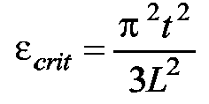
- the critical buckling strain ⁇ crit ⁇ 2 ⁇ t 2 3 ⁇ L 2 ( S.P.
- the grid being thicker than the membrane (usually more than twice as thick) the buckling - if occurring - is smoother and more regular than that of the thin electrolyte membrane (see Fig. 5-1 as an example) and the amplitude is lower.
- a metal grid is much tougher than a ceramic membrane. For large openings, a warping cannot be avoided, even with a grid of high aspect ratio. In this case a judicious design of grid will allow for a controlled warping.
- the grid geometry can be adapted to expected strains.
- the supporting grid exhibits 5 ⁇ m wide and 10 ⁇ m high grid lines (i.e. with the aspect ratio, height to width, of 2) and defining 20 to 200 ⁇ m wide grid openings (mesh size).
- a high aspect ratio ensures keeping a large efficiency of the cell, which is proportional to the active area exposed to the fuel gas flow divided by total area (can be called "filling factor").
- Membrane thickness and diameter of grid openings can be matched to obtain locally flat membranes within the grid openings, and relax thermal stresses to form a global deformation of the grid/membrane structure.
- Engineering to obtain predefined buckling may yield the requirement that the optimal grid geometry at the border of the membrane might be different from that in the center of the membrane. This is anyhow true for designs inspired by spin webs.
- the border elements could be filled with triangles to reinforce stiffness at the border (as in Fig. 5-1).
- the metallic grid plays at the same time the role of current collector. Being at the anode side, a porous Ni-electrolyte composite is deposited on top of the membrane on the grid side.
- the metallic grid guarantees the global connectivity of the porous layer, and allows reduction of the electrical conductivity of the porous electrode material.
- Preferential material for the grid is material that is well grown by electrochemical deposition, and in addition compatible with the anode-side function, such as nickel, palladium, copper, molybdenum, cobalt, ruthenium, iridium.
- Suitable seed layer materials are: Pt, Ir, Ru, etc., possibly also nickel or copper.
- the sub-layer or seed layer used for the electro-deposition of the metallic grid can be extended to provide a fine distribution of current. Only parts of this seed layer are then covered by the resist forming the mould for electro-deposition.
- This fine distribution may be a regular sub-grid structure. Its mesh size may be decreased to reach a high density of fme distribution lines, thus approaching an artificial porous structure.
- the fme distribution lines could be as thin as a few 100nm's. They could be organized as fractal structure carrying the current form the inside of the grid opening to the grid lines, having in the center a higher density of very narrow lines, and towards the grid line, a lower density of wider lines.
- the metallic grid may exhibit a polygonal pattern including in particular regular polygons such as triangles, squares, hexagons and octagons or irregular shapes including spider web type shapes and fractal structures.
- the invention also concerns an array of structures as described, which are fabricated on a common substrate and connected electrically to form an array of solid oxide fuel cells.
- Table 1 List of reference numbers.
- N° Description 1 Substrate 2 Current collector cathode 2a Additional grid lines of cathode 2b Electrical contact of cathode 3 Photoresist Mask 1 4 Electrolyte 5 Photoresist Mask 2 6 Photoresist Mask 3 7 Sub- Seed-layer/current collector anode 7a Intermediate sub- seed-layer 8 Photoresist Mask 4 mould 9 Grid/Electrical contact anode 9a Metallic grid 9b Electrical contact of the metallic grid 10 Porous anode 11 Photoresist Mask 5 12 Porous cathode
- the invention is a Positive electrode-Electrolyte-Negative electrode (PEN) structure of a solid oxide fuel cell including an anode grid 9 supporting an electrolyte membrane 4.
- the invention is used for mid-temperature to medium temperature range solid oxide fuel cells (300°C-600°C).
- the originality of the invention is the grid 9 serving as mechanical support of the thin electrolyte layer 4, as part of anode and as link for the electrical connections. This design allows placing the two electrical contacts (anode and cathode) on the same side of the support and facilitates the current collection.
- the supporting grid prevents thermal cracks in the electrolyte membrane 4 and allows improving the reactive area of the cell.
- the anode and cathode triple phase boundary lines (TPL) can also be improved by the inclusion of micro structured current collector meshes on the both sides of the electrolyte.
- TPL triple phase boundary lines
- the invention is related to a PEN structure for fuel cell applications comprising:
- the substrate 1 is a silicon, glass, Foturan TM , Pyrex TM or quartz flat wafer with diameter of for example 10 mm to 300 mm (Fig. 2-1).
- the electrolyte 4 is directly deposited onto the substrate 1 (possibly using a buffer layer) (Fig. 1-1).
- a metal mesh for cathode current collector 2 is deposited and patterned first (Figs. 1.1, Fig. 2-1, 2-2, 2-3). It is deposited by PVD, CVD, evaporation or PLD (pulsed laser deposition) and structured using photolithography and dry or wet etch.
- the collector 2 has the form of a two-dimensional mesh.
- the collector material is a conductive metal or oxide.
- the thickness t1 of the collector 2 is between 50nm and 200nm, its line width between 1mm and 10 ⁇ m and the spaces between lines between 5 ⁇ m and 500 ⁇ m.
- the electrolyte 4 is deposited by thin film technology (magnetron sputtering, pulsed laser deposition, chemical vapour deposition, spray pyrolysis, sol gel method, evaporation, screen printing, tape casting) and has a thickness between 50nm and 10 ⁇ m (Fig. 2-4).
- the electrolyte 4 is an oxygen ion conductor, typically ZrO 2 :Y 2 O 3 (YSZ) or Ce x Gd 1-x O 2-y (CGO), or other doped or undoped oxide ion conductors that usually exhibit the crystal structure of fluorites (for example: ZrO 2 , CeO 2 ,), corundum (for example: Y 2 O 3 ), perovskite (for example: La 1-x Sr x Ga 1-y Mg y O 3 ), tungsten bronzes (for example: SrBaNbO 6 ), pyrochlores or Aurivilius phases (for example:Bi 4 Ti 3 O 12 ).
- the electrolyte film is removed at the border where the contact to the cathode 2b is foreseen (Figs 2-5 and 2-6, dimension L2 ).
- the electrolyte membrane 4 is supported by grid 9 (Figs 2-10 to 2-12).
- a photoresist 6 is deposited and patterned first (Fig. 2-7) to allow for deposition of a seed layer 7, which is patterned by dissolving the resist (lift-off technique) arriving at the schematic structure of Fig. 2-9.
- the seed layer 7 is an electrical conductive metal such Cr, Au, Al, Cu, Pt, Pd, Ni, Mo, Ag, Ce, Gd or combination thereof. It is deposited preferentially by means of evaporation or magnetron sputtering.
- the mould 8 is prepared in the form of a patterned resist.
- the grid structure 9 is grown inside the mould by electrochemical deposition, the current being supplied through the seed layer 7 (Fig.
- the deposition can be performed by electroless plating.
- the growth of layer 9 yields the grid structure 9a, the anode contact 9b, which is of the same body as the grid.
- the material of the grid 9 is selected among electronically conductive metals (including Ni, Cu, Fe, Pt).
- the height t4 of the grid 9 is usually at minimum twice as thick as the electrolyte membrane 4 and between 1 ⁇ m and 100 ⁇ m, its line width w5 between 1 ⁇ m and 100 ⁇ m.
- the openings in the grid have dimensions w6 between 5 ⁇ m and 500 ⁇ m.
- the grid 9 mechanically supports the electrolyte membrane 4 and serves as current collector for the anode layer 10.
- the grid 9 covers the central part of the substrate to reach contacts for external electrical connections via contact 9b.
- the anode layer 10 is deposited by PVD, spray pyrolysis, CVD, PLD or evaporation over and in the spaces of the grid 9, covering the free surface of the electrolyte 4 (Fig. 2-13).
- the cathode contact on width L3 is protected by a sacrificial layer to avoid a short (by dry or wet etching or by lift-off).
- the thickness t5 of the anode layer 10 is between 50nm and 5 m.
- the material of the anode 10 is a porous composite of an electronic conductor (Ni, Pt, Ce, Gd%) and an ionic conductor (YSZ, CGO, ...), or a porous mixed conductor (LSCF, LSC).
- the liberation of the membrane 4 is preferentially carried out by deep dry etching process as available for silicon and silicon glass.
- An opening is formed into the substrate 1, of width w5 (Fig. 2-15), measuring 100 ⁇ m to 100mm.
- the cathode layer 12 is deposited by PVD, spray pyrolysis, CVD, PLD or evaporation over the electrolyte on the opposite side of the anode through the large opening in the substrate (dimension w5) of the support (Fig. 2-16).
- Cathode layer 12 covers the cathode current collector 2, to which there is automatically an electrical contact.
- the thickness t6 of the cathode is between 50nm and 5mm.
- the material of the cathode is a porous composite of an electronic conductive oxide (IrO 2 , RuO 2 ) and an ionic conductor (YSZ, CGO, LSC, LSCF%) or a porous mixed conductor such as (LaSr)(CoFe)O 3 (LSCF) or La 1-x Sr x CoO 3 (LSCO)
- Variations of the design shown in Figures 3-1 to 3-4 relate to the use of a seed layer 7 as current collector mesh on the anode side, and of a thin film structure as current collector on the cathode side.
- the grid structure 9 is grown on the entire seed layer 7. On both sides, no fine distribution of current is foreseen.
- a part of the seed layer 7 is used to distribute on a smaller scale the current within each opening of the grid 9. This fme distribution can be effectuated by a multitude of electrically connected lines 7a. The simplest case, with one additional sub-lattice is shown (as in Fig. 4). In Fig.
- an additional thin current collector 2 is introduced on the cathode side, one cathode mesh having the same pattern as and being below the structure 9 of the anode side, and the additional cathode grid 2a being spaced in between the anode grid 9.
- the two current collectors might be shifted with respect to each other (Fig. 4).
Abstract
A solid oxide fuel cell structure obtainable by selective electrochemical processing, comprising an electrolyte membrane (2) formed by a thin film more than 50nm but less than 10µm thick, covering a supporting structure (1) made of a bulk substrate, the supporting structure having at least one 100µm to 100mm wide opening that is covered by the electrolyte membrane (2). A metallic grid (9) is applied over the electrolyte membrane (2) and serves at the same time as structural element to support the membrane and as current collector. The metallic grid (9) has gridlines that are higher than the membrane thickness and whose height to width ratio is larger than 0.5, and a mesh size about 10 to 1000 times smaller than the width of said opening. The metallic grid (9) can be applied on top of a patterned metallic sub-layer structure (7,7a) arranged for supplying a fine distribution of current and increasing the density of electrolyte-electrode boundaries exposed to the fluid.
Description
- This invention relates to miniaturized solid oxide fuel cells requiring thin electrolyte membranes including electrodes and electrode contacts.
- The essential part of a solid oxide fuel cell (SOFC) consists of a ceramic plate made of an oxygen ionic conductor having the function of a solid electrolyte. The electrolyte plate is covered on the anode side by a porous metallic film, and on the cathode side by an electronic conductive oxide. Being exposed to a flow of air or oxygen (O2), this cathode layer takes up oxygen, and supplies the necessary electrons to form oxygen ions that traverse the electrolyte plate to reach the anode. There, a hydrocarbon gas mixture is oxidized by the oxygen ions and the electron charges are given to the anode electrode. The respective electrochemical potentials on the two sides are such that a voltage difference of roughly one Volt is installed allowing for recuperation of electrical power. The operation temperature of a classical SOFC amounts to 800 to 1000°C (see e.g. B.C.H. Steele, A. Heinzel, Materials for fuel-cell technologies, NATURE vol. 414, p. 345 (2001)). Operation procedures, application fields, and design depend crucially on the operation temperature. While high operation temperatures are good for large cells working continuously, high temperatures are unpractical for small cells and for automotive applications. In the first case, heat losses become too important, and in the second case, the time and energy consumption for start-up become too large. It is conceivable to operate SOFC's at temperatures as low as 500°C (R. Doshi, V.L. Richards, J.D. Carter, X. Wang, and M. Krumpelt, Development of SOFC's that operate at 500 °C, J.El.Chem.Soc. vol. 146, p.1273 (1999)). Such low temperatures are compatible with concepts of small SOFC cells in the centimeter dimension, able to be employed as energy source for portable electronic and electric devices. In such markets, miniaturized SOFC's are expected to have a large potential. Micro-SOFC's would be fuelled by liquid butane for instance.
- In miniaturized cells of lower temperature, the electrolyte plate or layer thickness must be reduced to reduce resistive losses inside the electrolyte. The ionic conductivity σ follows an exponential law of the form:

where A is a constant, Ea the activation energy, k the Boltzmann constant and T the absolute temperature. The internal resistance per unit area Ri of the cell can be written as:
- Ri is typically chosen as 0.1-0.2 Ωcm2 to allow for currents of 100 mA/cm2 without loss of output voltage. Taking as an example a Ce0.8Gd0.2O3 membrane, whose activation energy amounts to 0.7 eV, the thickness must be reduced by a factor 21 when decreasing the temperature from 1273K to 823K, provided that the conductivity of the material is the same for both thicknesses. This means that the electrolyte membrane cannot be anymore a self supported one of several 100µm to 1mm thickness, but must be thinned down to 5-50µm, and supported by another structure. Such supporting structure described in the literature is a 300 to 1200µm thick porous anode, consisting usually of a composite structure of nickel and yttrium stabilized zirconia (YSZ) (see, e.g. P. Holtapples, U. Vogt, and T. Graule, Ceramic materials for advanced solid oxide fuel cells, Adv. Eng.Mat. vol 292, p. 292 (2005)).
- An article Thin-film heterostructure solid oxide fuel cells by X Chen, N.J:Wu, L.Smith and A.Ignatiev, Applied Physics letters Vol. 84, Number 14, pages 2700-2702 describes a micro thin-film solid oxide fuel cell having a nickel foil substrate processed into a porous flat anode that has an array of circular pores.
- In US patent application
US 2005/0115889-A1 (pub. date June 2, 2005 ) entitled "Stressed thin film membrane islands", a stiffening structure is proposed to increase the stability of thin film membranes that are closing a large opening in a substrate. The proposed solutions include a grid structure superimposed to the thin film membrane to stiffen and support the membrane. The solution proposed is based on silicon micromachining techniques including deep silicon etching to define trenches. These are filled with nitride and oxide materials by means of thermal or plasma enhanced chemical vapor deposition. There are three major problems related to that invention: - 1) The membrane needs to be perforated to grow the supporting structure, risking leakage in case of SOFC application.
- 2) The supporting structure traverses the membrane, requiring insulating material for the supporting structure.
- 3) The supporting structure is produced in a rather complicated, delicate and costly way.
- The invention aims to remove some of these problems, and add additional functionality.
- In this invention, a different way is pursued. The membrane thinness is chosen to allow for compatibility with thin film and micromachining technology. An electrolyte membrane in the thickness range of 50nm to 10µm - deposited for example by sputtering or sol-gel techniques - closes a 100µm to 100 mm wide opening of a substrate of typically 0.5-1mm thickness. A metallic grid structure with a mesh size that is usually 10 to 1000 times smaller than the substrate opening supports the membrane to avoid cracking caused by excessive stresses and buckling. In addition, the metallic grid serves as current collector, preferentially on the anode side.
- This invention relates to miniaturized solid oxide fuel cells requiring thin electrolyte membranes including electrodes and electrode contacts. The thinness of the electrolyte membrane requires a supporting structure.
- The invention thus provides a solid oxide fuel cell structure obtainable by selective electrochemical processing, the structure comprising:
- an electrolyte membrane formed by a thin film more than 50nm but less than 10µm thick, covering a supporting structure made of a bulk substrate, the supporting structure having at least one opening that is 100µm to 100mm wide and that is covered by the electrolyte membrane; and
- a metallic grid applied over the electrolyte membrane and serving at the same time as structural element to support the membrane and as current collector, the metallic grid having gridlines that are higher than the membrane thickness and whose height to width ratio is larger than 0.5, preferably larger than 1 and even more preferably larger than 2.
- The metallic grid usually has a mesh size about 10 to 1000 times smaller than the width of said opening.
- By virtue of the grid's morphology and its aspect ratio, more space is left for the porous anode material which is easier to access. The new metallic grid is relatively thick and open, allowing better opportunities for 3-phase contact leading to better performance. It is also adapted to the expected thermal strains and stresses.
- Preferably, the metallic grid is applied on top of a patterned metallic sub-layer structure, the sub-layer structure comprising a wider pattern corresponding to the applied metallic grid, and a finer pattern that is not covered by the applied metallic grid, this finer pattern being arranged for supplying a fine distribution of current and increasing the density of electrolyte-electrode boundaries exposed to the fluid, and the metallic grid is on an anode side which in use is exposed to hydrocarbon fluid.
- Usually, the metallic grid is an anode current collector, and a cathode current collector structure is added on an opposite cathode side. The cathode current collector structure can have the same size and shape as the anode current collector grid, or the cathode current collector structure can have a different shape and/or be displaced with respect to the anode current collector grid.
- The invention removes some of the aforesaid problems with
US 2005/0115889-A1 , and adds additional functionality to the supporting structure: - 1) The membrane (electrolyte in our case) is not perforated during fabrication of the supporting structure.
- 2) The supporting structure is on one side only (anode) and can be made with a metallic material and with high aspect ratio.
- 3) The fabrication is less complicated and less expensive, as it uses electrochemical deposition of typically nickel. The mould for the creation of high aspect ratio grid structures is the not the silicon substrate on which the membrane is grown (as in
US 2005/0115889 ), instead we can use a patterned thick photoresist on top of the membrane to form the mold. - 4) The metal grid is used at the same time to work as current collector, thus supporting the functionality of thin porous electrodes, as typically used on the anode side.
- 5) A further extension introduces a thin metallic network structure on the side opposed to the supporting metallic grid to collect the current on this side and connect to a contact pad on the same side as the other one. The side with the contacts is preferentially the anode side, thus in reducing atmosphere, in order to avoid oxidation of contact metals.
- A critical issue is the stability of membranes at the operation temperature (500-600°C). Typically-used electrolyte materials such as CeGdO2 (CGO) or YSZ exhibit a large thermal expansion of around l2ppm/K, which in addition may depend on the oxygen partial pressure. The thermal expansion of Ni comes quite close (l3ppm/K). Hence the Ni grid and the electrolyte membrane expand by about the same amount when the temperature is raised. The substrate usually has much less expansion (Silicon: 3ppm/K, silicon glasses: 1 to 8ppm/K). Having a larger thermal expansion than the substrate, the membrane will buckle. The critical buckling strain

- The grid geometry can be adapted to expected strains. Typically the supporting grid exhibits 5µm wide and 10µm high grid lines (i.e. with the aspect ratio, height to width, of 2) and defining 20 to 200µm wide grid openings (mesh size). A high aspect ratio ensures keeping a large efficiency of the cell, which is proportional to the active area exposed to the fuel gas flow divided by total area (can be called "filling factor"). Membrane thickness and diameter of grid openings can be matched to obtain locally flat membranes within the grid openings, and relax thermal stresses to form a global deformation of the grid/membrane structure. Engineering to obtain predefined buckling may yield the requirement that the optimal grid geometry at the border of the membrane might be different from that in the center of the membrane. This is anyhow true for designs inspired by spin webs. In case of a hexagonal grid, the border elements could be filled with triangles to reinforce stiffness at the border (as in Fig. 5-1).
- The metallic grid plays at the same time the role of current collector. Being at the anode side, a porous Ni-electrolyte composite is deposited on top of the membrane on the grid side. The metallic grid guarantees the global connectivity of the porous layer, and allows reduction of the electrical conductivity of the porous electrode material. Preferential material for the grid is material that is well grown by electrochemical deposition, and in addition compatible with the anode-side function, such as nickel, palladium, copper, molybdenum, cobalt, ruthenium, iridium. Suitable seed layer materials are: Pt, Ir, Ru, etc., possibly also nickel or copper.
- Furthermore, the sub-layer or seed layer used for the electro-deposition of the metallic grid can be extended to provide a fine distribution of current. Only parts of this seed layer are then covered by the resist forming the mould for electro-deposition. This fine distribution may be a regular sub-grid structure. Its mesh size may be decreased to reach a high density of fme distribution lines, thus approaching an artificial porous structure. The fme distribution lines could be as thin as a few 100nm's. They could be organized as fractal structure carrying the current form the inside of the grid opening to the grid lines, having in the center a higher density of very narrow lines, and towards the grid line, a lower density of wider lines.
- The metallic grid may exhibit a polygonal pattern including in particular regular polygons such as triangles, squares, hexagons and octagons or irregular shapes including spider web type shapes and fractal structures.
- The invention also concerns an array of structures as described, which are fabricated on a common substrate and connected electrically to form an array of solid oxide fuel cells.
- The invention will be further described by way of example with reference to the accompanying drawings, in which:
- Fig. 1-1
- shows an embodiment of a fuel cell structure according to the invention, without a cathode collector grid;
- Fig. 1-2
- shows another embodiment of a fuel cell structure according to the invention with a cathode collector grid;
- Fig. 2
- illustrates in Figs. 2-1 to 2-16 the successive steps for the fabrication of the structure of Fig. 1-2;
- Fig. 3
- illustrates in Figs. 3-1 to 3-4 variations where the anode grid is grown on a sub-layer or seed layer;
- Fig. 4
- is a schematic top view showing the pattern of the metallic anode grid, sub-layer or seed layer and current collector; and
- Fig. 5
- shows in Figs. 5-1 and 5-2 photographs of examples of different grid shapes.
- For convenience, the reference numbers used in the drawings are shown in Table 1.
Table 1: List of reference numbers. N° Description 1 Substrate 2 Current collector cathode 2a Additional grid lines of cathode 2b Electrical contact of cathode 3 Photoresist Mask 14 Electrolyte 5 Photoresist Mask 26 Photoresist Mask 3 7 Sub- Seed-layer/ current collector anode 7a Intermediate sub- seed- layer 8 Photoresist Mask 4 mould9 Grid/ Electrical contact anode 9a Metallic grid 9b Electrical contact of the metallic grid 10 Porous anode 11 Photoresist Mask 512 Porous cathode - Fig. 1-1 is a schematic view of a PEN structure of a fuel cell composed of a
porous cathode 12, athin electrolyte film 4 and porous anode layers 10. The PEN is mounted on asubstrate 1 and mechanically supported by ametallic grid 9a which is also a part of the anode current collector.Electrical connections - Fig. 1-2 also shows a PEN structure of a fuel cell like that of Fig. 1-1 but additionally with a
current collector grid 2 on the cathode side. - Fig. 2 illustrates the process flow steps for the fabrication of the device shown in Fig. 1-2.
Steps 1 to 3 are skipped for the device shown in Fig. 1-1. The process steps of Figs. 2-1 to 2-16 are as follows: - Fig 2-1: Deposition of a
metallic layer 2 of thickness t1 by PVD on asubstrate 1 of thickness t0.Layer 2 will constitute the current collector on the cathode side and the electrical contact for the cathode. - Fig. 2-2: Deposition and structuration of a photo-sensible polymer layer 3 serving as first photoresist mask for the
current collector 2 etch. - Fig. 2-3: Dry etching of the
current collector 2 and removal of the photoresist mask 3.Layer 2 is now a mesh with line width w1 and line spacing w2. On the border of the membrane, anelectrical contact 2b of dimension L1 is also structured. - Fig. 2-4: Deposition of the
electrolyte layer 4 of thickness t2. - Fig. 2-5: Deposition and structuration of a photo-
sensible polymer layer 5 serving as second photoresist mask for theelectrolyte 4 etch. - Fig. 2-6: Dry etching of an opening ("via hole") of dimension L2 in the
electrolyte 4 and removal of thephotoresist mask 5. The "via hole" serves for making electrical contact with thecathode 2 via itscontact 2b. - Fig. 2-7: Deposition and structuration of a photo-
sensible polymer layer 6 serving as third photoresist mask for the lift-off of theseed layer 7. - Fig. 2-8: Deposition of a
metallic layer 7 of thickness t3 by PVD over thephotoresist mask 6.Layer 7 serves as seed layer for the electrodeposition and as current collector for the anode, depending on the design shown in Fig. 3. - Fig. 2-9: Removal of the
photoresist 6.Seed layer 7 is structured by lift-off with line width w3 and line spacing w4. A gap of dimension L3 is not covered bylayer 7. This gap serves as via for the electrical connection of thecathode 2. On one border, themembrane 4 is covered bylayer 7 over a dimension L4. Theseed layer 7 is connected to an electrical contact on the border of the substrate for electrodeposition. - Fig. 2-10: Deposition and structuration of a photo-
sensible polymer layer 8 serving as mould for the electrodeposited layer 9 (9a and 9b). - Fig. 2-11: Electrodeposition of the
metallic grid 9a andcontact 9b of thickness t4. Thegrid 9a has a line width w5 and a line spacing w6 (Fig. 2-12). The metallic grid 9 also serves aselectrical contact 9b for the anode covering a length L4 of theseed layer 7. - Fig. 2-12: Removal of the
photoresist mould 8. The thickness of the metallic grid is t4, the line width w5 and the space between lines w6. - Fig. 2-13: Deposition of the
porous anode layer 10 of thickness t5 with a hard mask protecting the electrical contact of the cathode. - Fig. 2-14: Deposition and structuration of a photo
sensible polymer layer 11 serving as fifth photoresist mask for thesubstrate 1 backside etch. - Fig. 2-15: Dry etching of an opening of size w5 in the
substrate 1. - Fig. 2-16: Deposition of a
porous cathode layer 12 of thickness t6 on the backside of thesubstrate 1. - Fig. 3-1 is a schematic cross-sectional view of a part of the metallic grid 9 supporting the
electrolyte 4,anode 10 andcathode 12. In this example, the whole sub-or seed-layer 7 is covered by the metallic grid 9. The current collector of thecathode 2 is placed under and only under each grid element. - Fig. 3-2 is like Fig. 3-1 where in addition some
parts 7a of the sub- or seed-layer 7 are not covered by the metallic grid 9 and serve as current collector for theanode 10. - Fig. 3-3 is like Fig. 3-1, where a current collector of the
cathode 2 is introduced that has its lines at the same position as the lines of thegrid 9a andadditional grid lines 2a in-between. - Fig. 3-4 represents a combination of Figs. 3-2 and 3-3.
Parts 7a of theseed layer 7 are not covered by the metallic grid 9 and serve as current collector for theanode 10, and someparts 2a of the current collector of thecathode 2 are not at the same position as the metallic grid 9. In this case, theextra lines 7a of theseed layer cathode 2 can overlay one another (as shown) or can intersect with one another. - Fig. 4 is a schematic top view of the metallic grid 9,
seed layer 7 and current collector of thecathode 2, showing the extra seed-layer lines 7a and the extracathode collector lines 2a. The line widths of the three networks are between 0µm and 50µm and not necessarily equal. The spaces between the lines of these three networks are between 1µm and 500µm and not necessarily equal. The centres of the cells of the different networks can be super-imposed or displaced by distances between 1µm and 100µm. - Fig. 5-1 is a photograph of an example of a nickel grid of triangular shape on top of afree-standing CGO membrane. Side length of triangles: 50 µm. In this case, the triangular shapes are arranged to form a series of hexagons.
- Fig. 5-2 is a photograph of an example of a nickel grid of hexagonal shape on top of a free-standing CGO membrane. Side length of hexagons: 50 µm. In this photo, the controlled buckling of the membrane in the grid is clearly visible.
- The invention is a Positive electrode-Electrolyte-Negative electrode (PEN) structure of a solid oxide fuel cell including an anode grid 9 supporting an
electrolyte membrane 4. The invention is used for mid-temperature to medium temperature range solid oxide fuel cells (300°C-600°C). The originality of the invention is the grid 9 serving as mechanical support of thethin electrolyte layer 4, as part of anode and as link for the electrical connections. This design allows placing the two electrical contacts (anode and cathode) on the same side of the support and facilitates the current collection. The supporting grid prevents thermal cracks in theelectrolyte membrane 4 and allows improving the reactive area of the cell. The anode and cathode triple phase boundary lines (TPL) can also be improved by the inclusion of micro structured current collector meshes on the both sides of the electrolyte. The original and easy micro fabrication process of this structure is also part of the present invention. - The invention is related to a PEN structure for fuel cell applications comprising:
- a
substrate 1 with a "large" opening of width w5 from 100µm to 100mm; - an
electrolyte membrane 4 closing the said opening; - a metallic grid 9 supporting the
membrane 4 and being part of the anode; - an
anode 10; - a
cathode 12; - a current collector mesh formed by the grid 9 on the anode side;
- a
current collector mesh 2 on the cathode side; - an
electrical contact 9b to the anode, located on the anode side; and - an
electrical contact 2b to the cathode, also located on the anode side. - The
substrate 1 is a silicon, glass, Foturan™, Pyrex™ or quartz flat wafer with diameter of for example 10 mm to 300 mm (Fig. 2-1). - In a first design, the
electrolyte 4 is directly deposited onto the substrate 1 (possibly using a buffer layer) (Fig. 1-1). In a second design, a metal mesh for cathodecurrent collector 2 is deposited and patterned first (Figs. 1.1, Fig. 2-1, 2-2, 2-3). It is deposited by PVD, CVD, evaporation or PLD (pulsed laser deposition) and structured using photolithography and dry or wet etch. Thecollector 2 has the form of a two-dimensional mesh. The collector material is a conductive metal or oxide. The thickness t1 of thecollector 2 is between 50nm and 200nm, its line width between 1mm and 10µm and the spaces between lines between 5µm and 500µm. - The
electrolyte 4 is deposited by thin film technology (magnetron sputtering, pulsed laser deposition, chemical vapour deposition, spray pyrolysis, sol gel method, evaporation, screen printing, tape casting) and has a thickness between 50nm and 10µm (Fig. 2-4). Theelectrolyte 4 is an oxygen ion conductor, typically ZrO2:Y2O3 (YSZ) or CexGd1-xO2-y (CGO), or other doped or undoped oxide ion conductors that usually exhibit the crystal structure of fluorites (for example: ZrO2, CeO2,), corundum (for exemple: Y2O3), perovskite (for example: La1-xSrxGa1-yMgyO3), tungsten bronzes (for example: SrBaNbO6), pyrochlores or Aurivilius phases (for example:Bi4Ti3O12). The electrolyte film is removed at the border where the contact to thecathode 2b is foreseen (Figs 2-5 and 2-6, dimension L2). - The
electrolyte membrane 4 is supported by grid 9 (Figs 2-10 to 2-12). For its fabrication, aphotoresist 6 is deposited and patterned first (Fig. 2-7) to allow for deposition of aseed layer 7, which is patterned by dissolving the resist (lift-off technique) arriving at the schematic structure of Fig. 2-9. Theseed layer 7 is an electrical conductive metal such Cr, Au, Al, Cu, Pt, Pd, Ni, Mo, Ag, Ce, Gd or combination thereof. It is deposited preferentially by means of evaporation or magnetron sputtering. In the next step themould 8 is prepared in the form of a patterned resist. The grid structure 9 is grown inside the mould by electrochemical deposition, the current being supplied through the seed layer 7 (Fig. 2-11), which is connected on the wafer level to a power supply. Alternatively, the deposition can be performed by electroless plating. The growth of layer 9 yields thegrid structure 9a, theanode contact 9b, which is of the same body as the grid. The material of the grid 9 is selected among electronically conductive metals (including Ni, Cu, Fe, Pt). The height t4 of the grid 9 is usually at minimum twice as thick as theelectrolyte membrane 4 and between 1µm and 100µm, its line width w5 between 1µm and 100µm. The openings in the grid have dimensions w6 between 5µm and 500µm. - The grid 9 mechanically supports the
electrolyte membrane 4 and serves as current collector for theanode layer 10. The grid 9 covers the central part of the substrate to reach contacts for external electrical connections viacontact 9b. Theanode layer 10 is deposited by PVD, spray pyrolysis, CVD, PLD or evaporation over and in the spaces of the grid 9, covering the free surface of the electrolyte 4 (Fig. 2-13). The cathode contact on width L3 is protected by a sacrificial layer to avoid a short (by dry or wet etching or by lift-off). The thickness t5 of theanode layer 10 is between 50nm and 5 m. The material of theanode 10 is a porous composite of an electronic conductor (Ni, Pt, Ce, Gd...) and an ionic conductor (YSZ, CGO, ...), or a porous mixed conductor (LSCF, LSC...). - The liberation of the
membrane 4 is preferentially carried out by deep dry etching process as available for silicon and silicon glass. First a thick resist 11 is deposited, and patterned by photolithography (Fig 2-14). The resist serves as mask for deep dry etching. An opening is formed into thesubstrate 1, of width w5 (Fig. 2-15), measuring 100µm to 100mm. - The
cathode layer 12 is deposited by PVD, spray pyrolysis, CVD, PLD or evaporation over the electrolyte on the opposite side of the anode through the large opening in the substrate (dimension w5) of the support (Fig. 2-16).Cathode layer 12 covers the cathodecurrent collector 2, to which there is automatically an electrical contact. The thickness t6 of the cathode is between 50nm and 5mm. The material of the cathode is a porous composite of an electronic conductive oxide (IrO2, RuO2) and an ionic conductor (YSZ, CGO, LSC, LSCF...) or a porous mixed conductor such as (LaSr)(CoFe)O3 (LSCF) or La1-xSrxCoO3 (LSCO) - Variations of the design shown in Figures 3-1 to 3-4 relate to the use of a
seed layer 7 as current collector mesh on the anode side, and of a thin film structure as current collector on the cathode side. In Figure 3-1, the grid structure 9 is grown on theentire seed layer 7. On both sides, no fine distribution of current is foreseen. In Fig. 3-2, a part of theseed layer 7 is used to distribute on a smaller scale the current within each opening of the grid 9. This fme distribution can be effectuated by a multitude of electrically connectedlines 7a. The simplest case, with one additional sub-lattice is shown (as in Fig. 4). In Fig. 3-3, an additional thincurrent collector 2 is introduced on the cathode side, one cathode mesh having the same pattern as and being below the structure 9 of the anode side, and theadditional cathode grid 2a being spaced in between the anode grid 9. As a further variation, the two current collectors might be shifted with respect to each other (Fig. 4).
Claims (17)
- Solid oxide fuel cell structure obtainable by selective electrochemical processing, the structure comprising:- an electrolyte membrane formed by a thin film more than 50nm but less than 10 µm thick, covering a supporting structure made of a bulk substrate, the supporting structure having at least one opening that is 100µm to 100mm wide and that is covered by the electrolyte membrane; and- a metallic grid applied over the electrolyte membrane and serving at the same time as structural element to support the membrane and as current collector, the metallic grid having gridlines that are higher than the membrane thickness and whose height to width ratio is larger than 0.5.
- Structure of claim 1, wherein the metallic grid has a mesh size about 10 to 1000 times smaller than the width of said opening.
- Structure of claim 1 or 2, wherein:- the metallic grid is applied on top of a patterned metallic sub-layer structure,- the sub-layer structure comprises a wider pattern corresponding to the applied metallic grid, and a finer pattern that is not covered by the applied metallic grid, said finer pattern being arranged for supplying a fine distribution of current and increasing the density of electrolyte-electrode boundaries exposed to the fluid, and- the metallic grid is on an anode side which in use is exposed to hydrocarbon fluid.
- Structure of claim 1, 2 or 3, wherein the metallic grid is an anode current collector, and a current collector structure is added on an opposite cathode side.
- Structure of claim 4, wherein the cathode current collector structure has the same size and shape as the anode current collector grid.
- Structure of claim 4 or 5, wherein the cathode current collector structure has a different shape and/or is displaced with respect to the anode current collector grid.
- Structure of claim 4, 5 or 6, comprising a first electrical contact to the metallic anode grid, the first contact being located on an anode side of the structure, and a second electrical contact to the cathode, the second contact also being located on the anode side of the structure
- Structure of any preceding claim, wherein the electrolyte thin film is selected from CeO2:Gd2O3 (CGO), ZrO2:Y2O3 (YSZ), and doped or undoped oxide ion conductors that exhibit the crystal structure of fluorites, corundum, perovskite, tungsten bronzes, pyrochlores or Aurivilius phases.
- Structure of any preceding claim, wherein the metallic grid is made from at least one metal selected from Ni, Cu, Pt, Cr, Mo, Ag, Co, and Pd.
- Structure of any preceding claim, further comprising a porous anode film in particular selected from NiOx and Ni-(electrolyte) composite.
- Structure of any preceding claim, further comprising a porous cathode film in particular selected from a porous mixed conductor such as (LaSr)(CoFe)O3 (LSCF) or La1-xSrxCoO3 (LSCO); and composites of an electronically conductive oxide and an ionically conductive oxide.
- Structure of any preceding claim, wherein the grid exhibits a polygonal pattern including in particular regular polygons such as triangles, squares, hexagons and octagons.
- Structure of any one of claims 1 to 11, wherein the grid exhibits irregular shapes including spider web type shapes and fractal structures.
- An array of structures of any preceding claim, which are fabricated on a common substrate and connected electrically to form an array of solid oxide fuel cells.
- A method of producing the structure of any preceding claim by photolithographic patterning and electrochemical, physical and chemical vapour processing of successive layers on an etchable substrate, wherein the membrane and the metallic grid are applied to the substrate, and the substrate is etched to provide said opening.
- The method of claim 15, wherein the substrate opening is etched by dry etching in SF6 gas or by wet etching in alkaline solutions.
- The method of claim 15 or 16, wherein the metallic grid is moulded in a polymer mould, in particular of photoresist.
Priority Applications (4)
| Application Number | Priority Date | Filing Date | Title |
|---|---|---|---|
| EP05112175A EP1798800A1 (en) | 2005-12-14 | 2005-12-14 | Metallic supporting grid for ultrathin electrolyte membranes in solid oxide fuel cells |
| US12/097,113 US20080311434A1 (en) | 2005-12-14 | 2006-12-13 | Metallic Supporting Grid for Thin Electrolyte Membrane in Solid Oxide Fuel Cells |
| PCT/EP2006/069688 WO2007068726A1 (en) | 2005-12-14 | 2006-12-13 | Metallic supporting grid for ultrathin electrolyte membranes in solid oxide fuel cells |
| EP06841355A EP1972025A1 (en) | 2005-12-14 | 2006-12-13 | Metallic supporting grid for ultrathin electrolyte membranes in solid oxide fuel cells |
Applications Claiming Priority (1)
| Application Number | Priority Date | Filing Date | Title |
|---|---|---|---|
| EP05112175A EP1798800A1 (en) | 2005-12-14 | 2005-12-14 | Metallic supporting grid for ultrathin electrolyte membranes in solid oxide fuel cells |
Publications (1)
| Publication Number | Publication Date |
|---|---|
| EP1798800A1 true EP1798800A1 (en) | 2007-06-20 |
Family
ID=37547523
Family Applications (2)
| Application Number | Title | Priority Date | Filing Date |
|---|---|---|---|
| EP05112175A Withdrawn EP1798800A1 (en) | 2005-12-14 | 2005-12-14 | Metallic supporting grid for ultrathin electrolyte membranes in solid oxide fuel cells |
| EP06841355A Withdrawn EP1972025A1 (en) | 2005-12-14 | 2006-12-13 | Metallic supporting grid for ultrathin electrolyte membranes in solid oxide fuel cells |
Family Applications After (1)
| Application Number | Title | Priority Date | Filing Date |
|---|---|---|---|
| EP06841355A Withdrawn EP1972025A1 (en) | 2005-12-14 | 2006-12-13 | Metallic supporting grid for ultrathin electrolyte membranes in solid oxide fuel cells |
Country Status (3)
| Country | Link |
|---|---|
| US (1) | US20080311434A1 (en) |
| EP (2) | EP1798800A1 (en) |
| WO (1) | WO2007068726A1 (en) |
Cited By (1)
| Publication number | Priority date | Publication date | Assignee | Title |
|---|---|---|---|---|
| EP3866239A4 (en) * | 2018-10-12 | 2023-02-01 | Hitachi High-Tech Corporation | Fuel battery cell |
Families Citing this family (8)
| Publication number | Priority date | Publication date | Assignee | Title |
|---|---|---|---|---|
| US20130256122A1 (en) * | 2010-08-31 | 2013-10-03 | President And Fellows Of Harvard College | Electrochemically functional membranes |
| KR101175236B1 (en) | 2011-01-25 | 2012-08-23 | 한국에너지기술연구원 | Unit cell of SOFC fuel-cell |
| EP2559996B1 (en) * | 2011-08-16 | 2017-11-22 | Nxp B.V. | Gas sensor |
| US8790850B2 (en) * | 2012-03-01 | 2014-07-29 | Institute Of Nuclear Energy Research | Current collection apparatus and method of processing for a solid oxide fuel cell thereof |
| KR102027117B1 (en) * | 2012-06-08 | 2019-10-01 | 주식회사 미코 | Current collector for fuel cell and stack structure including the same |
| US20150099061A1 (en) * | 2013-10-08 | 2015-04-09 | Phillips 66 Company | Formation of solid oxide fuel cells |
| US9453807B2 (en) | 2014-04-08 | 2016-09-27 | Ams International Ag | Thermal conductivity gas sensor with amplification material |
| KR102492733B1 (en) | 2017-09-29 | 2023-01-27 | 삼성디스플레이 주식회사 | Copper plasma etching method and manufacturing method of display panel |
Citations (4)
| Publication number | Priority date | Publication date | Assignee | Title |
|---|---|---|---|---|
| US20030012994A1 (en) * | 2000-11-27 | 2003-01-16 | Keiko Kushibiki | Single cell for fuel cell and solid oxide fuel cell |
| EP1284520A2 (en) * | 2001-08-13 | 2003-02-19 | Nissan Motor Co., Ltd. | Cell plate structure for solid electrolyte fuel cell, solid electrolyte fuel cell and related manufacturing method |
| US20040121222A1 (en) * | 2002-09-10 | 2004-06-24 | Partho Sarkar | Crack-resistant anode-supported fuel cell |
| WO2005030376A1 (en) * | 2003-09-23 | 2005-04-07 | Lilliputian Systems, Inc. | Stressed thin-film membrane islands |
Family Cites Families (3)
| Publication number | Priority date | Publication date | Assignee | Title |
|---|---|---|---|---|
| US6638654B2 (en) * | 1999-02-01 | 2003-10-28 | The Regents Of The University Of California | MEMS-based thin-film fuel cells |
| US6960403B2 (en) * | 2002-09-30 | 2005-11-01 | The Regents Of The University Of California | Bonded polyimide fuel cell package and method thereof |
| JP5031187B2 (en) * | 2004-11-19 | 2012-09-19 | 東邦瓦斯株式会社 | SOLAR ELECTRODE FOR SOLID OXIDE FUEL CELL AND SOLID OXIDE FUEL CELL |
-
2005
- 2005-12-14 EP EP05112175A patent/EP1798800A1/en not_active Withdrawn
-
2006
- 2006-12-13 US US12/097,113 patent/US20080311434A1/en not_active Abandoned
- 2006-12-13 EP EP06841355A patent/EP1972025A1/en not_active Withdrawn
- 2006-12-13 WO PCT/EP2006/069688 patent/WO2007068726A1/en active Application Filing
Patent Citations (4)
| Publication number | Priority date | Publication date | Assignee | Title |
|---|---|---|---|---|
| US20030012994A1 (en) * | 2000-11-27 | 2003-01-16 | Keiko Kushibiki | Single cell for fuel cell and solid oxide fuel cell |
| EP1284520A2 (en) * | 2001-08-13 | 2003-02-19 | Nissan Motor Co., Ltd. | Cell plate structure for solid electrolyte fuel cell, solid electrolyte fuel cell and related manufacturing method |
| US20040121222A1 (en) * | 2002-09-10 | 2004-06-24 | Partho Sarkar | Crack-resistant anode-supported fuel cell |
| WO2005030376A1 (en) * | 2003-09-23 | 2005-04-07 | Lilliputian Systems, Inc. | Stressed thin-film membrane islands |
Non-Patent Citations (2)
| Title |
|---|
| JANKOWSKI A F ET AL: "TESTING OF SOLID-OXIDE FUEL CELLS FOR MICRO TO MACRO POWER GENERATION", PROCEEDINGS OF THE INTERNATIONAL SYMPOSIUM ON SOLID OXIDE FUEL CELLS, XX, XX, vol. 99, no. 19, 17 October 1999 (1999-10-17), pages 932 - 937, XP009069051 * |
| SRIKAR V T ET AL: "Structural design considerations for micromachined solid-oxide fuel cells", JOURNAL OF POWER SOURCES, ELSEVIER, AMSTERDAM, NL, vol. 125, no. 1, 2 January 2004 (2004-01-02), pages 62 - 69, XP004480787, ISSN: 0378-7753 * |
Cited By (1)
| Publication number | Priority date | Publication date | Assignee | Title |
|---|---|---|---|---|
| EP3866239A4 (en) * | 2018-10-12 | 2023-02-01 | Hitachi High-Tech Corporation | Fuel battery cell |
Also Published As
| Publication number | Publication date |
|---|---|
| US20080311434A1 (en) | 2008-12-18 |
| WO2007068726A1 (en) | 2007-06-21 |
| EP1972025A1 (en) | 2008-09-24 |
Similar Documents
| Publication | Publication Date | Title |
|---|---|---|
| EP1798800A1 (en) | Metallic supporting grid for ultrathin electrolyte membranes in solid oxide fuel cells | |
| JP3731648B2 (en) | Single cell for fuel cell and solid oxide fuel cell | |
| US6645656B1 (en) | Thin film solid oxide fuel cell and method for forming | |
| Evans et al. | Review on microfabricated micro-solid oxide fuel cell membranes | |
| Radhakrishnan et al. | Estimation of Charge-Transfer Resistivity of La0. 8Sr0. 2MnO3 Cathode on Y 0.16 Zr0. 84 O 2 Electrolyte Using Patterned Electrodes | |
| US7510819B2 (en) | Thin film solid oxide fuel cell with lithographically patterned electrolyte and anode layers | |
| Chen et al. | Thin-film heterostructure solid oxide fuel cells | |
| US6969664B2 (en) | Micro silicon fuel cell, method of fabrication and self-powered semiconductor device integrating a micro fuel cell | |
| Johnson et al. | An experimental investigation into micro-fabricated solid oxide fuel cells with ultra-thin La0. 6Sr0. 4Co0. 8Fe0. 2O3 cathodes and yttria-doped zirconia electrolyte films | |
| US6926852B2 (en) | Cell plate structure for solid electrolyte fuel cell, solid electrolyte fuel cell and related manufacturing method | |
| Su et al. | Nanoscale membrane electrolyte array for solid oxide fuel cells | |
| Park et al. | Fabrication of the large area thin-film solid oxide fuel cells | |
| US7381492B2 (en) | Thin film solid oxide fuel cell and method for forming | |
| KR101002044B1 (en) | Micro fuel cell and the fabrication method thereof, and micro fuel cell stack using the same | |
| KR20080085092A (en) | Membrane electrode assembly in solid oxide fuel cells | |
| CN1591949B (en) | Current collector supported fuel cell | |
| JP2003323901A (en) | Fuel cell body and its manufacturing method | |
| EP1672728A1 (en) | High performance fuel cell electrode and method for manufacturing same | |
| Johnson et al. | Fabrication and electrochemical performance of thin-film solid oxide fuel cells with large area nanostructured membranes | |
| Buyukaksoy et al. | Optimization of redox stable Ni-YSZ anodes for SOFCs by two-step infiltration | |
| KR20100104153A (en) | Anode-supported solid oxide fuel cell having pore-gradient structure for forming thin film electrolyte and the fabrication method thereof | |
| Su et al. | Cup-shaped yttria-doped barium zirconate membrane fuel cell array | |
| WO2011016865A2 (en) | Solid oxide electrolytic device | |
| US20030235753A1 (en) | Method for fabricating high surface area catalysts | |
| Jin et al. | Suppressed Carbon Deposition Behavior in Nickel/Yittria-Stablized Zirconia Anode with SrZr0. 95Y0. 05O3− α in Dry Methane Fuel |
Legal Events
| Date | Code | Title | Description |
|---|---|---|---|
| PUAI | Public reference made under article 153(3) epc to a published international application that has entered the european phase |
Free format text: ORIGINAL CODE: 0009012 |
|
| AK | Designated contracting states |
Kind code of ref document: A1 Designated state(s): AT BE BG CH CY CZ DE DK EE ES FI FR GB GR HU IE IS IT LI LT LU LV MC NL PL PT RO SE SI SK TR |
|
| AX | Request for extension of the european patent |
Extension state: AL BA HR MK YU |
|
| AKX | Designation fees paid | ||
| REG | Reference to a national code |
Ref country code: DE Ref legal event code: 8566 |
|
| STAA | Information on the status of an ep patent application or granted ep patent |
Free format text: STATUS: THE APPLICATION IS DEEMED TO BE WITHDRAWN |
|
| 18D | Application deemed to be withdrawn |
Effective date: 20071221 |