EP1282071A2 - Power-on reset circuit for an IC card - Google Patents
Power-on reset circuit for an IC card Download PDFInfo
- Publication number
- EP1282071A2 EP1282071A2 EP02255330A EP02255330A EP1282071A2 EP 1282071 A2 EP1282071 A2 EP 1282071A2 EP 02255330 A EP02255330 A EP 02255330A EP 02255330 A EP02255330 A EP 02255330A EP 1282071 A2 EP1282071 A2 EP 1282071A2
- Authority
- EP
- European Patent Office
- Prior art keywords
- circuit
- reset
- voltage
- power
- reset signal
- Prior art date
- Legal status (The legal status is an assumption and is not a legal conclusion. Google has not performed a legal analysis and makes no representation as to the accuracy of the status listed.)
- Granted
Links
Images



Classifications
-
- G—PHYSICS
- G06—COMPUTING OR CALCULATING; COUNTING
- G06K—GRAPHICAL DATA READING; PRESENTATION OF DATA; RECORD CARRIERS; HANDLING RECORD CARRIERS
- G06K19/00—Record carriers for use with machines and with at least a part designed to carry digital markings
- G06K19/06—Record carriers for use with machines and with at least a part designed to carry digital markings characterised by the kind of the digital marking, e.g. shape, nature, code
- G06K19/067—Record carriers with conductive marks, printed circuits or semiconductor circuit elements, e.g. credit or identity cards also with resonating or responding marks without active components
- G06K19/07—Record carriers with conductive marks, printed circuits or semiconductor circuit elements, e.g. credit or identity cards also with resonating or responding marks without active components with integrated circuit chips
- G06K19/0701—Record carriers with conductive marks, printed circuits or semiconductor circuit elements, e.g. credit or identity cards also with resonating or responding marks without active components with integrated circuit chips at least one of the integrated circuit chips comprising an arrangement for power management
-
- G—PHYSICS
- G06—COMPUTING OR CALCULATING; COUNTING
- G06F—ELECTRIC DIGITAL DATA PROCESSING
- G06F1/00—Details not covered by groups G06F3/00 - G06F13/00 and G06F21/00
- G06F1/24—Resetting means
-
- G—PHYSICS
- G06—COMPUTING OR CALCULATING; COUNTING
- G06K—GRAPHICAL DATA READING; PRESENTATION OF DATA; RECORD CARRIERS; HANDLING RECORD CARRIERS
- G06K19/00—Record carriers for use with machines and with at least a part designed to carry digital markings
- G06K19/06—Record carriers for use with machines and with at least a part designed to carry digital markings characterised by the kind of the digital marking, e.g. shape, nature, code
- G06K19/067—Record carriers with conductive marks, printed circuits or semiconductor circuit elements, e.g. credit or identity cards also with resonating or responding marks without active components
- G06K19/07—Record carriers with conductive marks, printed circuits or semiconductor circuit elements, e.g. credit or identity cards also with resonating or responding marks without active components with integrated circuit chips
- G06K19/0723—Record carriers with conductive marks, printed circuits or semiconductor circuit elements, e.g. credit or identity cards also with resonating or responding marks without active components with integrated circuit chips the record carrier comprising an arrangement for non-contact communication, e.g. wireless communication circuits on transponder cards, non-contact smart cards or RFIDs
-
- H—ELECTRICITY
- H03—ELECTRONIC CIRCUITRY
- H03K—PULSE TECHNIQUE
- H03K17/00—Electronic switching or gating, i.e. not by contact-making and –breaking
- H03K17/22—Modifications for ensuring a predetermined initial state when the supply voltage has been applied
Definitions
- the present invention relates to power-on reset circuit which is utilized for an IC card that obtains electric power from the external electric power supply source without contacting, for example, through electromagnetic waves.
- an IC card with a semiconductor integrated circuit device is becoming widespread.
- the IC card has a capability of exchanging information between an external reader/writer apparatus and a semiconductor integrated circuit device mounted in the IC card. This makes it possible to store necessary information in an internal nonvolatile memory of the semiconductor integrated circuit device, and conversely, to read information from the nonvolatile memory.
- By utilizing such an IC card it is possible to realize a variety of functions that a magnetic card has carried out conventionally.
- the IC card With a recent advance in the technology for large packing densities, the IC card has included a nonvolatile memory with a larger capacity. Accordingly, a multi-purpose card having a plurality of applications included in one IC card is also becoming widespread.
- non-contact type IC card system for the IC card has been studied in which the supply of electric power without contacting as well as data communication are carried out, utilizing electromagnetic waves with carrier frequencies of the order of several MHz to several tens of MHz.
- the IC card has advantages such as decrease in maintenance cost and easy handling.
- non-contact type IC card serving as a ticket for taking transport facilities such as a train and a bus allows a person to go through the ticket gate only by ways of holding the non-contact type IC card over the ticket gate (hereinafter referred to as "holding process"), or making the non-contact type IC card touch to the ticket gate in a moment (hereinafter referred to as "touch-and-go process").
- IC card in such a non-contact type IC card system, considered are various manners for information exchange between an IC card and a reader/writer apparatus. Some examples are given as follows: (1) a way of holding the IC card over the reader/writer apparatus at a small distance within approximately several cm (holding process); (2) a way of inserting the IC card to a card holder set in the reader/writer apparatus (inserting process); and (3) a way of supplying voltage to the IC card at power-on in setting the IC card to the reader/writer apparatus.
- Japanese Laid-Open Patent Publication No. 269327/1998 discloses a circuit configuration for carrying out the power-on reset with respect to the non-contact type IC card.
- the power of the logic circuit is shut off on the reset operation by detection of power supply voltage in an analog mode. This shut-off does not apply voltage to an input/output circuit to/from a microcomputer and a microcomputer circuit.
- the configuration will be described more specifically below.
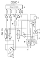
- FIG. 10 is a circuit diagram of an example of the circuit configuration. Voltage outputted from an antenna coil 51 is supplied to each circuits after supplied to REG-A 55 and REG-B 56 as regulator circuits, and VREF 57 as a reference voltage producing circuit. From the REG-A 55, voltage is supplied to a microcomputer 64 and an interface section thereof. Further, from the REG-B 56, voltage is supplied to a CLK reproducing circuit 53, a reset producing circuit 54, an MOD 66 as a modulation circuit, a DEMO 67 as a demodulation circuit, and (+) terminal of a comparator circuit 59.
- the output from the VREF 57 as a reference voltage producing circuit is for the voltage supply to the REG-A 55 and the REG-B 56, and a switch 60 is provided on the path to the REG-A 55 to control a power rising sequence. Further, the output from the VREF 57 is connected to a (+) terminal of a comparator circuit 58 for controlling ON/OFF operation of the switch 60.
- the output voltages of the REG-A 55 and the REG-B 56 may be at the same potential or at a different potential. However, it is preferable that the REG-A 55 and the REG-B 56 have the same circuit configuration as a regulator.
- the VREF 57, the REG-A 55, and the REG-B 56 rises in a most slow rate among them.
- the analog detecting section rises in a fastest rate, and the VREF 57 rises in a secondly fastest rate.
- the comparator circuit 59 determines which output voltages of the REG-B 56 and the VREF 57 is larger. In usual operation, the output voltage of the REG-B 56 is larger than that of the VREF 57. However, the power rising rate of the REG-B 56 is relatively slow as described above. Therefore, at the moment when the non-contact type IC card is held over the reader/writer apparatus, the output voltage of the VREF 57 becomes larger than that of the REG-B 56.
- the microcomputer 64 since the magnitude of the power supply voltage supplied to the microcomputer 64 is not sufficient for its stable operation, the microcomputer 64 must be in a reset state. Therefore, the reset producing circuit 54 produces a reset signal in accordance with the result of the comparison in the comparator circuit 59. The reset signal is provided to the microcomputer 64 via a buffer circuit 69 D. Thus, the microcomputer 64 can operate, being released from a reset state, only when power supply voltage sufficient for a stable operation is supplied thereto.
- the microcomputer 64 cannot always obtain intended signals from the outputs of buffer circuits 69A to 69 D in unstable operations by the logic circuits such as the reset producing circuit 54.
- a reset releasing signal may be outputted to the microcomputer 64 in a low power supply voltage before the output of the REG-A 55 is provided to the microcomputer 64.
- the voltage of other terminals becomes higher than that of the microcomputer 64, which results in damage and malfunction of elements in the microcomputer 64.
- the same event may occur in a terminal for clock and a terminal for data.
- the switch 60 is provided on the path over which reference voltage supplied to the REG-A 55 flows, and the switch 60 disconnects so as not to supply power to the microcomputer 64 during the period that an adequately large voltage for operation cannot be available. Further, the same power source as the microcomputer 64 is connected to the buffer circuits 69A to 69D so that the voltage larger than that of a power source terminal cannot be applied to other terminals of the microcomputer 64.
- the switch 60 carries out switching operation in accordance with a logic produced by an AND circuit 63 so that malfunction may not occur during the period that logic circuits such as the reset producing circuit 54 keeps unstable operation.
- the AND circuit 63 outputs each AND of the outputs of the reset producing circuit 54, the comparator circuit 59, and the comparator circuit 58.
- Such an AND circuit 63 can be realized by a simple transistor logic, so that the AND circuit 63 ensures a stable operation even in a low power source voltage.
- the comparator circuit 58 compares between the output of the VREF 57 and a forward voltage of the diode 62. Usually, a rising of a forward voltage, which is obtained from bias current, of the diode 62 is fast. Therefore, the comparator circuit 58 outputs a logic "L" to the AND circuit 63 until the output of the VREF 57 makes a rising. Consequently, the output from the AND circuit 63 allows the switch 60 to be connected to a GND side so that the REG-A55 cannot make a false rising.
- the comparator circuit 59 compares between the outputs of the REG-B 56 and the VREF 57. Usually, the rising of the VREF 57 is faster than that of the REG-B 56. Therefore, the comparator circuit 59 outputs a logic "L" to the AND circuit 63 until the output of the REG-B 56 makes a rising. Consequently, the output from the AND circuit 63 allows the switch 60 to be surely connected to a GND side until the output of REG-B 56 makes a rising.
- the output of the reset producing circuit 54 is inputted to the AND circuit 63 in such a manner that the switch 60 is connected to the GND side.
- the analog detecting section which includes the register 61 and the diode 62 ensures succession of its operation to the VREF 57, the REG-A 55, and the REG-B 56, a reset release is carried out, so that no false operation occurs.
- a considered form for usage is the conventional contact type IC card including capabilities of the non-contact type IC card, and it is distinguished between the use of the non-contact type IC card and the use of the contact type IC card according to purposes. Accordingly, a combination card that capabilities of non-contact type and contact type IC cards are integrated in one card can correspond to both systems of the non-contact type IC card system and the contact type IC card system, so that it is expected that the combination card will be popular in future.
- the non-contact type IC card system has some types such as an adjacent type and a vicinity type according to its communication distance. Standardization of these types are promoted currently in ISO/IEC14443 and ISO/IEC10536.
- a rising waveform of the voltage supplied from a non-contact type reader/writer apparatus varies depending on each situation in using such an IC card. This makes it difficult to detect voltages in the semiconductor integrated circuit device mounted in the IC card. That is, a condition setting of power-on-reset is highly difficult in a technical aspect, thereby making a design of the non-contact type reader/writer apparatus difficult.
- a REGIN voltage is a voltage rectified by a bridge diode.
- the REGIN voltage corresponds to the output from a diode bridge 52 to elements such as an REG-A 55.
- a VCC2V voltage is a logic power supply of two volt produced from the REGIN voltage via a regulator.
- the VCC2V voltage corresponds to the output voltage of REG-A 55
- FIG 11 shows a rising waveform of voltage by a switching operation of the reader/writer apparatus.
- the rising waveform of the REGIN voltage is sharp at this moment, and a rising period of the REGIN voltage is influenced by rectifying action of an antenna coil (an antenna coil 51 in Figure 10), a diode bridge (a diode bridge 52 in Figure 10), and a smoothing capacitor (a smoothing capacitor 68 in Figure 10).
- the rising period of the REGIN voltage is set as a tREGIN period.
- a rising period of a regulator that produces a logic voltage VCC2V is nearly equal to the rising period of the REGIN voltage.
- the VCC2V voltage rises with a little delay after the rising of the REGIN voltage, and its rising waveform is sharp.
- the tREGIN period is in the order of several tens of ⁇ sec. In such a case of the rising waveform, a reset signal can be released after a required period for system initialization, setting a rising point of VCC2V voltage as an initial point.
- Figure 12 shows a rising waveform of voltage in the operations described previously, that is, in a holding operation, a inserting operation, or a touch-and-go operation.
- the rising waveform of the REGIN voltage is gradual.
- the tREGIN period a rising period of the REGIN voltage
- the VCC2V voltage starts rising when the REGIN voltage reaches a set voltage level, although it depends on settings of the regulator. That is, in case where the rising waveform of the REGIN voltage is gradual, the VCC2V voltage reaches a target voltage before the REGIN voltage makes a complete rising.
- the reset signal can be released at a rising point of the VCC2V voltage as an initial point.
- the available amount of a current by an LSI is not more than 10 mW.
- demand for an IC card with a large capacity is increasing.
- An object of the present invention is to provide a power-on reset circuit which outputs a reliable and effective reset signal even in case where the rising of electric power obtained from an external power supply source varies.
- a power-on reset circuit provided in a system in which a power voltage is obtained from an external power supply source without contacting by electromagnetic induction, a power voltage thus obtained is converted into a predetermined voltage and supplied to a logic section which performs a logic operation, produces a reset signal for controlling a reset state of the system.
- the power-on reset circuit includes:
- the reset signal outputting circuit can output as a reset signal the first reset signal from the first reset circuit which detects the voltage supplied to the logic section.
- the reset signal outputting circuit can output as a reset signal the second reset signal from the second reset circuit which detects the output voltage of the rectifying circuit.
- the power-on reset circuit which can surely control the reset state of the system in either case of a sharply rising power voltage and a gradually rising power voltage.
- the IC apparatus includes the above power-on reset circuit.
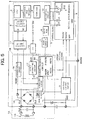
- FIG. 5 is a block diagram schematically showing an arrangement of a semiconductor circuit device according to the present embodiment.
- the semiconductor circuit device is integrated in an IC card including both functions of contact type and non-contact type IC cards and adopts a power-on reset circuit.
- the semiconductor circuit device generally includes an RF (Radio Frequency) section 1A (power obtaining section) which carries out communication using electromagnetic waves, a logic section 1B which includes a plurality of logic circuits performing various logical operations, a nonvolatile memory 8, and a voltage control circuit 9.
- the logic section 1B includes CPU (Central Processing Unit) 2 for data processing, a security processor 3 for performing a speedy encryption, a work RAM (Random Access Memory) 4 as a working region in an operating process, a boot ROM (Read Only Memory) 5 used on activation, a protocol control circuit 6, a reset circuit 7, CG (Clock Generator) 12, and a bus control circuit 10.
- CPU Central Processing Unit
- security processor 3 for performing a speedy encryption
- a work RAM Random Access Memory
- boot ROM Read Only Memory
- CG Circuit Generator
- the RF section 1A includes an antenna coil 13 for causing electromagnetic induction, a rectifying circuit 14 having connecting terminals of the antenna coil 13 and short key diodes, a modulation circuit 15, a demodulation circuit 16, a clock extracting circuit 17, and power-on reset circuit 18.
- the feature of the semiconductor circuit device is inclusion of the power-on reset circuit 18 as described below and the nonvolatile memory 8 having a large-capacity memory such as a flash memory.
- the nonvolatile memory 8 includes, for example, flash EEPROM (Electrically Erasable/Programmable Read Only Memory). Data writing and reading with respect to the nonvolatile memory 8 is carried out by the bus control circuit 10 in the logic section 1B. Note that, the nonvolatile memory 8 is not limited to the flash EEPROM, and any nonvolatile memories such as FeRAM and MRAM may be adopted.
- An electric power produced by electromagnetic induction is rectified by the rectifying circuit 14.
- REGIN voltage source as a power supply voltage, to which full-wave rectification is carried out by the rectifying circuit 14, is inputted to the voltage control circuit 9.
- An optimum voltage for each block is produced in the voltage control circuit 9 to be supplied to each block.
- waveforms of carrier waves from the rectifying circuit 14 are extracted by the clock extracting circuit 17 to produce clock signals.
- amplitude modulation is carried out by the modulation circuit 15 and the demodulation circuit 16 for data communication.
- the received signals are demodulated by the demodulation circuit 16.
- the demodulated signals are inputted via the selector circuit 11 to the protocol control circuit 6 and processed by the CPU 2.
- transmitter signals produced by the CPU 2 are inputted via the selector circuit 11 from the protocol control circuit 6 to the modulation circuit 15. After the transmitter signals are converted into appropriate signals for transmission in the modulation circuit 15, the converted signals are transmitted from the antenna coil 13.
- the IC card utilized in the present embodiment and the reader/writer apparatus corresponding to the IC card are defined to be based on type B standard of ISO/IEC 14443.
- the RF section 1A receives carrier waves having a frequency of 13.56 MHz transmitted by the reader/writer apparatus, and the modulation circuit 15 and the demodulation circuit 16 modulate and demodulate data which are superposed by the carrier waves amplitude-modulated by 10 % of ASK (Amplitude Shift Keying).
- the carrier waves transmitted from the reader/writer apparatus are received by the antenna coil 13 as adapted to be optimal for feeding power.
- Electric power activated by the antenna coil 13 is rectified by the rectifying circuit 14 that includes Schottky barrier diodes.
- Electrical signals produced in the rectifying circuit 14 are the following three signals: a CLK signal of 13.56 MHz extracted from the carrier waves in the clock extracting circuit 17; a data signal amplitude-modulated by 10% of ASK in the demodulation circuit 16; and power supply voltage (herein referred to as REGIN power voltage) to which full-wave rectification is carried out in the rectifying circuit 14.
- the waveforms of the voltages of REGIN power (REGIN voltage) and the VCC2V voltage are such waveforms as shown in Figure 11.
- the REGIN voltage rises in several tens of ⁇ sec after on-switch, and the rising waveform is sharp.
- chattering may occur at the time of a voltage rising. It is therefore necessary to set a reset period in the consideration of the occurrence of the chattering.
- the VCC2V voltage is a power supply voltage which is supplied to the logic section 1B and the nonvolatile memory 8 as well as output of a regulator constituting the voltage control circuit 9.
- reference voltage VREF is produced in a reference voltage producing circuit inside the voltage control circuit 9.
- the reference voltage VREF reaches an adequate voltage
- the VCC2V voltage is produced from the regulator. This is why there occurs the time difference between the risings of the REGIN voltage and the VCC2V voltage in Figure 11.
- the reference voltage VREF must be set to an optimum voltage value (for example, 1.5V) among from a GND level to a power supply voltage level.
- the waveforms of the REGIN voltage and the VCC2V voltage are such waveforms as shown in Figure 12.
- a rising period of the REGIN voltage is several hundreds of msec, and its rising waveform is gradual.
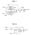
- the power-on reset circuit 18 can securely output and release the reset signal in either case of power voltage rising as described above. Referring to the block diagram of Figure 1, the power-on reset circuit 18 will be described in detail below.
- the power-on reset circuit 18 includes a first reset circuit 21, a second reset circuit 22, an NOR circuit (reset signal outputting circuit) 23, an NAND circuit 24, and an inverter 25.
- first reset circuit 21 the REGIN voltage, the VCC2V voltage, and the reference voltage VREF are supplied, and an RST1 signal (first reset signal) is outputted.
- RST1 signal first reset signal
- RST2 signal second reset signal
- the NOR circuit 23 outputs a result of a logical NOR operation with respect to the RST1 inputted from the first reset circuit 21 and the RST2 inputted from the second reset circuit 22. Further, the NAND circuit 24 outputs P-RSTB signal as a result of a logical NAND operation with respect to the input of the output from the NOR circuit 23 and the RSTB signal.
- the inverter 25 outputs a P-RST signal, which is an inverted version of the P-RSTB signal, as a power-on reset signal. Note that, the RSTB signal and the NAND circuit 24 will be described later.
- the first reset circuit 21 detects the rising of the VCC2V voltage using the reference voltage VREF as a standard so as to output the RST1 signal.
- the second reset circuit 22 detects the rising of the REGIN voltage using the reference voltage VREF as a standard so as to output the RST2 signal. This realizes a reset circuit available for both cases: a sharply rising voltage and a gradually rising voltage.
- the first reset circuit 21 and the second reset circuit 22 will be described in detail below.
- the first reset circuit 21 includes a comparator circuit 26 of which the power supply voltage is REGIN voltage, and an inverter 27.
- the VCC2V voltage is inputted to the (+) terminal of the comparator circuit 26 via a series-parallel circuit that includes a resistor R1 and a capacity C1. Further, the reference voltage VREF is inputted to the (-) terminal of the comparator circuit 26.
- the inverter 27 is provided for the determination of the polarity of the RST1 signal as a reset signal.
- output of the RST1 signal from the first reset circuit 21 is released after a delay of a time constant R1C1 by series-parallel circuit including the resistor R1 and the capacity C1 from a start of the output. Therefore, the time constant R1C1 is set so as to obtain the time for initialization of the system after the rising of the VCC2V voltage.
- the first reset circuit 21 is such a circuit as shown in Figure 11 that makes a response in case where the rising of the REGIN voltage is sharp. This will be described below.
- the rising of the REGIN voltage is sharp, the rising of the reference voltage VREF is fast and substantially equal to that of the REGIN voltage.
- Such a reference voltage VREF is inputted to the (-) terminal of the comparator circuit 26.
- the rising of the VCC2V voltage is little behind from that of the REGIN voltage.
- Such a VCC2V voltage is inputted to the (+) terminal of the comparator circuit 26 after the delay of the time constant R1C1 by the series-parallel circuit. That is, provision of the delay time by the time constant R1C1 secures the reset period.
- the (-) terminal voltage of the comparator circuit 26 to which a speedily rising reference voltage VREF is inputted is higher than the (+) terminal voltage to which the VCC2V voltage of which rising is little behind. Therefore, the RST1 signal outputted via the inverter 27 becomes "H” level. Thereafter, the VCC2V voltage increases after the delay time of the time constant R1C1. Along with this increase, the (+) terminal voltage rises, and the RST1 signal becomes "L” level at the point that the (+) terminal voltage is larger than the (-) terminal voltage.
- the period that the RST1 signal is in the "H” level is a reset period.
- the second reset circuit 22 includes a comparator circuit 28 of which the power supply voltage is REGIN voltage, and an inverter 29.
- the REGIN voltage which is divided at the resistors R3 and R4 is inputted to the (+) terminal of the comparator circuit 28 via a capacity C2 connected in parallel.
- the reference voltage VREF is inputted to the (-) terminal of the comparator circuit 28.
- the inverter 29 is provided for the determination of the polarity of the RST2 signal as a reset signal.
- the RST2 signal outputted from the second reset circuit 22 is outputted as a signal for releasing a reset state after the delay time of the time constant R4R3C2/(R4+R3) by the divided resistors R3 and R4 and a capacity C2 from the rising of the REGIN voltage. Therefore, the time constant R4R3C2/(R4+R3) is set so as to obtain the time for initialization of the system after the rising of the REGIN voltage.
- the second reset circuit 22 is such a circuit as shown in Figure 12 that makes a response in case where the rising of the REGIN voltage is gradual. This will be described below.
- the output of the reference voltage VREF follows the rising of the REGIN voltage. This is because the response of the reference voltage VREF is faster than the rising of the REGIN voltage.
- the VCC2V voltage is outputted from the regulator outputting circuit inside the voltage control circuit 9.
- the voltage divided at the resistors is inputted to the (+) terminal of the comparator circuit 28, so that the potential of the (+) terminal of the comparator circuit 28 is lower than that of the (-) terminal to which the reference voltage VREF is inputted. Therefore, the RST2 signal outputted via the inverter 29 becomes "H" level.
- the power-on reset circuit 18 includes the first reset circuit 21 and the second reset circuit 22 that perform the above operations.
- the power-on reset signal P-RST is obtained by the respective results of the RST1 signal and the RST2 signal by OR operation. That is, the power-on reset circuit 18 makes it possible to output the power-on reset signal P-RST which is capable of setting a suitable reset period whether the REGIN voltage rises sharply or gradually.
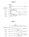
- a rising period tREGIN of the REGIN voltage is several ⁇ sec. That is, Figure 6 shows the case of a sharply rising REGIN voltage.
- the RST1 signal and the RST2 signal rise at the same timing of the rising of the REGIN voltage.
- the second reset circuit 22 detects the rising of the REGIN voltage, and the RST2 signal becomes "L” level.
- the RST1 signal becomes "L” level after a lapse of a reset period tRST1 which is determined by the delay time of the time constant R1C1 from the rising of the VCC2V voltage.
- the P-RST signal becomes "H”, and reset release is carried out.
- the first reset circuit 21 operates effectively.
- a rising period tREGIN of the REGIN voltage is several hundreds of msec. That is, Figure 7 shows the case where the REGIN voltage rises gradually.
- the reference voltage VREF rises in the same way.
- the VCC2V voltage starts to output.
- the first reset circuit 21 first detects the rising of the VCC2V voltage, and the RST1 signal is determined to be "L" level.
- the RST2 signal is outputted in the "H” level according to the rising of the REGIN voltage.
- the second reset circuit 22 detects that the REGIN voltage reaches the predetermined voltage (for example, about 4.0V)
- the RST2 signal is changed to the "L” level after a lapse of the delay time of the time constant R4R3C2/(R4+R3).
- the P-RST signal becomes "H", and reset release is carried out.
- the second reset circuit 22 effectively operates.
- the first reset circuit 21 and the second reset circuit 22 are designed in such a manner that the time range of their operation overlap each other for prevention of their malfunction. That is, it is designed in such a manner that the first reset circuit 21 operates in the range of the tREGIN period from several ⁇ sec to several msec, and the second reset circuit 22 operates in the range of the tREGIN period from several hundreds of ⁇ sec to several hundreds of msec. Switching of circuits is carried out in the tREGIN period of the range between several hundreds of ⁇ sec and several msec. In the range, both of the circuits operate; however, the second reset circuit 22 takes precedence over the first reset circuit 21.
- the RSTB signal (a third reset signal) is a reset signal supplied from outside.
- the NAND circuit 24 becomes active in response to the input of the reset signal of a logic level "L".
- the RSTB signal corresponds to the reset signal that is inputted from an external terminal of contact type.
- the RSTB signal as a reset signal from outside takes precedence over the RST1 signal and the RST2 signal.
- precedence with respect to these signals can be properly changed according to the specification of adopted IC cards. Change of the precedence can be possible by the change of the circuit corresponding to the NAND circuit 24.
- reset operation in a quick response to the input of the reset signal from external terminals can exclude effects caused by electromagnetic waves in the periphery devices including the reader/writer apparatus.
- FIG 4 shows an example of the arrangement of the second reset circuit 22 including such means for preventing malfunction of the reset signal.
- the second reset circuit 22 differs from an arrangement example of the second reset circuit 22 shown in Figure 3 in that a resistor R5 is provided between divided resistors R3 and R4 or a capacity C2, and the positive feedback is carried out via the resistor R6 from the output terminal to the (+) terminal of the comparator circuit 28. Any other arrangement is the same except for the above difference.
- Such a circuit which is called a hysteresis comparator, is useful for the provision of a hysteresis characteristic to the second reset circuit 22.
- Figure 8(a) shows an arrangement of a hysteresis comparator which includes the resistors R5 and R6 and an operational amplifier
- Figure 8(b) illustrate a waveform showing operation of the hysteresis comparator.
- Vr is a voltage supplied to the (+) terminal of the operational amplifier
- Vin is a voltage supplied to the (-) terminal of the same
- Vout is output from the operational amplifier.
- a horizontal axis shows a Vin
- a vertical axis shows Vout.
- VH R5 / (R5+R6) ⁇ (VoutH - Vr) + Vr
- VL R5 / (R5+R6) ⁇ (VoutL - Vr) + Vr
- setting of the resistors R5 and R6 can determine the upper limit voltage VH and the lower limit voltage VL.
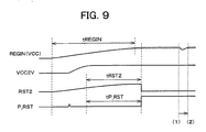
- Figure 9 illustrates waveforms showing operation of each signal in case of the second reset circuit 22 arranged as shown in Figure 4. Note that, Figure 9 shows an example of operations by the reset circuit in case where excessive current occurs inside the semiconductor circuit device. In Figure 9, it is assumed that excessive current occurs at the time period between (1) and (2), whereby the value of REGIN voltage decreases.
- provision of the hysteresis to the input section of the operational amplifier can absorb the variation of the REGIN voltage, so that it is possible to prevent the malfunction of the power-on reset circuit 18.
- a semiconductor circuit device for carrying out a RF power supply to the non-contact type IC card.
- any systems in which carries out the RF power supply other than the IC card can be applied to the present invention.
- non-contact tag system in which information is exchanged with a tag attached to a baggage without contacting.
- a power-on reset circuit provided in a system in which a power voltage is obtained from an external power supply source without contacting by electromagnetic induction, a power voltage thus obtained is converted into a predetermined voltage and supplied to a logic section which performs a logic operation, produces a reset signal for controlling a reset state of the system.
- the power-on reset circuit includes:
- the power-on reset circuit can be arranged so that the first reset circuit includes a comparator circuit for comparing the voltage supplied to the logic section and a reference voltage which is used in a regulator circuit for converting the output voltage of the rectifying circuit which rectifies the power voltage into a predetermined voltage, and produces the first reset signal in response to the comparator circuit.
- the first reset signal is produced in accordance with the result of the comparison between the reference voltage used in the regulator circuit and the voltage supplied to the logic section.
- the reference voltage which rises at the timing substantially same as that of the output voltage of the rectifying circuit, rises faster than the voltage supplied to the logic section. Therefore, according to the comparison between both voltages completely rising by an appropriate adjustment, the reference voltage is higher when the voltage supplied to the logic section does not rise. At the point that the voltage supplied to the logic section sufficiently rises, the voltage supplied to the logic section is higher. That is, according to the above arrangement, the rising of the voltage supplied to the logic section can be accurately detected by the relatively simple arrangement.
- the power-on reset circuit according to the present invention can be arranged so that the voltage supplied to the logic section is supplied to the comparator circuit via a delay circuit.
- the rising of the voltage supplied to the logic section is inputted to the comparator circuit after a delay by the delay circuit. That is, the rising of the voltage supplied to the logic section is detected after the delay time by the delay circuit from the actual rising. Therefore, setting the delay time so as to obtain the time required for system initialization can prevent malfunction in activating the system. Note that, the time required for system initialization is equivalent to the time period from the activation of the reset signal to the initialization of each peripheral block.
- the power-on reset circuit can be arranged so that the second reset circuit includes a comparator circuit for comparing the output voltage of the rectifying circuit and a reference voltage which is used in a regulator circuit for converting into a predetermined voltage the output voltage of the rectifying circuit which rectifies the power voltage, and produces the second reset signal in response to the comparator circuit.
- the second reset signal is produced in accordance with the result of the comparison between the reference voltage used in the regulator circuit and the output voltage of the rectifying circuit.
- the reference voltage rises at the timing substantially same as that of the output voltage of the rectifying circuit. Further, when the reference voltage completely rises, it is lower than the output voltage of the rectifying circuit. Therefore, according to the comparison between both voltages completely rising by an appropriate adjustment, the reference voltage is higher when the output voltage of the rectifying circuit does not rise. At the point that the output voltage of the rectifying circuit sufficiently rises, the output voltage of the rectifying circuit is higher. That is, according to the above arrangement, the rising of the output voltage of the rectifying circuit can be accurately detected by the relatively simple arrangement.
- the power-on reset circuit according to the present invention can be arranged so that the output voltage of the rectifying circuit is supplied to the comparator circuit via a delay circuit.
- the rising of the output voltage of the rectifying circuit is inputted to the comparator circuit after a delay by the delay circuit. That is, the rising of the output voltage of the rectifying circuit is detected after the delay time by the delay circuit from the actual rising. Therefore, setting the delay time so as to obtain the time required for system initialization can prevent malfunction in activating the system.
- the power-on reset circuit according to the present invention can be arranged so that the reset signal outputting circuit outputs the reset signal for releasing the reset state of the system when both the first and second reset signals become signals for releasing the reset state.
- the timing of the second reset signal becoming a signal for releasing the reset state is faster than that of the first resent signal becoming the same. Accordingly, a reset signal for releasing the reset state of the system is based on the first reset signal. That is, the reset release of the system is carried out in accordance with the first reset signal from the first reset circuit which surely carries out the reset release in case of a sharply rising power supply voltage.
- a reset signal for releasing the reset state of the system is based on the second reset signal. That is, the reset release of the system is carried out in accordance with the second reset signal from the second reset circuit which surely carries out the reset release in case of a gradually rising power supply voltage.
- the power-on reset circuit which can surely control the reset state of the system in both cases of a sharply rising power supply voltage and a gradually rising power supply voltage.
- the power-on reset circuit according to the present invention can be arranged so that the second reset circuit has a hysteresis characteristic with respect to variation in the output voltage of the rectifying circuit.
- the second reset circuit can change the production of the second reset signal in accordance with the variation of the output voltage of the rectifying circuit.
- the second reset circuit surely keeps the reset state when the power supply voltage rises.
- the hysteresis characteristic is set so that the second reset signal which releases the reset state is outputted at the point that the output voltage of the rectifying circuit completely rises.
- the variation of the output voltage of the rectifying circuit is in the downward direction when the output voltage of the rectifying circuit temporarily decreases due to a temporary increase in a consumed current in a state of the power supply voltage completely rising and being supplied in a steady manner.
- the hysteresis characteristic is set so that certain level of decrease in voltage cannot cause the shift to the reset state.
- the power-on reset circuit according to the present invention can be arranged so that the system performs a contact-type power supply from the external power supply source, the reset signal outputting circuit outputs as the reset signal one of the first reset signal, the second reset signal, and a third reset signal supplied along with the contact-type power supply.
- the above arrangement has a system in which non-contact and contact power supplies are carried out.
- the reset signal outputting circuit can output a reset signal in accordance with the third reset signal inputted along with contact-type power supply, in addition to the first and second reset signals. This makes it possible to provide the power-on reset circuit which can surely control the reset state of the system in either case of non-contact or contact power supply.
- the power-on reset circuit according to the present invention can be arranged so that the reset signal outputting circuit gives top priority outputting of the third reset signal as the reset signal when the third reset signal is supplied.
Landscapes
- Engineering & Computer Science (AREA)
- Theoretical Computer Science (AREA)
- Computer Hardware Design (AREA)
- Microelectronics & Electronic Packaging (AREA)
- Physics & Mathematics (AREA)
- General Physics & Mathematics (AREA)
- General Engineering & Computer Science (AREA)
- Computer Networks & Wireless Communication (AREA)
- Electronic Switches (AREA)
- Credit Cards Or The Like (AREA)
Abstract
Description
Further, electromagnetic induction makes it impossible to supply a large amount of electric power and causes variations in the amount of the power supply. Therefore, a power-on reset operation in starting the supply of power must be highly reliable.
Claims (18)
- A power-on reset circuit, provided in a system in which a power voltage is obtained from an external power supply source without contacting by electromagnetic induction, a power voltage thus obtained is converted into a predetermined voltage and supplied to a logic section (1B) which performs a logic operation, which produces a reset signal for controlling a reset state of the system,
the power-on reset circuit, characterized by comprising:a first reset circuit (21) for detecting a voltage supplied to the logic section (1B) so as to produce a first reset signal;a second reset circuit (22) for detecting an output voltage of a rectifying circuit (14) which rectifies a power voltage thus obtained from the external power supply source so as to produce a second reset signal; anda reset signal outputting circuit (23, 24, 25) for outputting as the reset signal either the first reset signal (21) or the second reset signal (22). - The power-on reset circuit according to claim 1, wherein the first reset circuit (21) includes a comparator circuit (26) for comparing the voltage supplied to the logic section (1B) and a reference voltage which is used in a regulator circuit (9) for converting the output voltage of the rectifying circuit (14) which rectifies the power voltage into a predetermined voltage, and produces the first reset signal in response to the comparator circuit (26).
- The power-on reset circuit according to claim 2, wherein the voltage supplied to the logic section (1B) is supplied to the comparator circuit (26) via a delay circuit (R1, C1).
- The power-on reset circuit according to claim 3, wherein the delay circuit (R1, C1) includes a resistor (R1) and a capacitor (C1).
- The power-on reset circuit according to any one of claims 1 to 4, wherein the second reset circuit (22) includes a comparator circuit (28) for comparing the output voltage of the rectifying circuit (14) and a reference voltage which is used in a regulator circuit (9) for converting into a predetermined voltage the output voltage of the rectifying circuit (14) which rectifies the power voltage, and produces the second reset signal in response to the comparator circuit (28).
- The power-on reset circuit according to claim 5, wherein the output voltage of the rectifying circuit (14) is supplied to the comparator circuit (28) via a delay circuit (R3, R4, C2).
- The power-on reset circuit according to claim 6, wherein the delay circuit (28) includes a resistor (R3, R4) and a capacitor (C2).
- The power-on reset circuit according to any one of claims 1 to 7, wherein the reset signal outputting circuit (23) outputs the reset signal for releasing the reset state of the system when both the first and second reset signals become signals for releasing the reset state.
- The power-on reset circuit according to claim 8, wherein the reset signal outputting circuit (23) conducts a logical NOR operation with respect to the first and second reset signals so as to output the reset signal.
- The power-on reset circuit according to any one of claims 1 to 9, wherein the second reset circuit (22) has a hysteresis characteristic with respect to variation in the output voltage of the rectifying circuit (14).
- The power-on reset circuit according to any one of claims 1 to 10, wherein the system also performs a contact-type power supply from the external power supply source, the reset signal outputting circuit (24) outputs as the reset signal one of the first reset signal, the second reset signal, and a third reset signal supplied along with the contact-type power supply.
- The power-on reset circuit according to claim 11, wherein the reset signal outputting circuit (24) gives top priority outputting of the third reset signal as the reset signal when the third reset signal is supplied.
- An IC apparatus, comprising:wherein the power-on reset circuit (18) includes:(a) a power source obtaining section (1A) for obtaining a power voltage from an external power supply source without contacting by electromagnetic induction;(b) a voltage control circuit (9) for converting a power voltage thus obtained from the power source obtaining section (1A) into a predetermined voltage;(c) a logic section (1B) for being supplied voltage from the voltage control circuit (9) and for conducting a logical operation; and(d) a power-on reset circuit (18) for producing a reset signal for controlling a reset state of the logic section,a first reset circuit (21) for detecting a voltage supplied to the logic section (1B) so as to produce a first reset signal;a second reset circuit (22) for detecting an output voltage of a rectifying circuit (14) which rectifies a power voltage thus obtained from the external power supply source so as to produce a second reset signal; anda reset signal outputting circuit (23, 24, 25) for outputting as the reset signal either the first reset signal or the second reset signal.
- The IC apparatus according to claim 13, further comprising a nonvolatile memory (8) to and from which the logic section (1B) can write and read information.
- The IC apparatus according to claim 13 or claim 14, wherein the power source obtaining section (1A) demodulates data superposed by electromagnetic waves transmitted from the external power supply source, and modulates data transmitted from the logic section (1B) to transmit electromagnetic waves toward outside.
- The IC apparatus according to claim 13, 14, or 15, wherein the power source obtaining section (1A) extracts a clock signal superposed by electromagnetic waves transmitted from the external power supply source, and transmits a clock signal thus extracted to the logic section (1B).
- The IC apparatus according to any one of claims 13 to 16, wherein the power source obtaining section (1A), the voltage control circuit (9), the logic section (1B), and the power-on reset circuit (18) are included inside a card object.
- The IC apparatus according to any one of claims 13 to 17, wherein the power source obtaining section (1A) is also arranged so as to perform a contact-type power supply from the external power supply source.
Priority Applications (1)
| Application Number | Priority Date | Filing Date | Title |
|---|---|---|---|
| EP07014761A EP1845480A3 (en) | 2001-07-30 | 2002-07-30 | Power-on reset circuit for an IC card |
Applications Claiming Priority (2)
| Application Number | Priority Date | Filing Date | Title |
|---|---|---|---|
| JP2001230490 | 2001-07-30 | ||
| JP2001230490A JP3904859B2 (en) | 2001-07-30 | 2001-07-30 | Power-on reset circuit and IC card having the same |
Related Child Applications (1)
| Application Number | Title | Priority Date | Filing Date |
|---|---|---|---|
| EP07014761A Division EP1845480A3 (en) | 2001-07-30 | 2002-07-30 | Power-on reset circuit for an IC card |
Publications (3)
| Publication Number | Publication Date |
|---|---|
| EP1282071A2 true EP1282071A2 (en) | 2003-02-05 |
| EP1282071A3 EP1282071A3 (en) | 2003-09-10 |
| EP1282071B1 EP1282071B1 (en) | 2008-02-20 |
Family
ID=19062693
Family Applications (2)
| Application Number | Title | Priority Date | Filing Date |
|---|---|---|---|
| EP02255330A Expired - Lifetime EP1282071B1 (en) | 2001-07-30 | 2002-07-30 | Power-on reset circuit for an IC card |
| EP07014761A Withdrawn EP1845480A3 (en) | 2001-07-30 | 2002-07-30 | Power-on reset circuit for an IC card |
Family Applications After (1)
| Application Number | Title | Priority Date | Filing Date |
|---|---|---|---|
| EP07014761A Withdrawn EP1845480A3 (en) | 2001-07-30 | 2002-07-30 | Power-on reset circuit for an IC card |
Country Status (7)
| Country | Link |
|---|---|
| US (1) | US6737884B2 (en) |
| EP (2) | EP1282071B1 (en) |
| JP (1) | JP3904859B2 (en) |
| KR (1) | KR100507252B1 (en) |
| CN (1) | CN1224881C (en) |
| DE (1) | DE60225093T2 (en) |
| TW (1) | TW564594B (en) |
Cited By (5)
| Publication number | Priority date | Publication date | Assignee | Title |
|---|---|---|---|---|
| WO2004098058A1 (en) * | 2003-05-02 | 2004-11-11 | Potentia Semiconductor, Inc. | Power-on reset circuit |
| EP1672388A1 (en) | 2004-12-20 | 2006-06-21 | St Microelectronics S.A. | Electromagnetic transponder without autonomous energy supply |
| US7218204B2 (en) | 2003-08-18 | 2007-05-15 | Matsushita Electric Industrial Co., Ltd. | Contactless IC card |
| EP1496436A3 (en) * | 2003-07-07 | 2008-11-05 | STMicroelectronics, Inc. | Method and apparatus for autoreset of a usb smart card device in a mute mode |
| EP3331123A1 (en) * | 2016-12-05 | 2018-06-06 | Cal-Comp Big Data, Inc. | Electronic apparatus and power supply circuit thereof |
Families Citing this family (41)
| Publication number | Priority date | Publication date | Assignee | Title |
|---|---|---|---|---|
| ITRM20010522A1 (en) * | 2001-08-30 | 2003-02-28 | Micron Technology Inc | CONDITIONED AND STURDY "POWER-ON-RESET" SEQUENTIAL WITH ULTRA-LOW POWER FOR INTEGRATED CIRCUITS. |
| FR2835328B1 (en) * | 2002-01-31 | 2005-04-08 | St Microelectronics Sa | CIRCUIT FOR STARTING AND PROTECTING AGAINST FAULT VOLTAGES FOR A CONTACTLESS CIRCUIT |
| KR20030079442A (en) * | 2002-04-04 | 2003-10-10 | 삼성전자주식회사 | Multi sequence reset circuit |
| US6711062B1 (en) * | 2002-07-17 | 2004-03-23 | Taiwan Semiconductor Manufacturing Company | Erase method of split gate flash memory reference cells |
| KR100919980B1 (en) * | 2003-01-18 | 2009-10-05 | 삼성디지털이미징 주식회사 | Power supply with stable reset function in portable electronic devices |
| JP4140420B2 (en) * | 2003-03-28 | 2008-08-27 | ミツミ電機株式会社 | Semiconductor device and reset signal transmission method |
| KR100562501B1 (en) * | 2003-05-02 | 2006-03-21 | 삼성전자주식회사 | Power-on initialization circuit and semiconductor integrated circuit device comprising same |
| JP3863508B2 (en) * | 2003-07-03 | 2006-12-27 | Necエレクトロニクス株式会社 | Power supply voltage detection circuit and semiconductor integrated circuit device |
| FR2864296B1 (en) * | 2003-12-17 | 2006-04-28 | Gemplus Card Int | IMMUNITY TO VARIATIONS IN LIMITED RESOURCES, PROVIDED TO A DUAL INTERFACE OBJECT |
| JP4519476B2 (en) * | 2004-02-03 | 2010-08-04 | 株式会社東芝 | Wireless communication device |
| DE102004014203B4 (en) * | 2004-03-23 | 2006-02-02 | Infineon Technologies Ag | Contactless data carrier with current demodulation |
| JP4096315B2 (en) * | 2004-08-04 | 2008-06-04 | セイコーエプソン株式会社 | Display system |
| JP4618672B2 (en) * | 2004-09-02 | 2011-01-26 | フェリカネットワークス株式会社 | Semiconductor integrated circuit and wireless communication device |
| TWI270782B (en) * | 2004-11-05 | 2007-01-11 | Via Tech Inc | Rebooting card and its method for determining a timing of restarting a reset mechanism |
| JP4437541B2 (en) * | 2004-11-17 | 2010-03-24 | 富士通マイクロエレクトロニクス株式会社 | Reset control circuit and reset control method |
| US7242218B2 (en) * | 2004-12-02 | 2007-07-10 | Altera Corporation | Techniques for combining volatile and non-volatile programmable logic on an integrated circuit |
| KR100583611B1 (en) * | 2005-01-25 | 2006-05-26 | 삼성전자주식회사 | Power-On Reset Circuit and Power-On Reset Method |
| US8395426B2 (en) * | 2005-05-19 | 2013-03-12 | Broadcom Corporation | Digital power-on reset controller |
| CN1959595A (en) * | 2005-11-04 | 2007-05-09 | 鸿富锦精密工业(深圳)有限公司 | Reset circuit of computer system |
| KR100684907B1 (en) * | 2006-01-09 | 2007-02-22 | 삼성전자주식회사 | Multi-Chip Package Reduces Peak Current During Power-Up |
| JP4345770B2 (en) * | 2006-04-11 | 2009-10-14 | エルピーダメモリ株式会社 | Latch circuit and semiconductor device having the same |
| JP4800421B2 (en) * | 2006-10-12 | 2011-10-26 | エヌエックスピー ビー ヴィ | Device, system and method for compensating signal delays in an RFID communication system |
| CN100498649C (en) * | 2007-03-28 | 2009-06-10 | 威盛电子股份有限公司 | Reset system and reset method |
| US7417476B1 (en) * | 2007-04-24 | 2008-08-26 | Smartech Worldwide Limited | Power-on-reset circuit with output reset to ground voltage during power off |
| EP3258536A1 (en) * | 2007-09-19 | 2017-12-20 | Qualcomm Incorporated | Maximizing power yield from wireless power magnetic resonators |
| JP4268655B1 (en) * | 2007-11-19 | 2009-05-27 | シャープ株式会社 | Power-on reset circuit and combination IC card |
| KR100937948B1 (en) * | 2008-06-04 | 2010-01-21 | 주식회사 하이닉스반도체 | Power-Up Signal Generation Circuit and Generation Method |
| US7952402B2 (en) * | 2009-02-06 | 2011-05-31 | Standard Microsystems Corporation | Power-up control for very low-power systems |
| US8493109B2 (en) | 2010-03-31 | 2013-07-23 | Qualcomm Incorporated | System and method to control a power on reset signal |
| KR101646910B1 (en) * | 2011-01-11 | 2016-08-09 | 페어차일드코리아반도체 주식회사 | Semiconductor device including power on reset circuit |
| KR101321285B1 (en) * | 2011-09-05 | 2013-10-28 | 삼성전기주식회사 | Apparatus for realizing reset using enable signal |
| US8981823B1 (en) | 2011-09-29 | 2015-03-17 | Spansion Llc | Apparatus and method for smart VCC trip point design for testability |
| US8536908B2 (en) * | 2011-09-29 | 2013-09-17 | Spansion Llc | Apparatus and method for smart VCC trip point design for testability |
| JP5852538B2 (en) | 2012-09-26 | 2016-02-03 | ルネサスエレクトロニクス株式会社 | Semiconductor device |
| JP5985949B2 (en) * | 2012-10-01 | 2016-09-06 | ローム株式会社 | Timer circuit, and power-on reset circuit, electronic device and vehicle using the same |
| JP6057665B2 (en) * | 2012-10-25 | 2017-01-11 | ローム株式会社 | Semiconductor devices, electronic devices, vehicles |
| KR101405905B1 (en) | 2012-11-27 | 2014-06-12 | 현대오트론 주식회사 | Method for avoiding unwanted reset in two IC having different power on reset voltage range |
| DE102016102696A1 (en) * | 2016-02-16 | 2017-08-17 | Infineon Technologies Ag | Apparatus and method for internal reset signal generation |
| JP6870962B2 (en) * | 2016-11-25 | 2021-05-12 | ラピスセミコンダクタ株式会社 | Semiconductor devices, communication devices and reset methods |
| KR102810181B1 (en) * | 2020-09-29 | 2025-05-20 | 삼성전자주식회사 | Method of resetting storage device and storage device performing the same |
| EP4380055A1 (en) | 2022-11-30 | 2024-06-05 | Stichting IMEC Nederland | A power-on reset circuitry, an implant device and a method for generating a power-on reset signal |
Family Cites Families (18)
| Publication number | Priority date | Publication date | Assignee | Title |
|---|---|---|---|---|
| US4798978A (en) * | 1987-04-30 | 1989-01-17 | Gain Electronics Corporation | GAAS FET logic having increased noise margin |
| JPH04265012A (en) * | 1991-02-20 | 1992-09-21 | Mitsubishi Electric Corp | Power-on resetting circuit |
| JP2797844B2 (en) * | 1992-06-17 | 1998-09-17 | 三菱電機株式会社 | Semiconductor integrated circuit |
| JPH0877318A (en) * | 1994-09-08 | 1996-03-22 | Toshiba Corp | Non-contact type information recording medium |
| KR0177093B1 (en) * | 1995-05-31 | 1999-05-15 | 윤종용 | CPU reset circuit |
| JP3650186B2 (en) * | 1995-11-28 | 2005-05-18 | 株式会社ルネサステクノロジ | Semiconductor device and comparison circuit |
| JP3360002B2 (en) * | 1996-03-14 | 2002-12-24 | 沖電気工業株式会社 | Contact / non-contact IC card and contact / non-contact IC card reader / writer |
| JPH1078834A (en) * | 1996-09-04 | 1998-03-24 | Seiko Epson Corp | Power supply voltage detection circuit and IC card having the same |
| JPH10162108A (en) * | 1996-11-29 | 1998-06-19 | Tokimec Inc | Data storage |
| US5831460A (en) * | 1997-02-26 | 1998-11-03 | Xilinx, Inc. | Power-on reset circuit with separate power-up and brown-out trigger levels |
| JPH10269327A (en) * | 1997-03-27 | 1998-10-09 | Hitachi Ltd | Control circuit |
| US6085342A (en) * | 1997-05-06 | 2000-07-04 | Telefonaktiebolaget L M Ericsson (Publ) | Electronic system having a chip integrated power-on reset circuit with glitch sensor |
| JP2000040950A (en) * | 1998-07-23 | 2000-02-08 | Seiko Epson Corp | Reset signal release circuit |
| KR100328825B1 (en) * | 1999-07-09 | 2002-03-14 | 박종섭 | Error prevention circuit |
| DE10024980B4 (en) * | 2000-05-19 | 2006-03-23 | Atmel Germany Gmbh | Method for switching transistors at low voltages |
| JP3820913B2 (en) * | 2001-05-16 | 2006-09-13 | ヤマハ株式会社 | Power on / off reset circuit |
| US6437614B1 (en) * | 2001-05-24 | 2002-08-20 | Sunplus Technology Co., Ltd. | Low voltage reset circuit device that is not influenced by temperature and manufacturing process |
| US6683478B2 (en) * | 2001-11-13 | 2004-01-27 | Samsung Electronics Co., Ltd. | Apparatus for ensuring correct start-up and phase locking of delay locked loop |
-
2001
- 2001-07-30 JP JP2001230490A patent/JP3904859B2/en not_active Expired - Fee Related
-
2002
- 2002-07-29 TW TW091116862A patent/TW564594B/en not_active IP Right Cessation
- 2002-07-30 US US10/207,187 patent/US6737884B2/en not_active Expired - Lifetime
- 2002-07-30 KR KR10-2002-0044843A patent/KR100507252B1/en not_active Expired - Fee Related
- 2002-07-30 CN CNB021318956A patent/CN1224881C/en not_active Expired - Lifetime
- 2002-07-30 EP EP02255330A patent/EP1282071B1/en not_active Expired - Lifetime
- 2002-07-30 EP EP07014761A patent/EP1845480A3/en not_active Withdrawn
- 2002-07-30 DE DE60225093T patent/DE60225093T2/en not_active Expired - Lifetime
Cited By (6)
| Publication number | Priority date | Publication date | Assignee | Title |
|---|---|---|---|---|
| WO2004098058A1 (en) * | 2003-05-02 | 2004-11-11 | Potentia Semiconductor, Inc. | Power-on reset circuit |
| EP1496436A3 (en) * | 2003-07-07 | 2008-11-05 | STMicroelectronics, Inc. | Method and apparatus for autoreset of a usb smart card device in a mute mode |
| US7218204B2 (en) | 2003-08-18 | 2007-05-15 | Matsushita Electric Industrial Co., Ltd. | Contactless IC card |
| EP1672388A1 (en) | 2004-12-20 | 2006-06-21 | St Microelectronics S.A. | Electromagnetic transponder without autonomous energy supply |
| EP3331123A1 (en) * | 2016-12-05 | 2018-06-06 | Cal-Comp Big Data, Inc. | Electronic apparatus and power supply circuit thereof |
| US10348113B2 (en) | 2016-12-05 | 2019-07-09 | Cal-Comp Big Data, Inc. | Power supply circuit with reset function and electronic apparatus having the same |
Also Published As
| Publication number | Publication date |
|---|---|
| EP1282071A3 (en) | 2003-09-10 |
| DE60225093T2 (en) | 2009-02-19 |
| JP2003044176A (en) | 2003-02-14 |
| CN1224881C (en) | 2005-10-26 |
| EP1845480A2 (en) | 2007-10-17 |
| DE60225093D1 (en) | 2008-04-03 |
| US6737884B2 (en) | 2004-05-18 |
| TW564594B (en) | 2003-12-01 |
| CN1400516A (en) | 2003-03-05 |
| EP1282071B1 (en) | 2008-02-20 |
| EP1845480A3 (en) | 2009-08-26 |
| KR20030011676A (en) | 2003-02-11 |
| KR100507252B1 (en) | 2005-08-11 |
| US20030020525A1 (en) | 2003-01-30 |
| JP3904859B2 (en) | 2007-04-11 |
Similar Documents
| Publication | Publication Date | Title |
|---|---|---|
| US6737884B2 (en) | Power-on reset circuit and IC card | |
| KR100275167B1 (en) | Chip card with field strength detector | |
| US7145960B2 (en) | Transmitter apparatus and communication system employing the same | |
| KR101689051B1 (en) | Rfid reading device, rfid system, method for controlling the transmitting power of an rfid reading device, and computer program product | |
| JP3967487B2 (en) | IC card | |
| US6848620B2 (en) | Semiconductor integrated circuit | |
| JPWO1993011509A1 (en) | Data carrier | |
| EP1742172B1 (en) | Semiconductor integrated circuit and contactless type information system including the same | |
| US7681060B2 (en) | Semiconductor integrated circuit device and IC card equipped with the same having transistor switch for disconnecting contact power during contactless mode | |
| US20060022798A1 (en) | Reader/writer for transmitting command to IC tag, communication method and communication system based thereon | |
| TWI382303B (en) | Power supply reset circuit and combination IC card | |
| CN109426847B (en) | Power supply method and electronic card using same | |
| US11599759B2 (en) | Passive RFID tag and RFID system | |
| KR100874983B1 (en) | Tag chip and its driving method | |
| US20080100415A1 (en) | Data carrier and data carrier system | |
| JP3904860B2 (en) | Power supply device, semiconductor circuit device, and IC card | |
| KR200324928Y1 (en) | Card Reader Switched by Capacitive Sensor | |
| JP2007257543A (en) | Composite portable electronic device and composite IC card | |
| JP2009295046A (en) | Contactless ic card, communication method, program, and communication system | |
| JP2007133734A (en) | Semiconductor integrated circuit and non-contact information medium |
Legal Events
| Date | Code | Title | Description |
|---|---|---|---|
| PUAI | Public reference made under article 153(3) epc to a published international application that has entered the european phase |
Free format text: ORIGINAL CODE: 0009012 |
|
| AK | Designated contracting states |
Designated state(s): AT BE BG CH CY CZ DE DK EE ES FI FR GB GR IE IT LI LU MC NL PT SE SK TR |
|
| AX | Request for extension of the european patent |
Extension state: AL LT LV MK RO SI |
|
| PUAL | Search report despatched |
Free format text: ORIGINAL CODE: 0009013 |
|
| AK | Designated contracting states |
Kind code of ref document: A3 Designated state(s): AT BE BG CH CY CZ DE DK EE ES FI FR GB GR IE IT LI LU MC NL PT SE SK TR |
|
| AX | Request for extension of the european patent |
Extension state: AL LT LV MK RO SI |
|
| RIC1 | Information provided on ipc code assigned before grant |
Ipc: 7G 06F 1/26 B Ipc: 7G 06F 1/24 B Ipc: 7H 03K 17/22 B Ipc: 7H 03K 3/356 B Ipc: 7G 05F 1/46 B Ipc: 7G 06K 19/07 A Ipc: 7G 01R 19/155 B |
|
| 17P | Request for examination filed |
Effective date: 20031201 |
|
| 17Q | First examination report despatched |
Effective date: 20040122 |
|
| AKX | Designation fees paid |
Designated state(s): DE FR GB |
|
| 17Q | First examination report despatched |
Effective date: 20040122 |
|
| 17Q | First examination report despatched |
Effective date: 20040122 |
|
| GRAP | Despatch of communication of intention to grant a patent |
Free format text: ORIGINAL CODE: EPIDOSNIGR1 |
|
| GRAS | Grant fee paid |
Free format text: ORIGINAL CODE: EPIDOSNIGR3 |
|
| GRAA | (expected) grant |
Free format text: ORIGINAL CODE: 0009210 |
|
| AK | Designated contracting states |
Kind code of ref document: B1 Designated state(s): DE FR GB |
|
| REG | Reference to a national code |
Ref country code: GB Ref legal event code: FG4D |
|
| REF | Corresponds to: |
Ref document number: 60225093 Country of ref document: DE Date of ref document: 20080403 Kind code of ref document: P |
|
| ET | Fr: translation filed | ||
| PLBE | No opposition filed within time limit |
Free format text: ORIGINAL CODE: 0009261 |
|
| STAA | Information on the status of an ep patent application or granted ep patent |
Free format text: STATUS: NO OPPOSITION FILED WITHIN TIME LIMIT |
|
| 26N | No opposition filed |
Effective date: 20081121 |
|
| REG | Reference to a national code |
Ref country code: FR Ref legal event code: TP Owner name: INTELLECTUAL PROPERTIES 1 KFT., HU Effective date: 20120125 |
|
| REG | Reference to a national code |
Ref country code: DE Ref legal event code: R082 Ref document number: 60225093 Country of ref document: DE Representative=s name: PATENTANWAELTE RUFF, WILHELM, BEIER, DAUSTER &, DE |
|
| REG | Reference to a national code |
Ref country code: GB Ref legal event code: 732E Free format text: REGISTERED BETWEEN 20120426 AND 20120502 |
|
| REG | Reference to a national code |
Ref country code: DE Ref legal event code: R081 Ref document number: 60225093 Country of ref document: DE Owner name: SAMSUNG ELECTRONICS CO., LTD., SUWON-SI, KR Free format text: FORMER OWNER: SHARP K.K., OSAKA, JP Effective date: 20120330 Ref country code: DE Ref legal event code: R082 Ref document number: 60225093 Country of ref document: DE Representative=s name: PATENTANWAELTE RUFF, WILHELM, BEIER, DAUSTER &, DE Effective date: 20120330 Ref country code: DE Ref legal event code: R081 Ref document number: 60225093 Country of ref document: DE Owner name: INTELLECTUAL PROPERTIES I KFT., HU Free format text: FORMER OWNER: SHARP K.K., OSAKA, JP Effective date: 20120330 |
|
| REG | Reference to a national code |
Ref country code: DE Ref legal event code: R082 Ref document number: 60225093 Country of ref document: DE Representative=s name: PATENTANWAELTE RUFF, WILHELM, BEIER, DAUSTER &, DE |
|
| REG | Reference to a national code |
Ref country code: DE Ref legal event code: R081 Ref document number: 60225093 Country of ref document: DE Owner name: SAMSUNG ELECTRONICS CO., LTD., SUWON-SI, KR Free format text: FORMER OWNER: INTELLECTUAL PROPERTIES I KFT., BUDAPEST, HU Effective date: 20150203 Ref country code: DE Ref legal event code: R082 Ref document number: 60225093 Country of ref document: DE Representative=s name: PATENTANWAELTE RUFF, WILHELM, BEIER, DAUSTER &, DE Effective date: 20150203 |
|
| REG | Reference to a national code |
Ref country code: GB Ref legal event code: 732E Free format text: REGISTERED BETWEEN 20150226 AND 20150304 |
|
| REG | Reference to a national code |
Ref country code: FR Ref legal event code: TP Owner name: SAMSUNG ELECTRONICS CO., LTD., KR Effective date: 20150421 |
|
| REG | Reference to a national code |
Ref country code: FR Ref legal event code: PLFP Year of fee payment: 15 |
|
| REG | Reference to a national code |
Ref country code: FR Ref legal event code: PLFP Year of fee payment: 16 |
|
| REG | Reference to a national code |
Ref country code: FR Ref legal event code: PLFP Year of fee payment: 17 |
|
| PGFP | Annual fee paid to national office [announced via postgrant information from national office to epo] |
Ref country code: FR Payment date: 20210611 Year of fee payment: 20 |
|
| PGFP | Annual fee paid to national office [announced via postgrant information from national office to epo] |
Ref country code: DE Payment date: 20210630 Year of fee payment: 20 Ref country code: GB Payment date: 20210701 Year of fee payment: 20 |
|
| REG | Reference to a national code |
Ref country code: DE Ref legal event code: R071 Ref document number: 60225093 Country of ref document: DE |
|
| REG | Reference to a national code |
Ref country code: GB Ref legal event code: PE20 Expiry date: 20220729 |
|
| PG25 | Lapsed in a contracting state [announced via postgrant information from national office to epo] |
Ref country code: GB Free format text: LAPSE BECAUSE OF EXPIRATION OF PROTECTION Effective date: 20220729 |