EP1278138A2 - Verfahren, durch welches basierend auf dem Schaltplan einer digitalen Schaltung der im Betrieb der digitalen Schaltung von dieser gezogene Strom ermittelbar ist - Google Patents
Verfahren, durch welches basierend auf dem Schaltplan einer digitalen Schaltung der im Betrieb der digitalen Schaltung von dieser gezogene Strom ermittelbar ist Download PDFInfo
- Publication number
- EP1278138A2 EP1278138A2 EP02015843A EP02015843A EP1278138A2 EP 1278138 A2 EP1278138 A2 EP 1278138A2 EP 02015843 A EP02015843 A EP 02015843A EP 02015843 A EP02015843 A EP 02015843A EP 1278138 A2 EP1278138 A2 EP 1278138A2
- Authority
- EP
- European Patent Office
- Prior art keywords
- circuit
- inverter
- replaced
- replacement
- change
- Prior art date
- Legal status (The legal status is an assumption and is not a legal conclusion. Google has not performed a legal analysis and makes no representation as to the accuracy of the status listed.)
- Withdrawn
Links
Images

Classifications
-
- G—PHYSICS
- G06—COMPUTING OR CALCULATING; COUNTING
- G06F—ELECTRIC DIGITAL DATA PROCESSING
- G06F30/00—Computer-aided design [CAD]
- G06F30/30—Circuit design
- G06F30/32—Circuit design at the digital level
- G06F30/33—Design verification, e.g. functional simulation or model checking
Definitions
- the present invention relates to a method according to the Preamble of claim 1, i.e. a process by which is based on the circuit diagram of a digital circuit the one pulled by the digital circuit during operation Electricity can be determined.
- the digital circuit is part of an integrated Circuit
- preventive measures of malfunctions for example in that in the integrated Circuit filters are integrated, which prevents is that the one drawn by the digital circuit Current causes fluctuations in the supply voltage which the digital circuit and / or other components of the the system containing the digital circuit is powered become.
- the optimal dimensioning of these filters depends on the Size of flowing currents, particularly the size of the maximum current.
- the filters have been dimensioned on the basis of Experience. It is not uncommon for the Sizing significantly from the optimal sizing differs. This means that the filter is often considerably oversized or significantly undersized.
- the filter If the filter is undersized, it will be replaced by the Filters to avoid supply voltage fluctuations not avoided or not sufficiently avoided.
- the filter is oversized, the integrated one Circuit, more precisely the semiconductor chip carrying this bigger than is necessary.
- the essential components the filter is namely one or more capacitors, and their implementation in an integrated circuit requires relatively much chip area. The larger the integrated circuit becomes, the more expensive it becomes, although because of the large Quantity in which integrated circuits are manufactured become, even small increases in price considerable additional costs cause.
- Such Circuits can be back-annotated using their Network list can be simulated.
- the network list gives the circuit diagram the digital circuit to be realized again. It contains a list of the components that the circuit in question contains, and their interconnection.
- This netlist is used for creation the layout of the digital circuit in question containing integrated circuit used.
- the back annotated Netlist also contains information about existing parasitic capacitances, inductances and resistances, with which in the practical implementation of the underlying digital circuit is to be expected. Based can be determined in detail on the back-listed network list be how the digital circuitry works during operation the same will behave. It can also be determined which currents flow with which input signals.
- the present invention is therefore based on the object to find a way to distinguish yourself from a digital circuit drawn current when designing the same can be determined easily, quickly and precisely.
- the inventive method is characterized in that the determination of the current using an equivalent circuit takes place in which circuit parts of the digital Circuit whose output signal levels change simultaneously or change, are replaced by an inverter.
- This simple construction of the equivalent circuit allows the through this flowing current, and thus also through that digital circuit flowing current even with conventional Methods for determining a current from a circuit diagram can be determined easily, quickly and precisely.
- the digital circuit for which based on the circuit diagram the same as that pulled by it in practical use Current to be determined is in the example considered a synchronously clocked digital circuit, more precisely a microcontroller or a part (a specific module) of a microcontroller.
- a digital circuit can therefore be divided by a number of described in the following as a replacement inverter of which a part switches from 0 to 1, and the rest from 1 to 0.
- circuit parts in which the digital circuit in the first Step is partitioned with circuit parts one or more input connections and one or several output connections.
- circuit parts that like logic gates for example AND gates, OR gates, NAND gates, NOR gates, Represent XOR gates, inverters etc. It is already pointed out at this point that the mentioned circuit parts also larger circuit parts (for example circuit parts representing several gates) or smaller circuit parts (e.g. only a part circuit parts representing a gate).
- Circuit diagram containing circuit parts e.g. a Circuit diagram in the manner of FIG. 1 described later shown circuit diagram
- the first step can of course also be dispensed with.
- the logical depth indicates how many in a row switched circuit parts a respective circuit part with a clock signal connection of the digital circuit is connected, via which the digital circuit Timing-controlling clock signal is supplied.
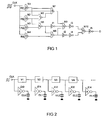
- the determination of the logical depth is based on the following of Figure 1 explained.
- the arrangement shown in Figure 1 consists of NAND gates N1 to N10 and inverters I1 to I5, which are connected as shown in FIG. 1.
- the NAND gates and inverters are circuit parts that, like later is described in more detail, replace with replacement inverter to let; the arrangement is one after implementation arrangement obtained from the above first step.
- the arrangement has input terminals IN1 to IN4, one Output terminal O, and a clock signal input terminal CLK on which a clock signal is supplied to the arrangement.
- the logical depth 0 is assigned to the NAND gates N1 to N4, because one of their input ports is direct is connected to the clock signal terminal CLK.
- the logical depth 0 is assigned to the NAND gate N7 because the input connection of the same, the least one after the other arranged other gates are connected upstream, over none another gate, i.e. directly with the clock signal connection CLK connected is. That at the same time the other input connections of the NAND gate N7 via the NAND gate N1 or via the NAND gates N1 and N5 or via the NAND gates N2 and N5 are connected to the clock signal terminal CLK no role, because in the example considered only the shortest Connections to the clock signal connection CLK are taken into account.
- the logical depth 1 is assigned to the NAND gates N5 and N6, because their input ports are over another Gate, more precisely via the NAND gate N1 or the NAND gate N2 (input connections from N5) or via the NAND gate N2 or the NAND gate N3 (input connections of N6) are connected to the clock signal terminal CLK.
- the logical depth 2 is assigned to the inverter I1 because of the The input connection of the same via two consecutively arranged other gates, more precisely via the NAND gates N2 and N6 or via the NAND gates N3 and N6 with the clock signal connection CLK is connected.
- Logical depth 1 is assigned to NAND gate N8 because the input connection of the same, the least one after the other arranged other gates are connected upstream via a other gate, more precisely via gate N4 with the Clock signal terminal CLK is connected.
- Logical depth 1 is assigned to NAND gate N9 because the input connection of the same, the least one after the other arranged other gates are connected upstream via a other gate, more precisely via gate N7 with the Clock signal terminal CLK is connected. That the person in question Input connection of the NAND gate N9 also via the NAND gates N1 and N7 and via the NAND gates N1, N5 and N7, and via the gates N2, N5 and N7 with the clock signal connection CLK is disregarded because considered in Example only the shortest (least Gates containing) connections to the clock signal terminal CLK be taken into account.
- the logical depth 2 is assigned to the inverter I2 because of the The input connection of the same via two consecutively arranged other gates, more precisely via the NAND gates N4 and N8 is connected to the clock signal terminal CLK.
- the logical depth 2 is assigned to the inverter I3 because the shortest connection to the clock signal connection CLK two in a row arranged other gates, more precisely the NAND gates Contains N7 and N9.
- the logical depth 3 is assigned to the inverter I4 because the shortest connection to the clock signal connection CLK three in a row arranged other gates, more precisely the NAND gates N4 and N8 and the inverter I2 contains.
- Logical depth 3 is assigned to NAND gate N10 because the shortest connection to the clock signal connection CLK three in a row arranged other gates, more precisely that Contains NAND gates N7 and N9 and the inverter I3.
- the logical depth 4 is assigned to the inverter I5 because the shortest connection to the clock signal connection CLK four in a row arranged other gates, more precisely the NAND gates N7, N9 and N10 and the inverter I3 contains.
- circuit parts or gates with different logical depths at different times more specifically with different delays to Switch clock signal, and that circuit parts with the same switch logical depths simultaneously.
- the third Step from the circuit parts that are simultaneously their output signal can change or change, several or each all circuit parts by a correspondingly large single Replacement inverter replaced, where switching means simultaneously that the simultaneously switching inverters with the same delay switch to the clock signal. Accordingly, in this Step several or all circuit parts to which the same logical depth is assigned by a corresponding dimensioned single replacement inverter replaced.
- FIG. 2 An example of a resulting equivalent circuit is shown in Figure 2.
- the equivalent circuit shown in Figure 2 consists of delay elements V1 to V4, replacement inverters EI0 to EI4, and replacement loads EL0 to EL4.
- the replacement inverter EI0 replaces the circuit parts, which the logical depth is assigned to 0; the replacement inverter EI1 replaces the circuit parts to which the logical depth 1 is assigned is; the replacement inverter EI2 replaces the circuit parts, to which the logical depth 2 is assigned; the replacement inverter EI3 replaces the circuit parts, which the logical Depth 3 is assigned; the replacement inverter EI4 replaced the circuit parts to which the logical depth 4 is assigned is.
- the replacement inverter EI0 receives that of the arrangement as an input signal 1 supplied via the clock signal connection CLK Clock signal. This clock signal also becomes the first Delay element V1 supplied.
- the delay element V1 delays the clock signal by a gate delay and gives that resulting delayed clock signal to the replacement inverter EI1 and the delay element V2 out.
- the delay element V2 delays the clock signal supplied to it by one Gate runtime and gives the resulting delayed Clock signal to the spare inverter EI2 and the delay element V3 off.
- the delay element V3 delays what is fed to it Clock signal by a gate runtime and gives it out resulting delayed clock signal to the replacement inverter EI3 and the delay element V4.
- the delay element V4 delays the clock signal supplied to it by a gate delay and gives the resulting delayed clock signal to the replacement inverter EI4.
- the replacement inverter EIO thus receives the undelayed clock signal as an input signal, the replacement inverter EI1 by one Gate delayed clock signal as an input signal, the Replacement inverter EI2 that was delayed by two gate terms Clock signal as input signal, the replacement inverter EI3 three gate delayed clock signal as input signal, and the replacement inverter EI4 by four gate terms delayed clock signal as input signal.
- the gate terms correspond to the average signal transit time through the circuit parts and can for the technology in which digital circuit should be implemented empirically determined (by measurements on one in the same technology realized other digital circuit) or estimated become.
- the output connections of the replacement inverters EI0 to EI4 are over the equivalent loads EL0 to EL4 with the positive or the negative pole of the supply voltage supplying the arrangement with energy connected.
- the equivalent loads are capacitive in the example considered, i.e. loads containing one or more capacitors. she however, additionally or alternatively, can also be ohmic and inductive Components included.
- the average load can for which technology the digital circuit is to be realized empirically (by measurements on one realized in the same technology other digital circuit) determined or estimated become.
- Determining the number of gates by which the same logical depth gates actually at the same time switch can also by simulating the function the digital circuit. For this purpose (e.g. using the netlist) examines which gates under what conditions switch. Such a simulation is because no back-annotated netlist is used for this must be carried out with relatively little effort. Such a simulation can determine exactly which parts of the same logical depth Gate behave like. With a based on it Definition of the substitute loads, which incidentally also in terms of time may vary, the replacement loads can be very good Agreement with the actually occurring loads become.
- the dimensioning of the replacement inverters is such that they are able to drive the respective substitute loads.
- the equivalent circuit described can be used with a relatively high Accuracy can be determined which currents the digital Circuit under which conditions pulls.
- the replacement inverters preferably each with several replacement inverters realized.
- the one replacement inverter for example the replacement inverter EI1 forming inverters are shown in Figure 3 and with the Reference symbols EI11 and EI12 denote.
- the replacement inverter EI11 replaces the gates, their output signal changes when switching from level 1 to level 0, and the replacement inverter EI12 replaces the gates whose Output signal when switching from level 0 to level 1 changes.
- the inverters drive equivalent loads EL11 or EL12, connected to ground.
- FIG. 3 A possible alternative to the replacement inverters shown in FIG. 3 is shown in Figure 4.
- the ones shown there with the reference inverter EI13 and EI14 designated replacement can instead of the replacement inverter shown in Figure 3 EI11 and EI12 can be used.
- the replacement inverter EI13 corresponds to the replacement inverter EI11
- the replacement inverter EI14 corresponds to the replacement inverter EI12.
- the connection of the equivalent load is different: while the equivalent loads for the EI11 and EI12 between the output terminals of the respective Replacement inverter and the negative pole of the supply voltage (Ground) are provided, the one assigned to the replacement inverter EI13 Substitute load with the positive pole of the supply voltage connected, and that assigned to the replacement inverter EI14 Substitute load with the negative pole of the supply voltage connected.
- the equivalent load EL13 or just the equivalent load EL14 with the positive pole of the Supply voltage is connected. It would also be conceivable that the replacement inverters EI11 to EI14 at least partially each be replaced by two inverters, one of which is one load connected to the positive pole of the supply voltage drives, and of which the other one with the negative pole connected to the supply voltage.
- the equivalent circuit is simplified if the replacement inverters provided for the various logical depths be summarized and modified by a (Different from the clock signal CLK) input signal can be controlled. It can handle even the most complex digital Circuit can be replaced by a few replacement inverters.
- FIG. 5 Such an equivalent circuit is shown in FIG. 5.
- the equivalent circuit shown in FIG. 5 comprises the equivalent inverters EI11 and EI12 according to FIG. 3 corresponding replacement inverters EIM1 and EIM2, and one upstream of the replacement inverter EIM2 ideal inverter INV.
- the equivalent circuit becomes an input signal Ue, which is different from the clock signal CLK, which of the digital ones replaced by the equivalent circuit Circuit is supplied differs.
- the signal Ue1 has an edge where the clock signal CLK also has a flank, and also has after 1, 2, 3, 4, ... gate run times again the same Flank on.
- Ue1 is a periodic signal with a one Gate duration corresponding period.
- the signal Ue2 has an edge where the clock signal CLK also has a flank, and also has after even numbers of gate delays, the same edge on, after odd numbers of gate delays an opposite edge.
- Ue1 is a periodic signal with two gate delays corresponding period.
- the Inverter INV alternately the replacement inverter EIM1 and the replacement inverter EIM2 upstream; the changes take place each time between two successive edges in Ue1, more precisely said each time after the completion of the previous Edge triggered switching process and before occurrence the following triggering the next switching operation Flank (in the example under consideration to those in FIG dashed vertical lines marked times).
Landscapes
- Engineering & Computer Science (AREA)
- Computer Hardware Design (AREA)
- Physics & Mathematics (AREA)
- Theoretical Computer Science (AREA)
- Evolutionary Computation (AREA)
- Geometry (AREA)
- General Engineering & Computer Science (AREA)
- General Physics & Mathematics (AREA)
- Design And Manufacture Of Integrated Circuits (AREA)
- Logic Circuits (AREA)
- Measurement Of Current Or Voltage (AREA)
Abstract
Description
- Figur 1
- eine digitale Schaltung, die bereits in durch Inverter ersetzbare Schaltungsteile ersetzt ist,
- Figur 2
- eine zur Berechnung des Stromes, den die Schaltung gemäß Figur 1 im Betrieb zieht, verwendbare Ersatzschaltung,
- Figur 3
- eine erste Möglichkeit zum Aufbau der in der Figur 2 gezeigten Ersatzinverter,
- Figur 4
- eine zweite Möglichkeit zum Aufbau der in der Figur 2 gezeigten Ersatzinverter,
- Figur 5
- eine weiter vereinfachte Ersatzschaltung, und
- Figur 6
- als Eingangssignale für die Ersatzschaltung gemäß Figur 5 verwendete Signale.
- in einem ersten Schritt die digitale Schaltung in jeweils mehrere Bauteile (insbesondere in mehrere Transistoren, aber - sofern vorhanden - auch Widerstände, Kondensatoren, Spulen etc.) umfassende Schaltungsteile partitioniert,
- in einem zweiten Schritt ermittelt, welche der im ersten Schritt ermittelten Schaltungsteile gleichzeitig ihren Ausgangssignalpegel ändern oder ändern können,
- in einem dritten Schritt von den Schaltungsteilen, die gleichzeitig ihren Ausgangssignalpegel ändern oder ändern können, jeweils mehrere oder alle Schaltungsteile durch einen entsprechend großen einzigen Ersatzinverter ersetzt werden.
- unter Berücksichtigung der längsten Verbindung zum Taktsignalanschluß erfolgt, oder
- unter Berücksichtigung einer anderen als der kürzesten und der längsten Verbindung zum Taktsignalanschluß erfolgt, oder
- unter Berücksichtigung eines Mittelwertes erfolgt, der unter Berücksichtigung der kürzesten und der längsten Verbindung zum Taktsignalanschluß errechnet wird, oder
- unter Berücksichtigung eines Mittelwertes erfolgt, der unter Berücksichtigung aller Verbindungen zum Taktsignalanschluß errechnet wird, oder
- abwechselnd unter Berücksichtigung der kürzesten, der längsten oder einer anderen Verbindung erfolgt, oder
- unter Berücksichtigung einer zufällig ausgewählten Verbindung zum Taktsignalanschluß erfolgt.
- daß die durchschnittliche Last ermittelt wird, die ein Gatter bei einem Schaltvorgang im allgemeinen zu treiben hat,
- daß die Anzahl der Gatter ermittelt wird, die von den die selbe logische Tiefe aufweisenden Gattern tatsächlich gleichzeitig schalten (von den die selbe logische Tiefe aufweisenden Gattern führt pro Takt des Taktsignals nur ein bestimmter Teil einen Schaltvorgang durch; der Rest behält sein Ausgangssignal unverändert bei), und
- daß die im ersten Schritt ermittelte durchschnittliche Last mit der im zweiten Schritt ermittelten Anzahl multipliziert wird.
- ein Drittel vom hohen auf den niedrigen Pegel umschaltet,
- ein Drittel vom niedrigen auf den hohen Pegel umschaltet, und
- ein Drittel keinen Schaltvorgang durchführt.
- das Taktsignal CLK, welches der durch die Ersatzschaltung ersetzten digitalen Schaltung zugeführt wird,
- eine erste, mit Ue1 bezeichnete Variante des bei der in der Figur 5 gezeigten Ersatzschaltung statt des Taktsignals CLK verwendbaren Eingangssignals Ue, und
- eine zweite, mit Ue2 bezeichnete Variante des bei der in der Figur 5 gezeigten Ersatzschaltung statt des Taktsignals CLK verwendbaren Eingangssignals Ue.
- beim Auftreten der ersten Flanke im Eingangssignal Ue1 bzw. Ue2 als Ersatzinverter EI0 gemäß Figur 2 verwendet,
- beim Auftreten der eine Gatterlaufzeit später auftretenden nächsten Flanke im Eingangssignal Ue1 bzw. Ue2 als Ersatzinverter EI1 gemäß Figur 2 verwendet,
- beim Auftreten der eine Gatterlaufzeit später auftretenden nächsten Flanke im Eingangssignal Ue1 bzw. Ue2 als Ersatzinverter EI2 gemäß Figur 2 verwendet,
- beim Auftreten der eine Gatterlaufzeit später auftretenden nächsten Flanke im Eingangssignal Ue1 bzw. Ue2 als Ersatzinverter EI3 gemäß Figur 2 verwendet,
- beim Auftreten der eine Gatterlaufzeit später auftretenden nächsten Flanke im Eingangssignal Ue1 bzw. Ue2 als Ersatzinverter EI4 gemäß Figur 2 verwendet, usw.
- CLK
- Taktsignalanschluß
- EIx
- Ersatzinverter
- EIMx
- Ersatzinverter
- ELx
- Ersatzlast
- ELMx
- Ersatzlast
- Ix
- Inverter
- INx
- Eingangsanschlüsse
- INV
- Inverter
- Nx
- NAND-Gatter
- O
- Ausgangsanschluß
- Vx
- Verzögerungsglieder
- Uex
- Eingangssignal
Claims (7)
- Verfahren, durch welches basierend auf dem Schaltplan einer digitalen Schaltung der im Betrieb der digitalen Schaltung von dieser gezogene Strom ermittelbar ist,
dadurch gekennzeichnet, daß die Ermittlung des Stromes unter Verwendung einer Ersatzschaltung erfolgt, in welcher Schaltungsteile der digitalen Schaltung, deren Ausgangssignalpegel sich gleichzeitig ändern oder ändern können, durch einen Inverter ersetzt sind. - Verfahren nach Anspruch 1,
dadurch gekennzeichnet, daß zur Generierung der verwendeten Ersatzschaltungin einem ersten Schritt die digitale Schaltung in jeweils mehrere Bauteile umfassende Schaltungsteile partitioniert wird,in einem zweiten Schritt ermittelt wird, welche der im ersten Schritt ermittelten Schaltungsteile ihren Ausgangssignalpegel gleichzeitig ändern oder ändern können, undin einem dritten Schritt mehrere oder alle Schaltungsteile, die ihren Ausgangssignalpegel gleichzeitig ändern oder ändern können, durch einen einzigen Inverter ersetzt werden. - Verfahren nach Anspruch 1 oder 2,
dadurch gekennzeichnet, daß die Schaltungsteile, die in der verwendeten Ersatzschaltung durch einen Inverter ersetzt werden, einen oder mehrere Eingangsanschlüsse und einen Ausgangsanschluß aufweisen. - Verfahren nach einem der vorhergehenden Ansprüche,
dadurch gekennzeichnet, daß die Schaltungsteile, die in der verwendeten Ersatzschaltung durch einen Inverter ersetzt werden, logische Gatter repräsentierende Schaltungsteile sind. - Verfahren nach einem der vorhergehenden Ansprüche,
dadurch gekennzeichnet, daß in der verwendeten Ersatzschaltung alle Schaltungsteile, deren Ausgangssignalpegel sich gleichzeitig vom niedrigen auf den hohen Pegel ändert oder ändern kann, durch einen einzigen Inverter ersetzt sind. - Verfahren nach einem der vorhergehenden Ansprüche,
dadurch gekennzeichnet, daß in der verwendeten Ersatzschaltung alle Schaltungsteile, deren Ausgangssignalpegel sich gleichzeitig vom hohen auf den niedrigen Pegel ändert oder ändern kann, durch einen einzigen Inverter ersetzt sind. - Verfahren nach einem der vorhergehenden Ansprüche,
dadurch gekennzeichnet, daß die Inverter der verwendeten Ersatzschaltung und die von diesen getriebenen Lasten so dimensioniert sind, daß diese ungefähr von dem selben Strom durchflossen werden wie die dadurch ersetzten Schaltungsteile und die von diesen getriebenen Lasten.
Applications Claiming Priority (2)
| Application Number | Priority Date | Filing Date | Title |
|---|---|---|---|
| DE10135284 | 2001-07-19 | ||
| DE10135284A DE10135284A1 (de) | 2001-07-19 | 2001-07-19 | Verfahren, durch welches basierend auf dem Schaltplan einer digitalen Schaltung der im Betrieb der digitalen Schaltung von dieser gezogene Strom ermittelbar ist |
Publications (2)
| Publication Number | Publication Date |
|---|---|
| EP1278138A2 true EP1278138A2 (de) | 2003-01-22 |
| EP1278138A3 EP1278138A3 (de) | 2005-05-04 |
Family
ID=7692424
Family Applications (1)
| Application Number | Title | Priority Date | Filing Date |
|---|---|---|---|
| EP02015843A Withdrawn EP1278138A3 (de) | 2001-07-19 | 2002-07-16 | Verfahren, durch welches basierend auf dem Schaltplan einer digitalen Schaltung der im Betrieb der digitalen Schaltung von dieser gezogene Strom ermittelbar ist |
Country Status (3)
| Country | Link |
|---|---|
| US (1) | US6842882B2 (de) |
| EP (1) | EP1278138A3 (de) |
| DE (1) | DE10135284A1 (de) |
Families Citing this family (1)
| Publication number | Priority date | Publication date | Assignee | Title |
|---|---|---|---|---|
| US20050178336A1 (en) * | 2003-07-15 | 2005-08-18 | Heng Liu | Chemical vapor deposition reactor having multiple inlets |
Family Cites Families (1)
| Publication number | Priority date | Publication date | Assignee | Title |
|---|---|---|---|---|
| US5477460A (en) * | 1994-12-21 | 1995-12-19 | International Business Machines Corporation | Early high level net based analysis of simultaneous switching |
-
2001
- 2001-07-19 DE DE10135284A patent/DE10135284A1/de not_active Withdrawn
-
2002
- 2002-07-16 EP EP02015843A patent/EP1278138A3/de not_active Withdrawn
- 2002-07-19 US US10/199,613 patent/US6842882B2/en not_active Expired - Fee Related
Also Published As
| Publication number | Publication date |
|---|---|
| US20030023940A1 (en) | 2003-01-30 |
| DE10135284A1 (de) | 2003-02-13 |
| US6842882B2 (en) | 2005-01-11 |
| EP1278138A3 (de) | 2005-05-04 |
Similar Documents
| Publication | Publication Date | Title |
|---|---|---|
| EP1425638B1 (de) | Verfahren zur validierung von simulationsergebnissen eines systems sowie darauf aufbauender äquivalenzvergleich digitaler schaltungen | |
| DE4326134B4 (de) | Eingangswechseldetektorschaltung | |
| DE3490015C2 (de) | ||
| DE102016205362B4 (de) | Berührungstreiberschaltung, Berührungstreiberverfahren und Berührungsbildschirm | |
| DE3901995C2 (de) | ||
| DE4041426C2 (de) | ||
| DE102005060394A1 (de) | Schaltungsanordnung und Verfahren zum Betreiben einer Schaltungsanordnung | |
| DE102007044803A1 (de) | Schaltungsanordnung zur Signalaufnahme und -erzeugung sowie Verfahren zum Betreiben dieser Schaltungsanordnung | |
| DE19937829A1 (de) | Schaltung, Verfahren und Vorrichtung zum Ausgeben, Eingeben bzw. Empfangen von Daten | |
| DE10114832A1 (de) | Postsiliziumverfahren zum Einstellen der Anstieg-/Abfallzeiten von Zeitsignalflanken | |
| DE69810405T2 (de) | Adiabatische Logikschaltung | |
| DE3879524T2 (de) | Stromspitzenbeschraenkung in dynamischen cmos-schaltungen. | |
| DE102016110384A1 (de) | Verfahren zum Halbleiterbauelementdesign und zur Halbleiterbauelementherstellung sowie entsprechende Halbleiterbauelemente | |
| DE69522498T2 (de) | Signalübertragungsverfahren, Signalübertragungsschaltkreis und dafür geeigneter integrierter Halbleiterschaltkreis | |
| EP3142032B1 (de) | Verfahren zum ändern der konfiguration eines programmierbaren logikbausteins | |
| AT512192B1 (de) | Synchrone sequentielle logikvorrichtung mit doppelt getriggerten flipflops sowie eine methode zum gezielt zeitversetzten triggern solcher zustandspeichernden register | |
| EP1278138A2 (de) | Verfahren, durch welches basierend auf dem Schaltplan einer digitalen Schaltung der im Betrieb der digitalen Schaltung von dieser gezogene Strom ermittelbar ist | |
| DE2264308A1 (de) | Verknuepfungsschaltungsnetzwerk und bei diesem verwendbare dynamische pufferschaltung | |
| DE102018217016A1 (de) | Ein-Chip-System und Sicherheitsschaltung mit einem derartigen Ein-Chip-System | |
| DE10227618A1 (de) | Logikschaltung | |
| DE102009054567A1 (de) | Verfahren und Vorrichtung zum Entwurf einer SEE-toleranten Schaltung | |
| DE102009041815B4 (de) | Verfahren zur Erzeugung einer Schaltung aus einer Darstellung von Eigenschaften in einem Eigenschaftsgraphen | |
| DE19905749A1 (de) | Bereitschaftsschaltung mit verringerter Stromaufnahme | |
| DE19724270C2 (de) | Registerzelle, Registerdatei und Betriebssystem derselben | |
| DE2132560C3 (de) |
Legal Events
| Date | Code | Title | Description |
|---|---|---|---|
| PUAI | Public reference made under article 153(3) epc to a published international application that has entered the european phase |
Free format text: ORIGINAL CODE: 0009012 |
|
| AK | Designated contracting states |
Kind code of ref document: A2 Designated state(s): AT BE BG CH CY CZ DE DK EE ES FI FR GB GR IE IT LI LU MC NL PT SE SK TR |
|
| AX | Request for extension of the european patent |
Free format text: AL;LT;LV;MK;RO;SI |
|
| PUAL | Search report despatched |
Free format text: ORIGINAL CODE: 0009013 |
|
| AK | Designated contracting states |
Kind code of ref document: A3 Designated state(s): AT BE BG CH CY CZ DE DK EE ES FI FR GB GR IE IT LI LU MC NL PT SE SK TR |
|
| AX | Request for extension of the european patent |
Extension state: AL LT LV MK RO SI |
|
| 17P | Request for examination filed |
Effective date: 20051103 |
|
| AKX | Designation fees paid |
Designated state(s): DE FR IT |
|
| 17Q | First examination report despatched |
Effective date: 20070612 |
|
| GRAP | Despatch of communication of intention to grant a patent |
Free format text: ORIGINAL CODE: EPIDOSNIGR1 |
|
| STAA | Information on the status of an ep patent application or granted ep patent |
Free format text: STATUS: THE APPLICATION IS DEEMED TO BE WITHDRAWN |
|
| 18D | Application deemed to be withdrawn |
Effective date: 20091211 |