EP1276228A2 - Verfahren und Vorrichtung zur Signalstabilisierung - Google Patents
Verfahren und Vorrichtung zur Signalstabilisierung Download PDFInfo
- Publication number
- EP1276228A2 EP1276228A2 EP02012791A EP02012791A EP1276228A2 EP 1276228 A2 EP1276228 A2 EP 1276228A2 EP 02012791 A EP02012791 A EP 02012791A EP 02012791 A EP02012791 A EP 02012791A EP 1276228 A2 EP1276228 A2 EP 1276228A2
- Authority
- EP
- European Patent Office
- Prior art keywords
- voltage
- amplifier
- input
- signal
- led
- Prior art date
- Legal status (The legal status is an assumption and is not a legal conclusion. Google has not performed a legal analysis and makes no representation as to the accuracy of the status listed.)
- Granted
Links
Images


Classifications
-
- H—ELECTRICITY
- H03—ELECTRONIC CIRCUITRY
- H03B—GENERATION OF OSCILLATIONS, DIRECTLY OR BY FREQUENCY-CHANGING, BY CIRCUITS EMPLOYING ACTIVE ELEMENTS WHICH OPERATE IN A NON-SWITCHING MANNER; GENERATION OF NOISE BY SUCH CIRCUITS
- H03B5/00—Generation of oscillations using amplifier with regenerative feedback from output to input
-
- H—ELECTRICITY
- H03—ELECTRONIC CIRCUITRY
- H03F—AMPLIFIERS
- H03F3/00—Amplifiers with only discharge tubes or only semiconductor devices as amplifying elements
- H03F3/04—Amplifiers with only discharge tubes or only semiconductor devices as amplifying elements with semiconductor devices only
- H03F3/08—Amplifiers with only discharge tubes or only semiconductor devices as amplifying elements with semiconductor devices only controlled by light
- H03F3/087—Amplifiers with only discharge tubes or only semiconductor devices as amplifying elements with semiconductor devices only controlled by light with IC amplifier blocks
Definitions
- the invention relates to a method for signal stabilization for optical sensors with LED and a clock disc / one Clock ruler interconnected to form a sensor / emitter unit are.
- the invention further relates to a device to carry out the process consisting of LED, clock disc / Clock ruler and a receiver unit.
- a receiver of a sensor-emitter unit initiate received signal in an amplifier and to compare it with a reference voltage (see figure 1). With the known device, this becomes the receiver derived analog signal converted into a rectangular format (digitized), however, it cannot be equalized, smoothed or be standardized.
- the object of the present invention is to achieve the stated properties to improve optical sensors and a process to indicate with which also with fluctuating frequencies or Signs of aging on LEDs and sensors as well as production-related ones Variations a stable signal from the receiver the sensor emitter unit is obtained. simultaneously a device is to be specified that it among the given Under certain circumstances, using simple components cost-effective signal stabilization for optical sensors to enable.
- FIG. 1 A known optical sensor is shown in Figure 1, wherein the LED works independently of the receiver unit.
- the signal coming from the receiver goes to the plus input one Amplifier.
- This circuit allows through Shifting the reference voltage corrects the signal in terms of amplitude level, however not a stabilization in terms of frequency and Phase curve reached, but the signal is from analog in digitally converted.
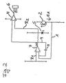
- FIG 2 is the circuit for stabilization according to the invention of the optical sensor.
- the one from the receiver outgoing line is connected to the negative pole of the amplifier, while at the positive pole the reference voltage lies.
- the difference between the reference voltage and the off The voltage derived from the receiver is through a resistor R3 returned to the LED.
- the LED has - as in the state of the Technology already exists - a ballast resistor R4, the Resistance value increased from 220 ohms to 1200 ohms has been. This ensures that the normal power supply the LED takes place via line 7 of the first amplifier.
- FIG. Figure 3a shows an encoder with a reflective layer, so that LED and photosensor arranged on one side of the clock disk are.
- the circuit according to the invention for stabilizing the Signals is in the base plate G1.
- Figure 3b is the encoder with a transparent clock disk shown. LED and photosensor are each on the opposite Arranged sides of the clock disc.
- the invention Circuit for the stabilization of the signal is located one in the base plate G2.
- the above-described process variant can be carried out by further Steps are added. So it is for the purpose of signal stabilization favorable if the output signal of the amplifier U7 via a memory unit to the negative input of the amplifier is returned.
- the storage unit can also preferably in the form of one or more capacitors connected in parallel available.
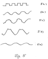
- Another alternative option is a Amplifier or transistor circuit in which the output of the first amplifier and the LED voltage on the plus-minus input of a second amplifier. By this way of switching is at the output of the second amplifier receive a sine curve in a rectangular shape (see FIG. 5a) above).
Landscapes
- Engineering & Computer Science (AREA)
- Power Engineering (AREA)
- Optical Transform (AREA)
- Photo Coupler, Interrupter, Optical-To-Optical Conversion Devices (AREA)
- Electronic Switches (AREA)
Abstract
Description
- Figur 1
- optischer Sensor nach dem Stand der Technik
- Figur 2
- erfindungsgemäßer Sensor mit LED feedback
- Figur 3
- erfindungsgemäß aufgebauter Encoder
- Figur 4
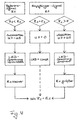
- bei einer erfindungsgemäßen Feed-Back-Schaltung Blockschaltbild für die Signalverarbeitung
- Figur 5
- verschiedene Kurvenverläufe bei der Signalstabilisierung
Claims (5)
- Verfahren zur Stabilisierung von optischen Signalen die von einer LED erzeugt und in einem Empfänger in eine Spannung umgewandelt werden,
dadurch gekennzeichnet, dass ein aus dem Empfänger abgeleitetes Spannungssignal in die Spannungsversorgung der LED zurückgeführt wird und dabei das Signal mit einer Referenzspannung verglichen wird, wobei bei einer Unterschreitung der Referenzspannung die LED-Eingangspannung erhöht und bei Überschreitung vermindert wird. - Verfahren nach Anspruch 1,
dadurch gekennzeichnet, dass der Vergleich in einem Differenzverstärker stattfindet. - Verfahren nach einem der vorhergehenden Ansprüche,
dadurch gekennzeichnet, dass in Stromflussrichtung hinter dem Differenzverstärker ein Vorschaltwiderstand angeordnet ist dessen Widerstandsbeiwert so bemessen ist, dass bei einer negativen Spannung keine zusätzliche Spannung in die LED-Spannungsquelle geleitet wird während bei einer positiven Spannungsdifferenz die LED-Spannungsquelle um den betreffenden positiven Spannungswert erhöht wird. - Verfahren zur Stabilisierung bei optischen Sensoren, die mit LED und einer Taktscheibe/ einem Taktlineal zu einer Sensor-Emittereinheit zusammengeschaltet sind,
dadurch gekennzeichnet, dass das Signal (E1) aus Empfänger (2) des Sensors vor Einleitung in den Eingang eines Verstärkers (3) mit einer Referenzspannung (R1) verglichen wird und daraus eine Differenzspannung (U7) gebildet wird, die über eine FeedbackLeitung(9) und über einen Speicher (8) an den Eingang des Verstärkers (3) zurückgeführt wird,
dass die Differenzspannung (U7) in einen zweiten Verstärker (4) eingegeben wird und dort mit einer zweiten Referenzspannung (R2) verglichen wird, die aus einer Addition der Differenzspannung (U7) mit einer Referenzspannung aus dem LED (5) erzeugt wird und dass das aus dem Vergleich mit der zweiten Referenzspannung (R2) resultierende Signal (6) des Verstärkers (4) als Kontrollsignal für die Stabilisierung des Sensorsignals verwendet wird. - Vorrichtung zur Signalstabilisierung bei optischen Sensoren, die mit einer LED (5) und einer Taktscheibe/ einem Taktlineal zu einer Sensor-Emittereinheit zusammengeschaltet sind,
dadurch gekennzeichnet, dass die Leitung (1) des Empfängers des Sensors (2) mit dem ersten Eingang eines Verstärkers (3) verbunden ist, dessen zweiter Eingang an einer Referenzquelle (R1) angeschlossen ist, wobei der Verstärkerausgang (7) einerseits über eine Feedbackleitung (9) und einen Kondensator (8) an den ersten Eingang des Verstärkers (3) zurückgeführt ist und andererseits in den ersten Eingang eines zweiten Verstärkers (4) angeschlossen ist, dessen zweiter Eingang mit einer Referenzspannungsquelle (R2) verbunden ist, und dass die Ausgangsleitung (6) des zweiten Verstärkers (4) an eine Kontrolleinheit für das stabilisierte Sensorsignal angeschlossen ist.
Applications Claiming Priority (2)
| Application Number | Priority Date | Filing Date | Title |
|---|---|---|---|
| DE10132540 | 2001-07-09 | ||
| DE10132540A DE10132540A1 (de) | 2001-07-09 | 2001-07-09 | Verfahren und Vorrichtung zur Signalstabilisierung |
Publications (4)
| Publication Number | Publication Date |
|---|---|
| EP1276228A2 true EP1276228A2 (de) | 2003-01-15 |
| EP1276228A8 EP1276228A8 (de) | 2004-03-31 |
| EP1276228A3 EP1276228A3 (de) | 2005-06-22 |
| EP1276228B1 EP1276228B1 (de) | 2009-01-21 |
Family
ID=7690668
Family Applications (1)
| Application Number | Title | Priority Date | Filing Date |
|---|---|---|---|
| EP02012791A Expired - Lifetime EP1276228B1 (de) | 2001-07-09 | 2002-06-10 | Verfahren und Vorrichtung zur Signalstabilisierung |
Country Status (7)
| Country | Link |
|---|---|
| US (1) | US20030006359A1 (de) |
| EP (1) | EP1276228B1 (de) |
| JP (1) | JP3802850B2 (de) |
| KR (1) | KR20030007051A (de) |
| DE (2) | DE10132540A1 (de) |
| HK (1) | HK1054630B (de) |
| TW (1) | TW583608B (de) |
Families Citing this family (3)
| Publication number | Priority date | Publication date | Assignee | Title |
|---|---|---|---|---|
| JP4508614B2 (ja) * | 2003-11-26 | 2010-07-21 | オリンパス株式会社 | 光学式エンコーダ |
| US20100007588A1 (en) * | 2008-07-09 | 2010-01-14 | Adaptive Micro Systems Llc | System and method for led degradation and temperature compensation |
| CN107631740A (zh) * | 2017-09-11 | 2018-01-26 | 珠海格力节能环保制冷技术研究中心有限公司 | 一种编码器光电补偿电路、方法及光电编码器 |
Family Cites Families (13)
| Publication number | Priority date | Publication date | Assignee | Title |
|---|---|---|---|---|
| CA1067597A (en) * | 1975-06-23 | 1979-12-04 | William J. Malinowski | Smoke detector |
| US4206456A (en) * | 1975-06-23 | 1980-06-03 | Chloride Incorporated | Smoke detector |
| JPS5681411A (en) * | 1979-12-08 | 1981-07-03 | Nippon Kogaku Kk <Nikon> | Detecting device for reference position |
| JPS5834367A (ja) * | 1981-08-25 | 1983-02-28 | Yokogawa Hokushin Electric Corp | 光応用測定器 |
| FI854809A7 (fi) * | 1984-12-18 | 1986-06-19 | Hochiki Co | Branddetektor som baserar sig pao minskat ljus. |
| JPS6327073A (ja) * | 1986-07-18 | 1988-02-04 | Fujikura Ltd | Led安定化光源 |
| JP2591608B2 (ja) * | 1986-08-13 | 1997-03-19 | 株式会社フジクラ | Led安定化光源 |
| JPH0710002B2 (ja) * | 1986-10-20 | 1995-02-01 | 株式会社フジクラ | Led安定化光源 |
| US5130556A (en) * | 1990-11-07 | 1992-07-14 | Eaton Corporation | Photoelectric fiber thickness and edge position sensor |
| JPH04256837A (ja) * | 1991-02-12 | 1992-09-11 | Ngk Spark Plug Co Ltd | 液体混合比センサの制御装置 |
| JPH08178618A (ja) * | 1994-12-21 | 1996-07-12 | Fujitsu Ten Ltd | 光学式センサ |
| US6350978B1 (en) * | 1999-02-18 | 2002-02-26 | Asahi Kogaku Kogyo Kabushiki Kaisha | Deterioration sensing device for light-emitting diode |
| US6344641B1 (en) * | 1999-08-11 | 2002-02-05 | Agilent Technologies, Inc. | System and method for on-chip calibration of illumination sources for an integrated circuit display |
-
2001
- 2001-07-09 DE DE10132540A patent/DE10132540A1/de not_active Withdrawn
-
2002
- 2002-06-10 DE DE50213229T patent/DE50213229D1/de not_active Expired - Fee Related
- 2002-06-10 EP EP02012791A patent/EP1276228B1/de not_active Expired - Lifetime
- 2002-07-08 US US10/191,259 patent/US20030006359A1/en not_active Abandoned
- 2002-07-08 KR KR1020020039314A patent/KR20030007051A/ko not_active Ceased
- 2002-07-09 TW TW091115375A patent/TW583608B/zh not_active IP Right Cessation
- 2002-07-09 JP JP2002199409A patent/JP3802850B2/ja not_active Expired - Fee Related
-
2003
- 2003-07-15 HK HK03105107.6A patent/HK1054630B/zh not_active IP Right Cessation
Also Published As
| Publication number | Publication date |
|---|---|
| EP1276228A3 (de) | 2005-06-22 |
| JP3802850B2 (ja) | 2006-07-26 |
| HK1054630B (zh) | 2009-10-02 |
| US20030006359A1 (en) | 2003-01-09 |
| HK1054630A1 (zh) | 2003-12-05 |
| KR20030007051A (ko) | 2003-01-23 |
| TW583608B (en) | 2004-04-11 |
| DE50213229D1 (de) | 2009-03-12 |
| EP1276228A8 (de) | 2004-03-31 |
| DE10132540A1 (de) | 2003-01-30 |
| EP1276228B1 (de) | 2009-01-21 |
| JP2003115603A (ja) | 2003-04-18 |
Similar Documents
| Publication | Publication Date | Title |
|---|---|---|
| DE3011052A1 (de) | Einbruchssicherungseinrichtung mit einer detektorleitung | |
| DE2461070C2 (de) | Akustische Prüfeinrichtung | |
| EP0366109A2 (de) | Verfahren und Vorrichtung zur Linearisierung des Frequenzganges eines Lautsprechersystems | |
| DE3536245A1 (de) | Vorrichtung zur messung der optischen dichte/des rasterpunkt-flaechenanteils | |
| DE2718491A1 (de) | Schaltungsanordnung zur verstaerkung der signale eines elektromagnetischen wandlers und zur vorspannungserzeugung fuer den wandler | |
| DE3804716A1 (de) | Vorrichtung zum messen der staerke von transportiertem blattmaterial | |
| EP0140091A2 (de) | Optoelektronischer Empfänger | |
| DE2720556C3 (de) | Schaltung zum Anzeigen der Impedanzanpassung eines Signalkopplungsnetzwerkes | |
| DE3333574C2 (de) | Datenextraktionsschaltung zur Wiedergewinnung von Daten von einem Aufzeichnungsmedium | |
| EP1276228A8 (de) | Verfahren und Vorrichtung zur Signalstabilisierung | |
| EP0032535A1 (de) | Vorrichtung zur opto-elektronischen Messung der Flächendeckung einer Offset-Druckplatte oder einer der Offset-Druckplattenherstellung dienenden Druckvorlage | |
| DE3010009C2 (de) | Oszillatorschaltung | |
| DE883923C (de) | Schaltungsanordnung zur Beseitigung bzw. Verringerung des Stoersignals | |
| DE3707100C2 (de) | ||
| DE2645705C3 (de) | Blutdruckmesser | |
| DE3234632C2 (de) | ||
| DE19750648C2 (de) | Induktivitätsänderungs-Erfassungsvorrichtung | |
| DE10005605B4 (de) | Analoge Vorstufe | |
| DE2130634B2 (de) | Anordnung zur Kompensation des Einflusses äußerer und/oder innerer Störgrößen auf das Ausgangssignal eines Meßorgans | |
| DE4134578C2 (de) | Schaltungsanordnung zur Erzeugung von Audiosignalen Klang-/Toneffekte erteilenden Oberwellen | |
| EP0774651A2 (de) | Differenzdrucksensor | |
| AT269219B (de) | Linear-veränderlicher Sinusoszillator | |
| DE19629488C2 (de) | Vorrichtung zum Gewinnen von oberwellenfreien Signalen | |
| DE3536590A1 (de) | Klangreglerschaltkreis mit gegenkopplung | |
| DE3236178C2 (de) | Kanal-Regelverstärker für den UHF- oder VHF-Bereich in einer Fernseh-Empfangsanlage |
Legal Events
| Date | Code | Title | Description |
|---|---|---|---|
| PUAI | Public reference made under article 153(3) epc to a published international application that has entered the european phase |
Free format text: ORIGINAL CODE: 0009012 |
|
| AK | Designated contracting states |
Kind code of ref document: A2 Designated state(s): AT BE CH CY DE DK ES FI FR GB GR IE IT LI LU MC NL PT SE TR |
|
| AX | Request for extension of the european patent |
Free format text: AL;LT;LV;MK;RO;SI |
|
| 17P | Request for examination filed |
Effective date: 20030702 |
|
| RIN1 | Information on inventor provided before grant (corrected) |
Inventor name: BARI, ANDREA Inventor name: TENCA, VITTORIO Inventor name: CARRADORI, CORRADO Inventor name: ZANOTTI, ERNESTO |
|
| PUAL | Search report despatched |
Free format text: ORIGINAL CODE: 0009013 |
|
| AK | Designated contracting states |
Kind code of ref document: A3 Designated state(s): AT BE CH CY DE DK ES FI FR GB GR IE IT LI LU MC NL PT SE TR |
|
| AX | Request for extension of the european patent |
Extension state: AL LT LV MK RO SI |
|
| RIC1 | Information provided on ipc code assigned before grant |
Ipc: 7H 03F 3/08 A Ipc: 7G 01R 15/22 B Ipc: 7G 01D 5/34 B |
|
| AKX | Designation fees paid |
Designated state(s): CH DE FR GB IT LI |
|
| GRAP | Despatch of communication of intention to grant a patent |
Free format text: ORIGINAL CODE: EPIDOSNIGR1 |
|
| GRAS | Grant fee paid |
Free format text: ORIGINAL CODE: EPIDOSNIGR3 |
|
| GRAA | (expected) grant |
Free format text: ORIGINAL CODE: 0009210 |
|
| AK | Designated contracting states |
Kind code of ref document: B1 Designated state(s): CH DE FR GB IT LI |
|
| REG | Reference to a national code |
Ref country code: GB Ref legal event code: FG4D Free format text: NOT ENGLISH |
|
| REG | Reference to a national code |
Ref country code: CH Ref legal event code: EP |
|
| REF | Corresponds to: |
Ref document number: 50213229 Country of ref document: DE Date of ref document: 20090312 Kind code of ref document: P |
|
| REG | Reference to a national code |
Ref country code: HK Ref legal event code: GR Ref document number: 1054630 Country of ref document: HK |
|
| PLBE | No opposition filed within time limit |
Free format text: ORIGINAL CODE: 0009261 |
|
| STAA | Information on the status of an ep patent application or granted ep patent |
Free format text: STATUS: NO OPPOSITION FILED WITHIN TIME LIMIT |
|
| 26N | No opposition filed |
Effective date: 20091022 |
|
| REG | Reference to a national code |
Ref country code: CH Ref legal event code: PL |
|
| GBPC | Gb: european patent ceased through non-payment of renewal fee |
Effective date: 20090610 |
|
| REG | Reference to a national code |
Ref country code: FR Ref legal event code: ST Effective date: 20100226 |
|
| PG25 | Lapsed in a contracting state [announced via postgrant information from national office to epo] |
Ref country code: CH Free format text: LAPSE BECAUSE OF NON-PAYMENT OF DUE FEES Effective date: 20090630 Ref country code: FR Free format text: LAPSE BECAUSE OF NON-PAYMENT OF DUE FEES Effective date: 20090630 Ref country code: LI Free format text: LAPSE BECAUSE OF NON-PAYMENT OF DUE FEES Effective date: 20090630 |
|
| PG25 | Lapsed in a contracting state [announced via postgrant information from national office to epo] |
Ref country code: GB Free format text: LAPSE BECAUSE OF NON-PAYMENT OF DUE FEES Effective date: 20090610 |
|
| PG25 | Lapsed in a contracting state [announced via postgrant information from national office to epo] |
Ref country code: DE Free format text: LAPSE BECAUSE OF NON-PAYMENT OF DUE FEES Effective date: 20100101 |
|
| PG25 | Lapsed in a contracting state [announced via postgrant information from national office to epo] |
Ref country code: IT Free format text: LAPSE BECAUSE OF NON-PAYMENT OF DUE FEES Effective date: 20090610 |