EP1276142A2 - Verfahren und Apparat zum Entkapseln von integrierten Schaltungspackungen - Google Patents
Verfahren und Apparat zum Entkapseln von integrierten Schaltungspackungen Download PDFInfo
- Publication number
- EP1276142A2 EP1276142A2 EP01309771A EP01309771A EP1276142A2 EP 1276142 A2 EP1276142 A2 EP 1276142A2 EP 01309771 A EP01309771 A EP 01309771A EP 01309771 A EP01309771 A EP 01309771A EP 1276142 A2 EP1276142 A2 EP 1276142A2
- Authority
- EP
- European Patent Office
- Prior art keywords
- decapping
- package
- laser
- complete
- integrated circuit
- Prior art date
- Legal status (The legal status is an assumption and is not a legal conclusion. Google has not performed a legal analysis and makes no representation as to the accuracy of the status listed.)
- Withdrawn
Links
Images


Classifications
-
- H10W72/071—
-
- B—PERFORMING OPERATIONS; TRANSPORTING
- B23—MACHINE TOOLS; METAL-WORKING NOT OTHERWISE PROVIDED FOR
- B23K—SOLDERING OR UNSOLDERING; WELDING; CLADDING OR PLATING BY SOLDERING OR WELDING; CUTTING BY APPLYING HEAT LOCALLY, e.g. FLAME CUTTING; WORKING BY LASER BEAM
- B23K26/00—Working by laser beam, e.g. welding, cutting or boring
- B23K26/36—Removing material
- B23K26/361—Removing material for deburring or mechanical trimming
-
- H10W72/0711—
-
- H10W74/01—
-
- B—PERFORMING OPERATIONS; TRANSPORTING
- B23—MACHINE TOOLS; METAL-WORKING NOT OTHERWISE PROVIDED FOR
- B23K—SOLDERING OR UNSOLDERING; WELDING; CLADDING OR PLATING BY SOLDERING OR WELDING; CUTTING BY APPLYING HEAT LOCALLY, e.g. FLAME CUTTING; WORKING BY LASER BEAM
- B23K2101/00—Articles made by soldering, welding or cutting
- B23K2101/36—Electric or electronic devices
- B23K2101/40—Semiconductor devices
-
- B—PERFORMING OPERATIONS; TRANSPORTING
- B23—MACHINE TOOLS; METAL-WORKING NOT OTHERWISE PROVIDED FOR
- B23K—SOLDERING OR UNSOLDERING; WELDING; CLADDING OR PLATING BY SOLDERING OR WELDING; CUTTING BY APPLYING HEAT LOCALLY, e.g. FLAME CUTTING; WORKING BY LASER BEAM
- B23K2103/00—Materials to be soldered, welded or cut
- B23K2103/30—Organic material
- B23K2103/42—Plastics
-
- B—PERFORMING OPERATIONS; TRANSPORTING
- B23—MACHINE TOOLS; METAL-WORKING NOT OTHERWISE PROVIDED FOR
- B23K—SOLDERING OR UNSOLDERING; WELDING; CLADDING OR PLATING BY SOLDERING OR WELDING; CUTTING BY APPLYING HEAT LOCALLY, e.g. FLAME CUTTING; WORKING BY LASER BEAM
- B23K2103/00—Materials to be soldered, welded or cut
- B23K2103/50—Inorganic material, e.g. metals, not provided for in B23K2103/02 – B23K2103/26
-
- H—ELECTRICITY
- H01—ELECTRIC ELEMENTS
- H01L—SEMICONDUCTOR DEVICES NOT COVERED BY CLASS H10
- H01L2224/00—Indexing scheme for arrangements for connecting or disconnecting semiconductor or solid-state bodies and methods related thereto as covered by H01L24/00
- H01L2224/01—Means for bonding being attached to, or being formed on, the surface to be connected, e.g. chip-to-package, die-attach, "first-level" interconnects; Manufacturing methods related thereto
- H01L2224/42—Wire connectors; Manufacturing methods related thereto
- H01L2224/44—Structure, shape, material or disposition of the wire connectors prior to the connecting process
- H01L2224/45—Structure, shape, material or disposition of the wire connectors prior to the connecting process of an individual wire connector
- H01L2224/45001—Core members of the connector
- H01L2224/45099—Material
- H01L2224/451—Material with a principal constituent of the material being a metal or a metalloid, e.g. boron (B), silicon (Si), germanium (Ge), arsenic (As), antimony (Sb), tellurium (Te) and polonium (Po), and alloys thereof
- H01L2224/45138—Material with a principal constituent of the material being a metal or a metalloid, e.g. boron (B), silicon (Si), germanium (Ge), arsenic (As), antimony (Sb), tellurium (Te) and polonium (Po), and alloys thereof the principal constituent melting at a temperature of greater than or equal to 950°C and less than 1550°C
- H01L2224/45147—Copper (Cu) as principal constituent
-
- H10W72/01515—
-
- H10W72/075—
-
- H10W72/5522—
-
- H10W72/5525—
-
- H10W74/00—
-
- H10W74/10—
-
- H10W90/756—
Definitions
- the invention relates to the field of decapping integrated circuits (also known as decapsulating or unpacking), particularly in preparation for device failure analysis.
- the invention relates to a method and apparatus for decapping IC packages.
- Integrated circuit (IC) packaging typically involves placing a small wafer die on a leadframe (commonly a copper leadframe). Tiny copper or gold lines are then soldered to the corresponding lead legs in the leadframe and bond pads on the wafer die so as to provide electrical connections. In order to protect the device from environmental factors such as heat and humidity, a thin transparent layer of epoxy materials is typically then bonded to the upper surface of the wafer die, completely covering the die. The assembly is then encapsulated using a molding compound (usually black), so as to provide an IC package.
- a molding compound usually black
- IC package failure analysis An important area of study in the IC industry is that of IC package failure analysis, which is vital in helping manufacturers to understand and address the causes of device failure whereby to improve manufacturing yield and device reliability.
- One technique is that of electric signal detection, diagnosis of the results of which can give some insights into the reasons for device failure.
- diagnosis of the results of which can give some insights into the reasons for device failure.
- using this technique it is difficult to obtain enough information for complete analysis, particularly as circuits become more and more integrated.
- a more thorough method of device failure analysis involves unpacking the IC package by removing the black molding compounds covering the wafer die and epoxy layer. This is known as decapping or decapsulating an IC package.
- One decapping technique widely used is that of chemical decapping.
- chemical decapping sulfuric and/or nitric acide are used, depending on the molding compound(s) to be removed. Chemical decapping can take several hours and can potentially damage bond pads, solder balls and copper traces in the organic die attachments, in addition to damaging the leadframe itself. It can therefore be complicated and difficult to achieve thorough decapping while avoiding such collateral damage.
- the invention provides a method for decapping an integrated circuit package , the said package comprising one or more layers of electronic circuitry covered by one or more layers of capping material, characterised in that the method includes the step of irradiating the integrated circuit package with laser radiation so as to remove the said capping material.
- the method includes the step of selecting a selected location on the package to be irradiated before performing the irradiation step.
- the method further includes the steps of monitoring the decapping process; determining whether decapping is complete at the said selected location; if the above determination is negative, continuing to irradiate the package and if the above determination is positive, determining whether all decapping is complete; if all decapping has been determined to be complete, stopping the decapping process, and if all decapping has not been determined to be complete, selecting a new location at which the laser energy is to be directed and continuing to irradiate the package.
- the said determination as to whether decapping is complete at the said location involves the monitoring of acoustic and/or optical signals emanating from the decapping location.
- the method includes the steps of measuring the energy of the laser radiation; comparing the measured energy of the laser radiation with an expected value and adjusting the laser energy accordingly if the two values do not correspond.
- a fluid preferably a liquid (e.g. water or Isopropyl Alcohol solution), is caused to flow over the package.
- the package is preferably immersed in liquid during the decapping process.
- the fluid may alternatively be a gas, e.g. air.
- the invention may comprise a device suitable for carrying out the above method.
- FIGS 1a and 1b show a cross-sectional slice through an IC package before and after decapping according to the invention.
- an IC package (1) comprises a leadframe (2) upon which sits a wafer die (3).
- Wires, typically gold wires (4) form electrical connections between the leadframe (2) and wafer die (3).
- Covering the wafer die is a layer of transparent epoxy material (5).
- the wafer die and associated electrical connections are encapsulated by a layer of (usually black) molding material (6).
- Figure 1b shows the same view of the package after decapping.
- the layer of molding material (1) covering the wafer die (3) has been removed so that the upper surface of the wafer die (which bears electrical circuitry (not shown)) can be examined through the transparent epoxy layer (5).
- the connections between the wires (4) and wafer die (3) can also be examined. If more molding material is removed by further decapping, the connections between the wires (4) and leadframe (2) can also be examined.
- FIG. 2 shows apparatus suitable for carrying out the present invention.
- the figure shows a laser light source (7), preferably having a short pulse duration and wavelength in the UV to IR spectra.
- a suitable laser is for example a Nd:YAG laser having a pulse duration of 7 ns and a wavelength of 532 nm.
- the laser source (7) emits a beam (8), which then passes through a beam sampler (9).
- the beam sampler (9) passes a small percentage (e.g. 5%) of the beam to an energy meter (10), which monitors the laser pulse energy in real time.
- the reading of the meter (10) is sent to a process controller (11).
- the process controller compares the actual value with the expected value and if the two values do not coincide, adjusts the laser source output accordingly.
- the rest of the beam (8) passes to a beam expander (12) which produces an expanded beam (13).
- This expanded beam is reflected by a mirror (14) into a beam homogenizer (15) which produces a homogenized beam (16), which passes through an aperture (17) before being incident on the IC package (1).
- the homogenized beam provides a uniform energy profile on the package, the spot size of the beam on the package being controllable by the aperture (17).
- the IC package (1) is held inside a decapping chamber (18).
- the decapping chamber (18) is coupled with a gas stream or suction system to remove the ablation debris.
- the decapping chamber contains a liquid (19) (e.g. water, Isopropyl Alcohol (IPA) solution or other suitable liquid) in which the package is immersed.
- the liquid prevents oxidation of the molding compound, thereby speeding up the process and necessitating a lower laser fluence.
- a liquid inlet (20) and outlet (21) are provided and a flow of liquid is maintained. Ablation debris is entrained in the flow of liquid and evacuated from the chamber via the liquid outlet (21).
- the decapping chamber (18) is held on an X-Y stage (22), the movement of which is controlled by the process controller (10) in order to effect relative displacement of the laser and package surface so that the laser beam may be scanned over the package surface as desired.
- the laser beam itself may be moved over the surface.
- a CCD camera (23) and associated monitor (24) are used to provide an image of the progress of the decapping process. Furthermore, during laser ablation of molding compounds, acoustic and optical signals are generated. The signal amplitude gives a measure of progress of the ablation process.
- An acoustic and/or optical monitoring device (25) may therefore be used in conjunction with the process controller (10) to monitor the ablation process in real time and to provide feedback control to the apparatus.
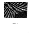
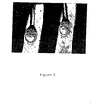
- Figures 3 - 7 are microphotographs of various areas of a package which has been decapped according to the invention.
- Figure 3 shows a decapped leadframe
- Figure 4 decapped wires
- Figure 5 shows decapped solder bonds to the leadframe
- Figure 6 shows decapped bond pads of a wafer die
- Figure 7 shows the circuit configuration on a wafer die. As can be seen, decapping has been achieved without damaging the package structure.
- Figure 8 is a flowchart illustrating the method of the invention.
- the package to be decapped is placed (27) in the decapping chamber.
- the package is moved (28) to its decapping position so as to be in the path of the laser beam.
- the flow of fluid over the package is initiated (29).
- the location to be irradiated is selected (30).
- the package is irradiated (31).
- the laser energy is measured (32) and it is determined (33) whether the actual value differs from the expected value. If so, the laser energy is adjusted (34). If the laser energy is as expected, the acoustic/optical signals emanating from the decapping region are monitored (35).
- decapping continues (31). If decapping is complete at this location, a further determination is made as to whether or not all decapping is complete (37). If so, the process ends (38). If not, a new location to be irradiated is selected (39) and decapping continues (31) at a new location.
- the method of the invention is a non-contact process, which allows the unpacking of the wafer die of an IC package for device failure analysis. Careful selection of laser processing parameters, such as pulse repetition rate, laser fluence, laser wavelength and pulse duration is required in order to achieve efficient and rapid laser decapping without compromising the internal IC package structure. No decapping chemicals are required and no chemical reactions take place on the epoxy layer, metal or semiconductor structures.
- Molding compound is easily ablated using pulsed laser irradiation. Its ablation threshold fluence is much lower than those of metal /semiconductor materials.
- the fluid can be a gas, e.g. air, or a fluid, e.g. water or Isopropyl Alcohol (IPA) solution.
- Laser ablation is preferably carried out inside a liquid, the package being completely immersed. This will increase the ablation speed substantially as the oxidation of molding compounds due to ambient air can be prevented. Oxidation may also be prevented by performing the decapping in an inert atmosphere.
- the use of fluid immersion requires lower laser fluence.
- the laser fluence is a critical parameter. Too high a laser fluence, although increasing the processing speed, may result in damage to the epoxy layer, metal and/or semiconductor structures, especially at the interface with the molding compound. Since, as discussed, the ablation threshold of the molding compound is lower than that of the other materials, it is possible to select a value for the laser fluence which will not cause such collateral damage. The technique therefore has significant advantages over chemical decapping.
- the invention relates to a method and apparatus for decapping integrated circuit packages.
- the invention involves irradiating an IC package with laser radiation, typically in the UV - IR spectra and of short pulse duration. The irradiation results in ablation of the molding compound.
- the invention also provides real-time monitoring and process control of the decapping process and fluid-flow removal of ablation debris. Using the invention, decapping can be performed without causing damage to the internal IC structure. Furthermore, decapping in a liquid can prevent oxidisation of the molding compound by ambient air.
Landscapes
- Engineering & Computer Science (AREA)
- Physics & Mathematics (AREA)
- Optics & Photonics (AREA)
- Plasma & Fusion (AREA)
- Mechanical Engineering (AREA)
- Encapsulation Of And Coatings For Semiconductor Or Solid State Devices (AREA)
- Laser Beam Processing (AREA)
- Testing Or Measuring Of Semiconductors Or The Like (AREA)
- Wire Bonding (AREA)
Applications Claiming Priority (2)
| Application Number | Priority Date | Filing Date | Title |
|---|---|---|---|
| SG200104149 | 2001-07-11 | ||
| SG200104149A SG111023A1 (en) | 2001-07-11 | 2001-07-11 | Method and apparatus for decapping integrated circuit packages |
Publications (2)
| Publication Number | Publication Date |
|---|---|
| EP1276142A2 true EP1276142A2 (de) | 2003-01-15 |
| EP1276142A3 EP1276142A3 (de) | 2005-06-01 |
Family
ID=20430803
Family Applications (1)
| Application Number | Title | Priority Date | Filing Date |
|---|---|---|---|
| EP01309771A Withdrawn EP1276142A3 (de) | 2001-07-11 | 2001-11-21 | Verfahren und Apparat zum Entkapseln von integrierten Schaltungspackungen |
Country Status (5)
| Country | Link |
|---|---|
| US (1) | US6917011B2 (de) |
| EP (1) | EP1276142A3 (de) |
| JP (1) | JP2003045921A (de) |
| SG (1) | SG111023A1 (de) |
| TW (1) | TWI253151B (de) |
Cited By (9)
| Publication number | Priority date | Publication date | Assignee | Title |
|---|---|---|---|---|
| WO2005010945A2 (en) | 2003-07-15 | 2005-02-03 | Control Systemation, Inc. | Failure analysis methods and systems |
| EP2073262A1 (de) * | 2007-12-18 | 2009-06-24 | Micronas GmbH | Halbleiterbauelement |
| WO2009081243A1 (en) * | 2007-12-21 | 2009-07-02 | Schlumberger Technology B.V. | Downhole tool |
| US8842951B2 (en) | 2012-03-02 | 2014-09-23 | Analog Devices, Inc. | Systems and methods for passive alignment of opto-electronic components |
| US9590129B2 (en) | 2014-11-19 | 2017-03-07 | Analog Devices Global | Optical sensor module |
| US9716193B2 (en) | 2012-05-02 | 2017-07-25 | Analog Devices, Inc. | Integrated optical sensor module |
| CN108956615A (zh) * | 2018-05-09 | 2018-12-07 | 苏州康鸿智能装备股份有限公司 | 一种电子产品外壳激光表面修复工艺 |
| US10712197B2 (en) | 2018-01-11 | 2020-07-14 | Analog Devices Global Unlimited Company | Optical sensor package |
| US10884551B2 (en) | 2013-05-16 | 2021-01-05 | Analog Devices, Inc. | Integrated gesture sensor module |
Families Citing this family (17)
| Publication number | Priority date | Publication date | Assignee | Title |
|---|---|---|---|---|
| US6335208B1 (en) | 1999-05-10 | 2002-01-01 | Intersil Americas Inc. | Laser decapsulation method |
| US20020170897A1 (en) * | 2001-05-21 | 2002-11-21 | Hall Frank L. | Methods for preparing ball grid array substrates via use of a laser |
| WO2007005636A2 (en) * | 2005-06-30 | 2007-01-11 | Controlled Semiconductor, Inc. | Semiconductor failure analysis tool |
| US7279343B1 (en) * | 2005-07-25 | 2007-10-09 | National Semiconductor Corporation | De-packaging process for small outline transistor packages |
| US7937936B2 (en) * | 2007-01-16 | 2011-05-10 | Deere & Company | Vehicle exhaust component arrangement |
| TW200917431A (en) | 2007-10-05 | 2009-04-16 | Advanced Semiconductor Eng | Stacked-type chip package structure and method of fabricating the same |
| TW200936287A (en) * | 2007-11-26 | 2009-09-01 | Nat Inst Of Advanced Ind Scien | Mold removing method |
| JP5224139B2 (ja) * | 2009-10-27 | 2013-07-03 | 独立行政法人産業技術総合研究所 | モールド除去方法およびモールド除去装置 |
| US8197037B2 (en) * | 2009-12-15 | 2012-06-12 | Xerox Corporation | Method of removing thermoset polymer from piezoelectric transducers in a print head |
| JP5435016B2 (ja) * | 2011-12-01 | 2014-03-05 | 株式会社デンソー | 半導体装置の製造方法 |
| CN102601522B (zh) * | 2012-03-30 | 2014-05-28 | 天津大学 | 飞秒激光辅助超临界流体进行高分子材料微加工方法 |
| JP5928379B2 (ja) * | 2013-03-19 | 2016-06-01 | 株式会社デンソー | 半導体装置の製造方法 |
| RU169247U1 (ru) * | 2016-08-23 | 2017-03-13 | Закрытое акционерное общество "ГРУППА КРЕМНИЙ ЭЛ" | Устройство для вскрытия пластиковых корпусов полупроводниковых приборов и микросхем лазером |
| CN106271057B (zh) * | 2016-09-28 | 2018-03-09 | 西安交通大学 | 一种基于空气及水环境的时序激光打孔装置及方法 |
| US20210107094A1 (en) * | 2019-10-14 | 2021-04-15 | Haesung Ds Co., Ltd. | Apparatus for and method of polishing surface of substrate |
| JP2022021071A (ja) * | 2020-07-21 | 2022-02-02 | 日本サイエンティフィック株式会社 | 半導体装置パッケージの開封方法及び半導体装置パッケージの開封装置 |
| CN116013817B (zh) * | 2023-01-17 | 2024-03-19 | 上海季丰电子股份有限公司 | 芯片封装破除装置及方法 |
Family Cites Families (13)
| Publication number | Priority date | Publication date | Assignee | Title |
|---|---|---|---|---|
| GB2156742B (en) * | 1984-04-06 | 1987-01-28 | Standard Telephones Cables Ltd | Etching plastics encapsulated electronic packages |
| JPS6172030A (ja) * | 1984-09-18 | 1986-04-14 | Mitsubishi Electric Corp | 電子部品の樹脂溶解加速方法 |
| US5350713A (en) * | 1990-12-19 | 1994-09-27 | Vlsi Technology, Inc. | Design and sealing method for semiconductor packages |
| JP2707189B2 (ja) * | 1992-08-26 | 1998-01-28 | 株式会社日立製作所 | 電子部品の基板からの取外し方法及び装置 |
| US5367762A (en) * | 1992-12-23 | 1994-11-29 | Advanced Micro Devices, Inc. | Decapping machine for packaged integrated circuits |
| US5976955A (en) * | 1995-01-04 | 1999-11-02 | Micron Technology, Inc. | Packaging for bare dice employing EMR-sensitive adhesives |
| US5961860A (en) * | 1995-06-01 | 1999-10-05 | National University Of Singapore | Pulse laser induced removal of mold flash on integrated circuit packages |
| JP3132453B2 (ja) * | 1998-02-20 | 2001-02-05 | 日本電気株式会社 | モールド樹脂のエッチング方法及びそのエッチング装置 |
| US6054012A (en) * | 1998-06-29 | 2000-04-25 | Intersil Corporation | Decapsulating method and apparatus for integrated circuit packages |
| US6335208B1 (en) * | 1999-05-10 | 2002-01-01 | Intersil Americas Inc. | Laser decapsulation method |
| US6277659B1 (en) * | 1999-09-29 | 2001-08-21 | Advanced Micro Devices, Inc. | Substrate removal using thermal analysis |
| CA2356253C (en) | 1999-10-29 | 2010-10-26 | Kawasaki Steel Corporation | A die lubricant comprising a higher-melting and a lower-melting lubricants |
| US6518074B1 (en) * | 2000-09-28 | 2003-02-11 | National Semiconductor Corporation | Backside IC device preparation process |
-
2001
- 2001-07-11 SG SG200104149A patent/SG111023A1/en unknown
- 2001-09-04 TW TW090121898A patent/TWI253151B/zh not_active IP Right Cessation
- 2001-11-21 EP EP01309771A patent/EP1276142A3/de not_active Withdrawn
- 2001-11-26 JP JP2001359448A patent/JP2003045921A/ja active Pending
-
2002
- 2002-07-10 US US10/193,773 patent/US6917011B2/en not_active Expired - Fee Related
Cited By (12)
| Publication number | Priority date | Publication date | Assignee | Title |
|---|---|---|---|---|
| WO2005010945A2 (en) | 2003-07-15 | 2005-02-03 | Control Systemation, Inc. | Failure analysis methods and systems |
| EP1652221A4 (de) * | 2003-07-15 | 2007-10-17 | Control Systemation Inc | Ausfallanalyseverfahren und systeme |
| EP2073262A1 (de) * | 2007-12-18 | 2009-06-24 | Micronas GmbH | Halbleiterbauelement |
| US8125070B2 (en) | 2007-12-18 | 2012-02-28 | Micronas Gmbh | Semiconductor component |
| WO2009081243A1 (en) * | 2007-12-21 | 2009-07-02 | Schlumberger Technology B.V. | Downhole tool |
| US8842951B2 (en) | 2012-03-02 | 2014-09-23 | Analog Devices, Inc. | Systems and methods for passive alignment of opto-electronic components |
| US9348088B2 (en) | 2012-03-02 | 2016-05-24 | Analog Devices, Inc. | Systems and methods for passive alignment of opto-electronic components |
| US9716193B2 (en) | 2012-05-02 | 2017-07-25 | Analog Devices, Inc. | Integrated optical sensor module |
| US10884551B2 (en) | 2013-05-16 | 2021-01-05 | Analog Devices, Inc. | Integrated gesture sensor module |
| US9590129B2 (en) | 2014-11-19 | 2017-03-07 | Analog Devices Global | Optical sensor module |
| US10712197B2 (en) | 2018-01-11 | 2020-07-14 | Analog Devices Global Unlimited Company | Optical sensor package |
| CN108956615A (zh) * | 2018-05-09 | 2018-12-07 | 苏州康鸿智能装备股份有限公司 | 一种电子产品外壳激光表面修复工艺 |
Also Published As
| Publication number | Publication date |
|---|---|
| US20030010761A1 (en) | 2003-01-16 |
| EP1276142A3 (de) | 2005-06-01 |
| TWI253151B (en) | 2006-04-11 |
| JP2003045921A (ja) | 2003-02-14 |
| SG111023A1 (en) | 2005-05-30 |
| US6917011B2 (en) | 2005-07-12 |
Similar Documents
| Publication | Publication Date | Title |
|---|---|---|
| US6917011B2 (en) | Method and apparatus for decapping integrated circuit packages | |
| US7705267B2 (en) | Semiconductor failure analysis tool | |
| US7271012B2 (en) | Failure analysis methods and systems | |
| USRE43980E1 (en) | Laser decapsulation method | |
| US6781093B2 (en) | Circuit singulation system and method | |
| US7170029B2 (en) | Method and apparatus for deflashing of integrated circuit packages | |
| US20060163573A1 (en) | Method for preparing ball grid array substrates via use of a laser | |
| US20050184133A1 (en) | Laser cleaning system for a wire bonding machine | |
| KR20090124928A (ko) | 웨이퍼 분할 방법 | |
| KR102238569B1 (ko) | 레이저 가공 장치 및 웨이퍼의 생성 방법 | |
| US20220023975A1 (en) | Unsealing method of semiconductor device package and unsealing device of semiconductor device package | |
| CN113871313A (zh) | 芯片的检测系统及检测方法 | |
| NL1018403C1 (nl) | Werkwijze voor het onder toepassing van een laser snijden van een composietstructuur met een of meer elektronische componenten. | |
| NL2008943C2 (en) | Plasma jet etching device and method for removing an encapsulation portion of a sample via plasma jet etching. | |
| CN113878253A (zh) | 晶片的检查方法 | |
| CN113909697A (zh) | 激光开封系统及激光开封方法 | |
| Hecht et al. | Laser cleaning of flux residues on copper surfaces in electronics production | |
| Spletter et al. | A laser based system for tape automated bonding to integrated circuits | |
| KR101814493B1 (ko) | 반도체 몰딩수지 선택 제거 장치 및 방법 | |
| Hong et al. | Pulsed laser ablation of IC packages for device failure analyses | |
| Kor et al. | Hardware Security Evaluation of Advanced Packaging | |
| Klengel et al. | A New, Efficient Method for Preparation of 3D Integrated Systems by Laser Techniques | |
| Song et al. | Laser-induced removal of flash from heat sinks in integrated circuit packages | |
| JPH07311181A (ja) | 音波を用いた基板表面状態検出方法およびその装置 | |
| Harvilchuck et al. | Laser ablation of anisotropic conductive adhesive |
Legal Events
| Date | Code | Title | Description |
|---|---|---|---|
| PUAI | Public reference made under article 153(3) epc to a published international application that has entered the european phase |
Free format text: ORIGINAL CODE: 0009012 |
|
| AK | Designated contracting states |
Kind code of ref document: A2 Designated state(s): AT BE CH CY DE DK ES FI FR GB GR IE IT LI LU MC NL PT SE TR |
|
| AX | Request for extension of the european patent |
Free format text: AL;LT;LV;MK;RO;SI |
|
| PUAL | Search report despatched |
Free format text: ORIGINAL CODE: 0009013 |
|
| AK | Designated contracting states |
Kind code of ref document: A3 Designated state(s): AT BE CH CY DE DK ES FI FR GB GR IE IT LI LU MC NL PT SE TR |
|
| AX | Request for extension of the european patent |
Extension state: AL LT LV MK RO SI |
|
| STAA | Information on the status of an ep patent application or granted ep patent |
Free format text: STATUS: THE APPLICATION IS DEEMED TO BE WITHDRAWN |
|
| 18D | Application deemed to be withdrawn |
Effective date: 20050202 |