EP1271183A2 - Optoelektronischer Sensor - Google Patents
Optoelektronischer Sensor Download PDFInfo
- Publication number
- EP1271183A2 EP1271183A2 EP02011871A EP02011871A EP1271183A2 EP 1271183 A2 EP1271183 A2 EP 1271183A2 EP 02011871 A EP02011871 A EP 02011871A EP 02011871 A EP02011871 A EP 02011871A EP 1271183 A2 EP1271183 A2 EP 1271183A2
- Authority
- EP
- European Patent Office
- Prior art keywords
- sum
- threshold value
- difference
- received signals
- detection signal
- Prior art date
- Legal status (The legal status is an assumption and is not a legal conclusion. Google has not performed a legal analysis and makes no representation as to the accuracy of the status listed.)
- Granted
Links
Images




Classifications
-
- G—PHYSICS
- G01—MEASURING; TESTING
- G01V—GEOPHYSICS; GRAVITATIONAL MEASUREMENTS; DETECTING MASSES OR OBJECTS; TAGS
- G01V8/00—Prospecting or detecting by optical means
- G01V8/10—Detecting, e.g. by using light barriers
- G01V8/12—Detecting, e.g. by using light barriers using one transmitter and one receiver
Definitions
- the invention relates to an optoelectronic sensor, in particular a reflection light scanner, at least with a transmitter for emitting transmission light, a receiver for outputting at least two received signals depending on reflected and received transmission light, and an evaluation device through which to determine whether a Object or no object is in a detection range of the sensor, a difference in the received signals with a threshold value comparable is positive and depending on the result of this comparison or negative object detection signal can be generated, wherein for Generation of a switching hysteresis of several different threshold values are provided.
- the invention further relates to a corresponding method.
- Such sensors are intended to detect whether and when an object is in the detection area arrives or leaves it, whereas objects in others Areas should be ignored.
- background suppression in the detection area act as a foreground area; if an object from the The sensor should change the foreground area to the background area from a positive to a negative object detection signal switch.
- Such sensors usually work according to the triangulation principle: A change in the distance of a reflecting object (scanning distance) leads to a shift of the corresponding light spot the receiver and a corresponding change in the output signals the receiver or the differential signal of a downstream differential circuit. If this difference signal is due to such a change exceeds or falls below a difference threshold, switches Evaluation unit for a positive or negative object detection signal around.
- the threshold value therefore corresponds to a certain one Operating distance.
- a Switching hysteresis should be provided: As soon as the sensor switches from positive to switches the negative object detection signal - or vice versa - is also used as the basis for the further comparison of the difference signal Threshold value changed so that the difference signal now make a sufficiently clear change in the opposite direction needs to change the item detection signal again bring about.
- This task is achieved for a sensor of the type mentioned solved that the evaluation device is designed such that as an additional Criterion for the generation of the object detection signal the result of a comparison of a sum of the received signals is provided with a threshold.
- the task becomes an appropriate detection method solved that as an additional criterion for the generation of the object detection signal a sum of the received signals with a Threshold is compared.
- a difference signal takes another condition into account:
- the sum of the received signals is also determined and by means of a comparison device with one or more threshold values (Sum threshold values) compared.
- the invention is based on the knowledge that the respective path hysteresis least for objects with different reflectivities distinguishes if the difference thresholds the distance correspond for which the two received signals are the same size, that is, for the difference in the received signals is zero.
- Differential threshold values cannot, however, in the known sensors be realized because at a difference threshold that is within the RMS value (Root Mean Square) of the noise of the difference signal or even below zero, is no longer guaranteed, that a negative object detection signal is generated when the Sensor sees no object (so-called look into the void).
- This possible source of error is in the invention by the additional Comparison of the sum signal with a sum threshold avoided.
- the sum comparison makes false detections that occur at Setting the differential threshold values close to zero occur can prevented.
- the difference threshold values can thus be chosen freely to reduce the variation in path hysteresis can.
- the output signal of one of the at least two received signals processing differential circuit or sum circuit, or the input signal to understand a downstream comparison device.
- the switching hysteresis it is preferred if both for the Difference comparison as well as two threshold values for the sum comparison selected and - depending on the switching direction - taken into account.
- the invention can also be implemented if only for the difference comparison or a switching hysteresis for the total comparison is provided.
- this is zero or substantially zero or close to Value is zero.
- the two provided difference threshold values have different signs and / or essentially symmetrical are arranged around the value zero. In the latter case results there is a particularly small difference in the respective path hysteresis for objects with different reflectivities.
- both for the difference comparison and for a switching hysteresis preferably corresponds an upper difference threshold a lower sum threshold. So only three different ones need to be used Threshold values are selected or determined, whereby for the first two threshold values equal the receiver noise Way can be taken into account. Alternatively, it is - in favor a particularly versatile adaptation to the specific application - Also possible, every difference threshold and every total threshold to be defined differently.
- the difference signal V diff is plotted over the scanning distance D, specifically for a black object S and a white object W. Because of the different reflectivity of the two objects W, S, the difference signal V diff has different values and different gradients for different scanning distances D. The two signal profiles only intersect at the respective zero crossing.
- a lower and an upper difference threshold value V 0 'and V 1 ' are shown for the example of a foreground reflection light scanner, that is to say a background suppression. If an object approaches the sensor sufficiently and the respective difference signal V diff accordingly exceeds the upper difference threshold value V 1 ', a positive object detection signal is generated (switch-on points ES or EW). A switchover to a negative object detection signal (switch-off points AS or AW) takes place only when the respective difference signal V diff then falls below the lower difference threshold value V 0 'again.
- This switching hysteresis ie the difference between the threshold values V 1 'and V 0 ', is thus converted into a respective path hysteresis HS or HW.
- the corresponding path hysteresis HS and HW are not only of different lengths, but also run separately from one another along different scanning distances D. This has for the sensor the undesirable effect that the switching between the negative and the positive object detection signal - and thus the detection of the presence or absence of an object - takes place for the black object S and the white object W at completely different scanning distances.
- the lower difference threshold value V 0 ' is set to the value 0. This has the consequence that for both the black object S and the white object W the difference signal V diff intersects the lower difference threshold value V 0 'at the same point, so that ultimately the same switch-off point AS or AW is defined for each reflectivity.
- the determination of the difference threshold values V 0 'and V 1 ' shown in FIG. 1 is therefore ruled out for known sensors because at a lower difference threshold value V 0 'of zero it is no longer possible to distinguish from the state in which there is no longer any object in the sensor's field of vision. For example, the object could be removed laterally from the foreground area, without this leading sufficiently reliably to a negative object detection signal.
- V diff shows how such a possible incorrect detection can be avoided in the invention. Shown is part of the difference signal V diff and the associated sum signal V sum , i.e. the sum of the two received signals from the receiver, each as a function of the scanning distance D.
- a lower and an upper difference threshold value V 0 'and V 1 ' are again provided for a comparison of the difference signal V diff .
- a lower and an upper sum threshold value V 0 and V 1 are shown, which are each used for a comparison with the sum signal V sum .
- the upper difference threshold value V 1 'and the lower sum threshold value V 0 coincide.
- the generation of a negative article detection signal is based on the condition, that either the difference signal V diff is smaller than the lower difference threshold V 0 'or the sum signal V sum less than the lower sum threshold V 0: V diff ⁇ V 0 'or V sum ⁇ V 0
- the generation of a positive article detection signal is performed under the condition that the difference signal is greater than the upper difference threshold value V 1 'and at the same time, the sum signal is greater than the upper threshold sum value V 1: V diff > V 1 ' and V sum > V 1
- the latter condition is the logical inversion of the former Condition so that the two conditions are simple can be implemented by a complementary switching logic.
- path hysteresis H results from the two switching conditions mentioned represented path hysteresis H.
- path hysteresis H the context applies 1 explained advantage, namely that different for objects Reflectivity the switch-off point A does not shift and the respective path hysteresis H therefore always overlap.
- the consideration of the aforementioned conditions, in particular the additional consideration of the sum threshold values V 0 and V 1 has the advantage that a clear and reliable switching off of the sensor is always guaranteed, although the lower difference threshold value V 1 ' Has value 0 and is therefore within the RMS noise of the differential signal V diff for an object-free detection range. Switching to a negative object detection signal is in fact additionally ensured by taking the lower sum threshold value V 0 into account.
- FIG. 2 also shows the case that - after the generation of a positive object detection signal - the object in question does not come from the foreground area along the line of sight of the sensor (increasing scanning distance D), but instead leaves it laterally with the same scanning distance D: In this case, as shown for the switch-off point A ', the value drops below the lower total threshold value V 0 , so that the negative object detection signal is triggered thereby.
- the senor for the use of the sensor as a background switch with foreground suppression, only the sign of the difference signal has to be inverted, while the further processing can remain the same. For example, it can then be checked for the generation of a positive object detection signal whether the inverse difference signal -V diff is greater than the upper difference threshold value V 1 'and the sum signal V sum is greater than the upper sum threshold value V 1 . Accordingly, the logical inversion of this condition applies to a negative object detection signal.
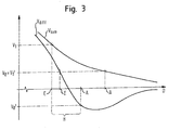
- FIG. 3 shows a further example of the arrangement of the threshold values of a foreground button, which essentially corresponds to the example according to FIG. 2.
- the lower difference threshold value V 0 ' has a negative value
- the upper difference threshold value V 1 ' - and with it the lower sum threshold value V 0 - is defined symmetrically with respect to the value zero.
- the path hysteresis H shown in FIG. 3 is obtained.
- both the relevant switch-on point E and the relevant switch-off point A change for the difference signals V diff of objects with different reflectivities.
- this change in the path hysteresis H takes place essentially symmetrical around the zero crossing of the difference signal V diff , the path hysteresis H for objects of greater reflectivity always being lower than the path hysteresis H for darker objects.
- Fig. 4 shows schematically a possible structure of the invention Sensor.
- This sensor has a transmitter 11 and a receiver 13, which with the transmitter 11 forms a triangulation arrangement and two receiving elements having.
- the receiver 13 can be act a differential diode that a near-reception signal and a far-reception signal emits.
- the two received signals are forwarded via a respective amplifier 15 to a differential stage 17 and to a summer 19.
- the output signal of the differential stage 17 is present at the positive input of a comparison device, namely a comparator 21, the negative input of which is optionally supplied with the lower differential threshold value V 0 'or the upper differential threshold value V 1 '.
- the output signal of the summer 19 and optionally the lower total threshold value V 0 and the upper total threshold value V 1 are fed to the two inputs of a further comparator 23.
- the output signals of the two comparators 21, 23 are logically linked by an AND gate 25.
- the AND gate 25 forwards the result of this combination to the switching input of a flip-flop 27.
- the object detection signal Q is generated, which is simultaneously used for switching between the lower and upper difference threshold V 0 'or V 1' and the lower and upper sum threshold value V0 or V1.
- a clock 29 feeds the transmitter 11 and the flip-flop 27 with one Rectangular pulse.
- the clock generator 29 causes the transmitter 11 to emit pulsed transmission light signals.
- the light reflected by an object located in the detection range of the sensor leads on the part of the receiver 13 to generate the two received signals which are converted into the difference signal V diff and the sum signal V sum .
- the switching structure of the sensor according to FIG. 4 is in particular because of this advantageous simply because the switching hysteresis by means of the most recently determined Item detection signal Q is controlled.
- the sensor according to FIG. 4 can also be developed in such a way that a Switching of the object detection signal Q takes place only if the switching condition provided for this during several successive Clocks of the clock generator 29 is satisfied.
- By such Design can be caused, for example, by external flash light Incorrect switching can be avoided.
- measures can also be provided in order to be able to set the switching distance.
- the position of the light spot on the receiver 13 can be adjusted by an adjustable receiver lens or a mirror in order to specify the distance at which the difference signal V diff assumes the value zero.
Landscapes
- Physics & Mathematics (AREA)
- Life Sciences & Earth Sciences (AREA)
- General Life Sciences & Earth Sciences (AREA)
- General Physics & Mathematics (AREA)
- Geophysics (AREA)
- Geophysics And Detection Of Objects (AREA)
- Measurement Of Optical Distance (AREA)
- Optical Radar Systems And Details Thereof (AREA)
- Electronic Switches (AREA)
- Light Receiving Elements (AREA)
Abstract
Description
- Fig. 1 und 5
- Differenzsignale in Abhängigkeit vom Tastabstand für Objekte unterschiedlichen Reflexionsvermögens,
- Fig. 2 und 3
- ein Differenz- und ein Summensignal in Abhängigkeit vom Tastabstand für unterschiedliche Schwellenwerte, und
- Fig. 4
- ein Blockschaltbild des erfindungsgemäßen Sensors.
- 11
- Sender
- 13
- Empfänger
- 15
- Verstärker
- 17
- Differenzstufe
- 19
- Summierer
- 21
- Komparator
- 23
- Komparator
- 25
- UND-Gatter
- 27
- Flip-Flop
- 29
- Taktgeber
- D
- Tastabstand
- E, ES, EW
- Einschaltpunkt
- A, AS, AW, A'
- Ausschaltpunkt
- H, HS, HW
- Weghysterese
- Q
- Gegenstandsfeststellungssignal
- S
- schwarzes Objekt
- W
- weißes Objekt
- Vdiff
- Differenzsignal
- Vsum
- Summensignal
- V0'
- unterer Differenzschwellenwert
- V1'
- oberer Differenzschwellenwert
- V0
- unterer Summenschwellenwert
- V1
- oberer Summenschwellenwert
Claims (14)
- Optoelektronischer Sensor, insbesondere Reflexionslichttaster, zumindest mitwobei zur Erzeugung einer Schalthysterese (H) mehrere verschiedene Schwellenwerte (V0', V1'; V0, V1) vorgesehen sind,einem Sender (11) zum Aussenden von Sendelicht,einem Empfänger (13) zur Ausgabe von wenigstens zwei Empfangssignalen in Abhängigkeit von reflektiertem und empfangenem Sendelicht, undeiner Auswerteeinrichtung, durch die zur Feststellung, ob sich ein Objekt oder kein Objekt in einem Erfassungsbereich des Sensors befindet, eine Differenz (Vdiff) der Empfangssignale mit einem Schwellenwert (V0', V1') vergleichbar ist und in Abhängigkeit von dem Ergebnis dieses Vergleichs ein positives oder negatives Gegenstandsfeststellungssignal (Q) erzeugbar ist,
dadurch gekennzeichnet, daß die Auswerteeinrichtung dergestalt ausgebildet ist, daß als zusätzliches Kriterium für die Erzeugung des Gegenstandsfeststellungssignals (Q) das Ergebnis eines Vergleichs einer Summe (Vsum) der Empfangssignale mit einem Schwellenwert (V0, V1) vorgesehen ist. - Sensor nach Anspruch 1,
dadurch gekennzeichnet, daß zur Erzeugung der Schalthysterese (H)vorgesehen sind.wenigstens zwei Schwellenwerte (V0', V1') für den Differenzvergleich (Differenzschwellenwerte) und wenigstens zwei Schwellenwerte (V0, V1) für den Summenvergleich (Summenschwellenwerte), oderwenigstens zwei Differenzschwellenwerte und ein einziger Summenschwellenwert, oderein einziger Differenzschwellenwert und wenigstens zwei Summenschwellenwerte - Sensor nach einem der vorangehenden Ansprüche,
dadurch gekennzeichnet, daß für einen Vergleich der Differenz (Vdiff) bzw. der Summe (Vsum) mit einem Schwellenwert jeweils einer der mehreren Schwellenwerte (V0', V1'; V0, V1) in Abhängigkeit von dem aktuellen Gegenstandsfeststellungssignal (Q) auswählbar ist. - Sensor nach einem der vorangehenden Ansprüche,
dadurch gekennzeichnet, daß als Bedingung für die Erzeugung eines negativen - oder eines positiven - Gegenstandsfeststellungssignals (Q) vorgesehen ist, daßentweder die Differenz (Vdiff) der Empfangssignale geringer ist als ein Differenzschwellenwert, insbesondere als ein unterer Differenzschwellenwert (V0'), oderdie Summe (Vsum) der Empfangssignale geringer ist als ein Summenschwellenwert, insbesondere als ein unterer Summenschwellenwert. - Sensor nach einem der vorangehenden Ansprüche,
dadurch gekennzeichnet, daß als Bedingung für die Erzeugung eines positiven - bzw. eines negativen - Gegenstandsfeststellungssignals (Q) vorgesehen ist, daßdie Differenz (Vdiff) der Empfangssignale größer ist als ein Differenzschwellenwert, insbesondere als ein oberer Differenzschwellenwert (V1'), unddie Summe (Vsum) der Empfangssignale größer ist als ein Summenschwellenwert, insbesondere als ein oberer Summenschwellenwert (V1). - Sensor nach einem der Ansprüche 1 bis 4,
dadurch gekennzeichnet, daß als Bedingung für die Erzeugung eines positiven - bzw. eines negativen - Gegenstandsfeststellungssignals (Q) vorgesehen ist, daß die Differenz (Vdiff) der Empfangssignale größer ist als ein Differenzschwellenwert, insbesondere als ein oberer Differenzschwellenwert (V1'). - Sensor nach einem der vorangehenden Ansprüche,
dadurch gekennzeichnet, daß ein Differenzschwellenwert (V0') Null oder im wesentlichen Null ist oder nahe des Wertes Null liegt. - Sensor nach einem der vorangehenden Ansprüche,
dadurch gekennzeichnet, daß zwei Differenzschwellenwerte (V0', V1') unterschiedliche Vorzeichen besitzen, und/oder
daß ein oberer Differenzschwellenwert (V1') und ein unterer Differenzschwellenwert (V0') im wesentlichen symmetrisch um den Wert Null angeordnet sind. - Sensor nach einem der vorangehenden Ansprüche,
dadurch gekennzeichnet, daß ein oberer Differenzschwellenwert (V1') einem unteren Summenschwellenwert (V0) entspricht, oder
daß der bzw. jeder Differenzschwellenwert und der bzw. jeder Summenschwellenwert unterschiedlich sind. - Sensor nach einem der vorangehenden Ansprüche,
dadurch gekennzeichnet, daß der Sender (11) und der Empfänger (13) eine Triangulationsanordnung bilden, und/oder
daß der Empfänger (13) zur Erzeugung der wenigstens zwei Empfangssignale mehrere Empfangsabschnitte oder Empfangselemente aufweist, und/oder
daß es sich bei den wenigstens zwei Empfangssignalen um ein Nah-Empfangssignal und ein Fern-Empfangssignal handelt. - Sensor nach einem der vorangehenden Ansprüche,
dadurch gekennzeichnet, daß der Sensor als Vordergrund-Taster oder als Hintergrund-Taster ausgebildet ist. - Sensor nach einem der vorangehenden Ansprüche,
dadurch gekennzeichnet, daß ein Taktgeber (29) vorgesehen ist, durch den der Sender (11) zum Aussenden von gepulstem Sendelicht ansteuerbar ist. - Sensor nach Anspruch 12,
dadurch gekennzeichnet, daß die Auswerteeinrichtung dergestalt ausgebildet ist, daß ein positives oder negatives Gegenstandsfeststellungssignal (Q) nur dann erzeugbar ist, wenn die jeweilige Bedingung während mehrerer aufeinanderfolgender Takte des Taktgebers (29) erfüllt ist. - Verfahren zur Erzeugung eines positiven oder negativen Gegenstandsfeststellungssignals (Q) in Abhängigkeit von dem Vorhandensein bzw. Nichtvorhandensein eines Objekts in einem Erfassungsbereich eines optoelektronischen Sensors,
insbesondere gemäß der Funktionsweise eines Sensors nach einem der vorhergehenden Ansprüche, wobeiwobei zur Erzeugung einer Schalthysterese (H) mehrere verschiedene Schwellenwerte (V0', V1'; V0, V1) berücksichtigt werden,Sendelicht in Richtung des Erfassungsbereichs ausgesendet wird,in Abhängigkeit von reflektiertem und empfangenem Sendelicht wenigstens zwei Empfangssignale erzeugt werden, undzur Erzeugung des positiven oder negativen Gegenstandsfeststellungssignals (Q) eine Differenz (Vdiff) der Empfangssignale mit einem Schwellenwert (V0', V1') verglichen wird,
dadurch gekennzeichnet, daß als zusätzliches Kriterium für die Erzeugung des Gegenstandsfeststellungssignals (Q) eine Summe (Vsum) der Empfangssignale mit einem Schwellenwert (V0, V1) verglichen wird.
Applications Claiming Priority (2)
| Application Number | Priority Date | Filing Date | Title |
|---|---|---|---|
| DE10131685 | 2001-06-29 | ||
| DE10131685A DE10131685A1 (de) | 2001-06-29 | 2001-06-29 | Optoelektronischer Sensor |
Publications (3)
| Publication Number | Publication Date |
|---|---|
| EP1271183A2 true EP1271183A2 (de) | 2003-01-02 |
| EP1271183A3 EP1271183A3 (de) | 2003-10-22 |
| EP1271183B1 EP1271183B1 (de) | 2006-10-11 |
Family
ID=7690105
Family Applications (1)
| Application Number | Title | Priority Date | Filing Date |
|---|---|---|---|
| EP02011871A Expired - Lifetime EP1271183B1 (de) | 2001-06-29 | 2002-05-28 | Optoelektronischer Sensor |
Country Status (5)
| Country | Link |
|---|---|
| US (1) | US6943338B2 (de) |
| EP (1) | EP1271183B1 (de) |
| JP (1) | JP2003084074A (de) |
| AT (1) | ATE342517T1 (de) |
| DE (2) | DE10131685A1 (de) |
Cited By (1)
| Publication number | Priority date | Publication date | Assignee | Title |
|---|---|---|---|---|
| WO2015128186A1 (de) * | 2014-02-25 | 2015-09-03 | Ifm Electronic Gmbh | Verfahren zum betreiben eines optischen näherungsschalters nach dem lichtlaufzeitprinzip |
Families Citing this family (10)
| Publication number | Priority date | Publication date | Assignee | Title |
|---|---|---|---|---|
| JP2006145483A (ja) * | 2004-11-24 | 2006-06-08 | Sharp Corp | パルス変調型光検出装置、電子機器、パルス変調型光検出方法 |
| DE102006032113C5 (de) * | 2006-07-11 | 2010-01-28 | Pepperl + Fuchs Gmbh | Optischer Triangulationssensor und Verfahren zum Testen eines optischen Triangulationssensors |
| JP5033034B2 (ja) * | 2008-03-27 | 2012-09-26 | 旭化成エレクトロニクス株式会社 | 赤外線センサ、赤外線センサを使った検知方法 |
| ATE533070T1 (de) | 2008-09-01 | 2011-11-15 | Sick Ag | Objektfeststellungsverfahren und objektfeststellungssensor |
| US20100163759A1 (en) * | 2008-12-31 | 2010-07-01 | Stmicroelectronics S.R.L. | Radiation sensor with photodiodes being integrated on a semiconductor substrate and corresponding integration process |
| IT1392502B1 (it) * | 2008-12-31 | 2012-03-09 | St Microelectronics Srl | Sensore comprendente almeno un fotodiodo a doppia giunzione verticale integrato su substrato semiconduttore e relativo processo di integrazione |
| DE202009002340U1 (de) | 2009-02-18 | 2010-07-08 | Pepperl + Fuchs Gmbh | Triangulationssensor |
| US10509114B2 (en) * | 2015-03-30 | 2019-12-17 | Sharp Kabushiki Kaisha | Photodetection device with synchronous and non-synchronous light detection for reducing noise and electronic apparatus |
| JP6990356B2 (ja) * | 2018-10-30 | 2022-01-12 | オムロン株式会社 | センサ装置及び検出方法 |
| US10401480B1 (en) * | 2018-12-05 | 2019-09-03 | Luminar Technologies, Inc. | Lidar receiver with multiple detectors for range-ambiguity mitigation |
Family Cites Families (11)
| Publication number | Priority date | Publication date | Assignee | Title |
|---|---|---|---|---|
| US1995557A (en) * | 1931-09-21 | 1935-03-26 | Durand & Huguenin Ag | Process of preparing sulphuric acid esters of leuco derivatives of vat dyestuffs |
| JPS56103310A (en) * | 1980-01-22 | 1981-08-18 | Nippon Telegr & Teleph Corp <Ntt> | System for controlling distance from target by using reflection type optical sensor |
| JPH07115773B2 (ja) * | 1986-01-29 | 1995-12-13 | 株式会社ニコン | 基板搬送装置 |
| JPH01170886A (ja) * | 1987-12-26 | 1989-07-05 | Chinon Ind Inc | 反射形光電スイッチ |
| JPH062348Y2 (ja) * | 1988-02-15 | 1994-01-19 | オムロン株式会社 | 反射型光電スイッチ |
| ATE320015T1 (de) * | 1997-12-17 | 2006-03-15 | Inter Company Computer Enginee | Vorrichtung zur feststellung von annäherungen |
| DE19808215C2 (de) * | 1998-02-27 | 2001-03-15 | Leuze Electronic Gmbh & Co | Optoelektronische Vorrichtung und Verfahren zu deren Betrieb |
| DE19907547B4 (de) * | 1998-03-17 | 2006-03-09 | Leuze Electronic Gmbh & Co Kg | Optoelektronische Vorrichtung |
| DE19951557B4 (de) * | 1998-10-30 | 2005-02-10 | Leuze Electronic Gmbh & Co Kg | Optoelektronische Vorrichtung |
| DE19852173C2 (de) * | 1998-11-12 | 2003-04-17 | Leuze Electronic Gmbh & Co | Lichttaster |
| DE20003675U1 (de) * | 1999-03-02 | 2000-06-08 | Leuze Electronic Gmbh + Co, 73277 Owen | Optoelektronische Vorrichtung |
-
2001
- 2001-06-29 DE DE10131685A patent/DE10131685A1/de not_active Withdrawn
-
2002
- 2002-05-28 EP EP02011871A patent/EP1271183B1/de not_active Expired - Lifetime
- 2002-05-28 AT AT02011871T patent/ATE342517T1/de not_active IP Right Cessation
- 2002-05-28 DE DE50208381T patent/DE50208381D1/de not_active Expired - Lifetime
- 2002-06-04 US US10/163,266 patent/US6943338B2/en not_active Expired - Lifetime
- 2002-07-01 JP JP2002192267A patent/JP2003084074A/ja active Pending
Cited By (4)
| Publication number | Priority date | Publication date | Assignee | Title |
|---|---|---|---|---|
| WO2015128186A1 (de) * | 2014-02-25 | 2015-09-03 | Ifm Electronic Gmbh | Verfahren zum betreiben eines optischen näherungsschalters nach dem lichtlaufzeitprinzip |
| CN106030338A (zh) * | 2014-02-25 | 2016-10-12 | Ifm电子股份有限公司 | 用于根据光-传播时间原则操作光学接近开关的方法 |
| US10145943B2 (en) | 2014-02-25 | 2018-12-04 | Ifm Electronic Gmbh | Method for operating an optical proximity switch in accordance with the time-of-flight principle |
| CN106030338B (zh) * | 2014-02-25 | 2019-03-12 | Ifm电子股份有限公司 | 用于根据光-传播时间原则操作光学接近开关的方法 |
Also Published As
| Publication number | Publication date |
|---|---|
| EP1271183B1 (de) | 2006-10-11 |
| ATE342517T1 (de) | 2006-11-15 |
| US6943338B2 (en) | 2005-09-13 |
| US20040099795A1 (en) | 2004-05-27 |
| DE10131685A1 (de) | 2003-01-16 |
| JP2003084074A (ja) | 2003-03-19 |
| DE50208381D1 (de) | 2006-11-23 |
| EP1271183A3 (de) | 2003-10-22 |
Similar Documents
| Publication | Publication Date | Title |
|---|---|---|
| EP1423731B1 (de) | Verfahren und vorrichtung zur aufnahme eines dreidimensionalen abstandsbildes | |
| DE10138609B4 (de) | Überwachungsverfahren und optoelektronischer Sensor | |
| DE3238022C2 (de) | Vorrichtung zum Erfassen sich bewegender Hindernisse für Fahrzeuge | |
| EP1271183B1 (de) | Optoelektronischer Sensor | |
| EP2088453B1 (de) | Optoelektronischer Sensor zur Entfernungsmessung | |
| DE4221113C1 (de) | Komparatorschaltung zur Auslösung eines Schaltvorganges beim Durchgang eines veränderlichen Meßsignals durch eine Schaltschwelle | |
| DE19701803A1 (de) | Lichttaster mit Lichtlaufzeit-Auswertung | |
| DE2636906B2 (de) | Verfahren zur Erzeugung eines Schaltsignals beim Durchgang eines Kontrastsprunges und Schaltungsanordnung zur Ausführung des Verfahrens | |
| DE1220055B (de) | Halbleiterdiode fuer optische Schaltung mit kohaerentem Licht und optische Schalteinrichtung dafuer | |
| DE3408261C2 (de) | ||
| DE102014220487A1 (de) | Fotoelektrischer Sensor | |
| DE102005046989B4 (de) | Fahrzeugradarsystem | |
| DE19808215C2 (de) | Optoelektronische Vorrichtung und Verfahren zu deren Betrieb | |
| EP4202580B1 (de) | Sensorschaltung für eine eine sicherheitsfunktion ausführende vorrichtung, vorrichtung und verfahren zum verarbeiten von messwerten von sensoren | |
| DE2933817A1 (de) | Automatische entfernungsmessvorrichtung | |
| DE19745493A1 (de) | Näherungssensor und Verfahren zur Personenerkennung | |
| DE19852173A1 (de) | Lichttaster | |
| DE2065927B2 (de) | Schwellwertschaltung | |
| DE19747248A1 (de) | Reflexionslichtschranke | |
| DE19917487A1 (de) | Optoelektronische Vorrichtung | |
| DE102020105112A1 (de) | Kraftfahrzeugbeleuchtungseinrichtung mit einem Lidarsensor und Verfahren zum Betreiben der Kraftfahrzeugbeleuchtungseinrichtung | |
| DE19951165C1 (de) | Optischer Sensor | |
| DE3005043C2 (de) | Automatische Fokussierungsanzeigevorrichtung für eine Kamera | |
| DE19753836A1 (de) | Fotozelle mit verriegelbarer Differenzverarbeitung | |
| DE102022120577A1 (de) | Vorrichtung und Verfahren zur Beleuchtung eines Fahrzeugvorfeldes |
Legal Events
| Date | Code | Title | Description |
|---|---|---|---|
| PUAI | Public reference made under article 153(3) epc to a published international application that has entered the european phase |
Free format text: ORIGINAL CODE: 0009012 |
|
| AK | Designated contracting states |
Kind code of ref document: A2 Designated state(s): AT BE CH CY DE DK ES FI FR GB GR IE IT LI LU MC NL PT SE TR |
|
| AX | Request for extension of the european patent |
Free format text: AL;LT;LV;MK;RO;SI |
|
| PUAL | Search report despatched |
Free format text: ORIGINAL CODE: 0009013 |
|
| AK | Designated contracting states |
Kind code of ref document: A3 Designated state(s): AT BE CH CY DE DK ES FI FR GB GR IE IT LI LU MC NL PT SE TR |
|
| AX | Request for extension of the european patent |
Extension state: AL LT LV MK RO SI |
|
| 17P | Request for examination filed |
Effective date: 20031203 |
|
| AKX | Designation fees paid |
Designated state(s): AT BE CH CY DE DK ES FI FR GB GR IE IT LI LU MC NL PT SE TR |
|
| 17Q | First examination report despatched |
Effective date: 20050406 |
|
| GRAP | Despatch of communication of intention to grant a patent |
Free format text: ORIGINAL CODE: EPIDOSNIGR1 |
|
| GRAS | Grant fee paid |
Free format text: ORIGINAL CODE: EPIDOSNIGR3 |
|
| GRAA | (expected) grant |
Free format text: ORIGINAL CODE: 0009210 |
|
| AK | Designated contracting states |
Kind code of ref document: B1 Designated state(s): AT BE CH CY DE DK ES FI FR GB GR IE IT LI LU MC NL PT SE TR |
|
| PG25 | Lapsed in a contracting state [announced via postgrant information from national office to epo] |
Ref country code: IT Free format text: LAPSE BECAUSE OF FAILURE TO SUBMIT A TRANSLATION OF THE DESCRIPTION OR TO PAY THE FEE WITHIN THE PRESCRIBED TIME-LIMIT;WARNING: LAPSES OF ITALIAN PATENTS WITH EFFECTIVE DATE BEFORE 2007 MAY HAVE OCCURRED AT ANY TIME BEFORE 2007. THE CORRECT EFFECTIVE DATE MAY BE DIFFERENT FROM THE ONE RECORDED. Effective date: 20061011 Ref country code: FI Free format text: LAPSE BECAUSE OF FAILURE TO SUBMIT A TRANSLATION OF THE DESCRIPTION OR TO PAY THE FEE WITHIN THE PRESCRIBED TIME-LIMIT Effective date: 20061011 Ref country code: IE Free format text: LAPSE BECAUSE OF FAILURE TO SUBMIT A TRANSLATION OF THE DESCRIPTION OR TO PAY THE FEE WITHIN THE PRESCRIBED TIME-LIMIT Effective date: 20061011 Ref country code: NL Free format text: LAPSE BECAUSE OF FAILURE TO SUBMIT A TRANSLATION OF THE DESCRIPTION OR TO PAY THE FEE WITHIN THE PRESCRIBED TIME-LIMIT Effective date: 20061011 |
|
| REG | Reference to a national code |
Ref country code: GB Ref legal event code: FG4D Free format text: NOT ENGLISH |
|
| REG | Reference to a national code |
Ref country code: CH Ref legal event code: EP |
|
| REG | Reference to a national code |
Ref country code: IE Ref legal event code: FG4D Free format text: LANGUAGE OF EP DOCUMENT: GERMAN |
|
| REF | Corresponds to: |
Ref document number: 50208381 Country of ref document: DE Date of ref document: 20061123 Kind code of ref document: P |
|
| PG25 | Lapsed in a contracting state [announced via postgrant information from national office to epo] |
Ref country code: DK Free format text: LAPSE BECAUSE OF FAILURE TO SUBMIT A TRANSLATION OF THE DESCRIPTION OR TO PAY THE FEE WITHIN THE PRESCRIBED TIME-LIMIT Effective date: 20070111 Ref country code: SE Free format text: LAPSE BECAUSE OF FAILURE TO SUBMIT A TRANSLATION OF THE DESCRIPTION OR TO PAY THE FEE WITHIN THE PRESCRIBED TIME-LIMIT Effective date: 20070111 |
|
| PG25 | Lapsed in a contracting state [announced via postgrant information from national office to epo] |
Ref country code: ES Free format text: LAPSE BECAUSE OF FAILURE TO SUBMIT A TRANSLATION OF THE DESCRIPTION OR TO PAY THE FEE WITHIN THE PRESCRIBED TIME-LIMIT Effective date: 20070122 |
|
| RAP2 | Party data changed (patent owner data changed or rights of a patent transferred) |
Owner name: SICK AG |
|
| PG25 | Lapsed in a contracting state [announced via postgrant information from national office to epo] |
Ref country code: PT Free format text: LAPSE BECAUSE OF FAILURE TO SUBMIT A TRANSLATION OF THE DESCRIPTION OR TO PAY THE FEE WITHIN THE PRESCRIBED TIME-LIMIT Effective date: 20070319 |
|
| NLV1 | Nl: lapsed or annulled due to failure to fulfill the requirements of art. 29p and 29m of the patents act | ||
| GBV | Gb: ep patent (uk) treated as always having been void in accordance with gb section 77(7)/1977 [no translation filed] |
Effective date: 20061011 |
|
| ET | Fr: translation filed | ||
| REG | Reference to a national code |
Ref country code: IE Ref legal event code: FD4D |
|
| PLBE | No opposition filed within time limit |
Free format text: ORIGINAL CODE: 0009261 |
|
| STAA | Information on the status of an ep patent application or granted ep patent |
Free format text: STATUS: NO OPPOSITION FILED WITHIN TIME LIMIT |
|
| 26N | No opposition filed |
Effective date: 20070712 |
|
| PG25 | Lapsed in a contracting state [announced via postgrant information from national office to epo] |
Ref country code: GB Free format text: LAPSE BECAUSE OF FAILURE TO SUBMIT A TRANSLATION OF THE DESCRIPTION OR TO PAY THE FEE WITHIN THE PRESCRIBED TIME-LIMIT Effective date: 20061011 |
|
| BERE | Be: lapsed |
Owner name: SICK A.G. Effective date: 20070531 |
|
| PG25 | Lapsed in a contracting state [announced via postgrant information from national office to epo] |
Ref country code: MC Free format text: LAPSE BECAUSE OF NON-PAYMENT OF DUE FEES Effective date: 20070531 |
|
| PG25 | Lapsed in a contracting state [announced via postgrant information from national office to epo] |
Ref country code: BE Free format text: LAPSE BECAUSE OF NON-PAYMENT OF DUE FEES Effective date: 20070531 |
|
| PG25 | Lapsed in a contracting state [announced via postgrant information from national office to epo] |
Ref country code: GR Free format text: LAPSE BECAUSE OF FAILURE TO SUBMIT A TRANSLATION OF THE DESCRIPTION OR TO PAY THE FEE WITHIN THE PRESCRIBED TIME-LIMIT Effective date: 20070112 |
|
| PG25 | Lapsed in a contracting state [announced via postgrant information from national office to epo] |
Ref country code: AT Free format text: LAPSE BECAUSE OF NON-PAYMENT OF DUE FEES Effective date: 20070528 |
|
| PG25 | Lapsed in a contracting state [announced via postgrant information from national office to epo] |
Ref country code: LU Free format text: LAPSE BECAUSE OF NON-PAYMENT OF DUE FEES Effective date: 20070528 Ref country code: CY Free format text: LAPSE BECAUSE OF FAILURE TO SUBMIT A TRANSLATION OF THE DESCRIPTION OR TO PAY THE FEE WITHIN THE PRESCRIBED TIME-LIMIT Effective date: 20061011 |
|
| PG25 | Lapsed in a contracting state [announced via postgrant information from national office to epo] |
Ref country code: TR Free format text: LAPSE BECAUSE OF FAILURE TO SUBMIT A TRANSLATION OF THE DESCRIPTION OR TO PAY THE FEE WITHIN THE PRESCRIBED TIME-LIMIT Effective date: 20061011 |
|
| REG | Reference to a national code |
Ref country code: FR Ref legal event code: PLFP Year of fee payment: 15 |
|
| REG | Reference to a national code |
Ref country code: FR Ref legal event code: PLFP Year of fee payment: 16 |
|
| PGFP | Annual fee paid to national office [announced via postgrant information from national office to epo] |
Ref country code: CH Payment date: 20170523 Year of fee payment: 16 |
|
| REG | Reference to a national code |
Ref country code: FR Ref legal event code: PLFP Year of fee payment: 17 |
|
| REG | Reference to a national code |
Ref country code: CH Ref legal event code: PL |
|
| PG25 | Lapsed in a contracting state [announced via postgrant information from national office to epo] |
Ref country code: LI Free format text: LAPSE BECAUSE OF NON-PAYMENT OF DUE FEES Effective date: 20180531 Ref country code: CH Free format text: LAPSE BECAUSE OF NON-PAYMENT OF DUE FEES Effective date: 20180531 |
|
| PGFP | Annual fee paid to national office [announced via postgrant information from national office to epo] |
Ref country code: IT Payment date: 20210531 Year of fee payment: 20 Ref country code: DE Payment date: 20210525 Year of fee payment: 20 Ref country code: FR Payment date: 20210521 Year of fee payment: 20 |
|
| REG | Reference to a national code |
Ref country code: DE Ref legal event code: R071 Ref document number: 50208381 Country of ref document: DE |