EP1267404A2 - Verpackung für ein elektronisches Bauelement - Google Patents
Verpackung für ein elektronisches Bauelement Download PDFInfo
- Publication number
- EP1267404A2 EP1267404A2 EP02012804A EP02012804A EP1267404A2 EP 1267404 A2 EP1267404 A2 EP 1267404A2 EP 02012804 A EP02012804 A EP 02012804A EP 02012804 A EP02012804 A EP 02012804A EP 1267404 A2 EP1267404 A2 EP 1267404A2
- Authority
- EP
- European Patent Office
- Prior art keywords
- metallic insert
- inserts
- metallic
- area
- electronic component
- Prior art date
- Legal status (The legal status is an assumption and is not a legal conclusion. Google has not performed a legal analysis and makes no representation as to the accuracy of the status listed.)
- Granted
Links
Images
Classifications
-
- H—ELECTRICITY
- H10—SEMICONDUCTOR DEVICES; ELECTRIC SOLID-STATE DEVICES NOT OTHERWISE PROVIDED FOR
- H10W—GENERIC PACKAGES, INTERCONNECTIONS, CONNECTORS OR OTHER CONSTRUCTIONAL DETAILS OF DEVICES COVERED BY CLASS H10
- H10W76/00—Containers; Fillings or auxiliary members therefor; Seals
- H10W76/10—Containers or parts thereof
- H10W76/12—Containers or parts thereof characterised by their shape
- H10W76/15—Containers comprising an insulating or insulated base
- H10W76/157—Containers comprising an insulating or insulated base having interconnections parallel to the insulating or insulated base
-
- H—ELECTRICITY
- H10—SEMICONDUCTOR DEVICES; ELECTRIC SOLID-STATE DEVICES NOT OTHERWISE PROVIDED FOR
- H10W—GENERIC PACKAGES, INTERCONNECTIONS, CONNECTORS OR OTHER CONSTRUCTIONAL DETAILS OF DEVICES COVERED BY CLASS H10
- H10W70/00—Package substrates; Interposers; Redistribution layers [RDL]
- H10W70/40—Leadframes
- H10W70/479—Leadframes on or in insulating or insulated package substrates, interposers, or redistribution layers
-
- H—ELECTRICITY
- H10—SEMICONDUCTOR DEVICES; ELECTRIC SOLID-STATE DEVICES NOT OTHERWISE PROVIDED FOR
- H10W—GENERIC PACKAGES, INTERCONNECTIONS, CONNECTORS OR OTHER CONSTRUCTIONAL DETAILS OF DEVICES COVERED BY CLASS H10
- H10W90/00—Package configurations
- H10W90/701—Package configurations characterised by the relative positions of pads or connectors relative to package parts
- H10W90/751—Package configurations characterised by the relative positions of pads or connectors relative to package parts of bond wires
- H10W90/756—Package configurations characterised by the relative positions of pads or connectors relative to package parts of bond wires between a chip and a stacked lead frame, conducting package substrate or heat sink
Definitions
- the invention is based on a packaging for electronic component according to the genre of the independent Claim.
- the packaging according to FIG. 1 has a plastic housing 100 in which Metal inserts 101 are embedded.
- This metallic Inserts are punched out of sheet metal and are used in the manufacture of the plastic housing 100 in the plastic mass embedded. This is done by the Plastic housing 100 are manufactured by injection molding and into the injection mold before filling with plastic metallic inserts 100 are inserted. After this These inserts 101 are then used to fill the injection mold firmly embedded in the plastic material of the housing 100.
- an electronic component is shown in FIG 102 shown, which with bond wires 103 with the Metal inserts 101 is electrically connected.
- the Bond wires 103 are elastic and can thus when the component 102 moves relative to the inserts 101 or relative to the housing 100 be deformed accordingly.
- a direct connection between the electronic components 102 with the inserts 101 problematic because of the different Expansion coefficient of the materials used, especially the plastic of the housing and the metallic components 101, it too different thermal expansion of the materials involved comes.
- a rigid connection between the inserts and the electronic components 102 would therefore have to have large forces endure by the different thermal Expansion coefficients are caused.
- the Connection between the electronic components 102 and the inserts 101 would be at great risk as this Connection usually by a solder or a conductive Glue is made that is not designed to absorb large forces are suitable.
- the packaging according to the invention for an electronic Component has the advantage that metallic carriers, which in the plastic material are embedded, directly with the electronic components can be connected.
- the additional connection via the bond wires can therefore omitted and such packaging can therefore be special be manufactured easily and inexpensively. Will continue through the direct coupling of the electronic component dissipation of heat with the metallic support improved.
- the elastic carrier is designed particularly simply by Formation of a meandering structure.
- the electronic Components can also be placed directly between two beams be mounted, which then expediently the same Form contacts. This is particularly easy Attachment by solder or glue. It becomes particularly easy the metallic support as a stamped part made of sheet metal developed.
- the plastic carrier becomes particularly simple made by injection molding.
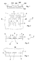
- FIG. 1 shows a cross section through a conventional packaging
- Figure 2 is a plan view of a Packaging according to the invention
- Figure 3 shows a cross section through Figure 2
- Figure 4 shows an intermediate step of Manufacturing process.
- FIG. 2 shows a supervision of the invention Packaging for an electronic component shown.
- the packaging has a plastic housing 1, in the metallic inserts 2 are embedded.
- the metallic inserts 2 extend in part in a They are recess 3 of the plastic housing 1 and in part the plastic mass of the plastic housing 1 enclosed.
- the areas where the metallic Insert parts from the plastic of the plastic housing 1 are enclosed in the following as embedding areas 4 designated.
- an electronic component 6 on the metallic inserts 2 attached is attached.
- the area where the electronic component 6 is attached in Hereinafter referred to as the fastening area 5.
- the plastic housing Under the inserts 2 in the area of the recess 3 the plastic housing is designed as a base 8, which itself extends under the entire area of the recess 3. Between the bottom 8 and the inserts 2 is a small distance 9 is provided. The size of this distance is mainly determined by the fact that in the production of the plastic housing 1 a certain shrinkage of the Plastic material takes place, which then the distance 9th between the inserts 2 and the bottom 8 results. This Distance 9 can be very small, so that the inserts in Essentially lie on the floor 8.
- the bottom 8 is not necessarily plan, in particular they can Areas over which the inserts 2 are not arranged are deepened. It depends on that Manufacturing process together as shown in Figure 4 is further explained.
- the Inserts 2 meandering. Through this it becomes meandering structure of the insert parts 2 enables the inserts 2 in the area of Recess 3 relative to the plastic housing 1 in the lateral Can move direction. This is particularly important because the coefficient of thermal expansion of the metallic inserts 2 and the material of the Strongly differentiate plastic housing 1. Through this different thermal expansion coefficient comes there is mechanical tension in the event of temperature changes between the plastic housing 1 and the metallic Inserts 2. Furthermore, mechanical Tensions between the two metal inserts 2 occur because they are held by the plastic housing 1 become.
- a component 6 was shown here, which is between two Inserts 2 is arranged. But the invention is equally useful if the component 6 only on one Insert or connected to more than two inserts is. It is always important that between the Junction of the insert 2 with the component and a laterally deformable area in the plastic housing is arranged.
- FIG. 4 shows the production of the invention Packaging explained. It is a cross section through the Packaging according to the invention during injection molding shown. In the cross section in Figure 4 is a Cross section through the plastic housing 1 and a Insert 2 shown during injection molding. The Cross section corresponds to the same place as in the Figure 2 is shown.
- the cavity 3 of FIG. 3 during injection molding from a mold 20 filled.
- the molding tool 20 is shaped so that it not only fills the cavity 3, but also that it the space around the inserts 2 towards the floor 8 completely filled out. In this way, those shown in FIG shown wells introduced. That way prevents the plastic mass from moving even in the XY plane between different areas of the inserts 2 arranges. If there is plastic mass there, mobility, i.e.
- the special molding tool 20 prevents the Injection molding between individual areas of the inserts 2 Plastic material accumulates, which causes deformation of the Inserts 2 could hinder in the XY plane.
Landscapes
- Injection Moulding Of Plastics Or The Like (AREA)
- Packaging Of Annular Or Rod-Shaped Articles, Wearing Apparel, Cassettes, Or The Like (AREA)
Abstract
Description
Claims (6)
- Verpackung für ein elektronisches Bauelement (6) mit einem metallischen Einlegeteil (2) und einem Kunststoffgehäuse (1), in dem das metallische Einlegeteil (2) mit einem Einbettbereich (4) eingebettet ist, wobei eine Dicke des metallischen Einlegeteils (2) gering ist im Vergleich zur lateralen Abmessung, dadurch gekennzeichnet, dass auf dem metallischen Einlegeteil (2) das Bauelement (6) auf einem Befestigungsbereich (5) befestigt ist, dass das metallische Einlegeteil zwischen Einbettbereich (4) und Befestigungsbereich (5) in lateraler Richtung verformbar ausgebildet ist und dass der Kunststoffträger (1) einen Boden (8) aufweist, der sich unter dem Befestigungsbereich (5) des metallischen Einlegeteils (2) mit einem Abstand (9) erstreckt, der geringer ist als die Dicke des metallischen Einlegeteils (2).
- Verpackung nach Anspruch 1, dadurch gekennzeichnet, dass das metallische Einlegeteile (2) zwischen Einbettbereich (4) und Befestigungsbereich (5) als mäanderartige Struktur ausgebildet ist.
- Verpackung nach Anspruch 1 oder 2, dadurch gekennzeichnet, dass mindestens zwei metallische Einlegeteile (2) vorgesehen sind, die jeweils einen Befestigungsbereich (5) aufweisen und dass das elektronische Bauelement (6) auf beiden Befestigungsbereichen (5) befestigt ist.
- Verpackung nach einem der vorhergehenden Ansprüche, dadurch gekennzeichnet, dass die Befestigung des elektronischen Bauelements (6) auf den Befestigungsbereichen durch ein Lot (7) oder einen Kleber (7) erfolgt.
- Verpackung nach einem der vorhergehenden Ansprüche, dadurch gekennzeichnet, dass das metallische Einlegeteil durch Stanzen eines Metallblechs gebildet ist.
- Verpackung nach einem der vorhergehenden Ansprüche, dadurch gekennzeichnet, dass das Kunststoffgehäuse (1) durch Spritzguß einer Kunststoffmasse in einer Form gebildet ist.
Applications Claiming Priority (2)
| Application Number | Priority Date | Filing Date | Title |
|---|---|---|---|
| DE10128756 | 2001-06-13 | ||
| DE10128756A DE10128756A1 (de) | 2001-06-13 | 2001-06-13 | Verpackung für ein elektronisches Bauelement |
Publications (3)
| Publication Number | Publication Date |
|---|---|
| EP1267404A2 true EP1267404A2 (de) | 2002-12-18 |
| EP1267404A3 EP1267404A3 (de) | 2004-12-08 |
| EP1267404B1 EP1267404B1 (de) | 2007-05-09 |
Family
ID=7688193
Family Applications (1)
| Application Number | Title | Priority Date | Filing Date |
|---|---|---|---|
| EP02012804A Expired - Lifetime EP1267404B1 (de) | 2001-06-13 | 2002-06-10 | Verpackung für ein elektronisches Bauelement |
Country Status (2)
| Country | Link |
|---|---|
| EP (1) | EP1267404B1 (de) |
| DE (2) | DE10128756A1 (de) |
Family Cites Families (4)
| Publication number | Priority date | Publication date | Assignee | Title |
|---|---|---|---|---|
| US3947867A (en) * | 1970-12-21 | 1976-03-30 | Signetics Corporation | Two part package for a semiconductor die |
| EP0452634B1 (de) * | 1990-03-16 | 1997-05-02 | Sumitomo Electric Industries, Ltd. | Leiterrahmen für Halbleiteranordnung |
| JPH0964266A (ja) * | 1995-08-18 | 1997-03-07 | Sony Corp | リードフレーム |
| JP2001024132A (ja) * | 1999-06-30 | 2001-01-26 | Texas Instr Inc <Ti> | 半導体デバイス用変形吸収形リードフレーム |
-
2001
- 2001-06-13 DE DE10128756A patent/DE10128756A1/de not_active Withdrawn
-
2002
- 2002-06-10 DE DE50210102T patent/DE50210102D1/de not_active Expired - Lifetime
- 2002-06-10 EP EP02012804A patent/EP1267404B1/de not_active Expired - Lifetime
Also Published As
| Publication number | Publication date |
|---|---|
| DE10128756A1 (de) | 2002-12-19 |
| EP1267404A3 (de) | 2004-12-08 |
| DE50210102D1 (de) | 2007-06-21 |
| EP1267404B1 (de) | 2007-05-09 |
Similar Documents
| Publication | Publication Date | Title |
|---|---|---|
| DE69918038T2 (de) | Ein mit Kunststoff umhülltes elektronisches Bauelement | |
| EP1697175B1 (de) | Steuergeräteeinheit und verfahren zur herstellung derselben | |
| CH686325A5 (de) | Elektronikmodul und Chip-Karte. | |
| DE69615792T2 (de) | Miniatur-halbleiteranordnung für oberflächenmontage | |
| DE69534483T2 (de) | Leiterrahmen und Halbleiterbauelement | |
| DE102006016775A1 (de) | Elektronische Vorrichtung und Verfahren zum Herstellen der Gleichen | |
| EP1040321B1 (de) | Messwertaufnehmer und ein verfahren zu dessen herstellung | |
| DE10012169B4 (de) | Druckerfassungsvorrichtung, Verfahren zu deren Herstellung und Gießvorrichtung | |
| DE3438435C2 (de) | Gehäuse aus Metall und Kunststoff für eine Halbleiter-Vorrichtung, das zur Befestigung an einem nicht genau ebenen Wärmeableiter geeignet ist, sowie Verfahren zu dessen Herstellung | |
| DE19609679C2 (de) | Verbundteil | |
| DE69409662T2 (de) | Elektrischer verbinder zur oberflächenmontage auf einer leiterplatte | |
| DE102022110325A1 (de) | Halbleitervorrichtung und Verfahren zum Herstellen einer Halbleitervorrichtung | |
| DE102017219410A1 (de) | Bauteilverbund und Steuergerät | |
| DE102019201404A1 (de) | Elektronikmodul | |
| EP0907966B1 (de) | Integrierte halbleiterschaltung | |
| EP1267404B1 (de) | Verpackung für ein elektronisches Bauelement | |
| DE69524312T2 (de) | Verfahren zur herstellung eines vergossenen leiterrahmens | |
| EP3520585B1 (de) | Verfahren zum herstellen einer elektronischen baugruppe und elektronische baugruppe, insbesondere für ein getriebesteuermodul | |
| DE102005007643A1 (de) | Verfahren und Anordnung zum Kontaktieren von Halbleiterchips auf einem metallischen Substrat | |
| DE19730166A1 (de) | Transponderanordnung und Verfahren zu deren Herstellung | |
| DE102005012496B3 (de) | Vorrichtung mit einem auf einem Montageteil montierten elektronischen Bauteil und Verfahren | |
| DE112020006695B4 (de) | Halbleitervorrichtung und Herstellungsverfahren einer Halbleitervorrichtung | |
| DE102021101895A1 (de) | Halbleitervorrichtung und Verfahren zu deren Herstellung | |
| DE2926008A1 (de) | Verbundformteil | |
| EP0642165A2 (de) | Hybridrahmen |
Legal Events
| Date | Code | Title | Description |
|---|---|---|---|
| PUAI | Public reference made under article 153(3) epc to a published international application that has entered the european phase |
Free format text: ORIGINAL CODE: 0009012 |
|
| AK | Designated contracting states |
Kind code of ref document: A2 Designated state(s): AT BE CH CY DE DK ES FI FR GB GR IE IT LI LU MC NL PT SE TR |
|
| AX | Request for extension of the european patent |
Free format text: AL;LT;LV;MK;RO;SI |
|
| PUAL | Search report despatched |
Free format text: ORIGINAL CODE: 0009013 |
|
| RIC1 | Information provided on ipc code assigned before grant |
Ipc: 7H 01L 23/498 A Ipc: 7H 01L 23/495 B |
|
| AK | Designated contracting states |
Kind code of ref document: A3 Designated state(s): AT BE CH CY DE DK ES FI FR GB GR IE IT LI LU MC NL PT SE TR |
|
| AX | Request for extension of the european patent |
Extension state: AL LT LV MK RO SI |
|
| 17P | Request for examination filed |
Effective date: 20050608 |
|
| AKX | Designation fees paid |
Designated state(s): DE FR GB IT |
|
| GRAP | Despatch of communication of intention to grant a patent |
Free format text: ORIGINAL CODE: EPIDOSNIGR1 |
|
| GRAS | Grant fee paid |
Free format text: ORIGINAL CODE: EPIDOSNIGR3 |
|
| GRAA | (expected) grant |
Free format text: ORIGINAL CODE: 0009210 |
|
| AK | Designated contracting states |
Kind code of ref document: B1 Designated state(s): DE FR GB IT |
|
| REG | Reference to a national code |
Ref country code: GB Ref legal event code: FG4D Free format text: NOT ENGLISH |
|
| REF | Corresponds to: |
Ref document number: 50210102 Country of ref document: DE Date of ref document: 20070621 Kind code of ref document: P |
|
| GBT | Gb: translation of ep patent filed (gb section 77(6)(a)/1977) |
Effective date: 20070718 |
|
| ET | Fr: translation filed | ||
| PLBE | No opposition filed within time limit |
Free format text: ORIGINAL CODE: 0009261 |
|
| STAA | Information on the status of an ep patent application or granted ep patent |
Free format text: STATUS: NO OPPOSITION FILED WITHIN TIME LIMIT |
|
| 26N | No opposition filed |
Effective date: 20080212 |
|
| PGFP | Annual fee paid to national office [announced via postgrant information from national office to epo] |
Ref country code: FR Payment date: 20110630 Year of fee payment: 10 |
|
| PGFP | Annual fee paid to national office [announced via postgrant information from national office to epo] |
Ref country code: GB Payment date: 20110621 Year of fee payment: 10 |
|
| PGFP | Annual fee paid to national office [announced via postgrant information from national office to epo] |
Ref country code: IT Payment date: 20110627 Year of fee payment: 10 |
|
| GBPC | Gb: european patent ceased through non-payment of renewal fee |
Effective date: 20120610 |
|
| PG25 | Lapsed in a contracting state [announced via postgrant information from national office to epo] |
Ref country code: IT Free format text: LAPSE BECAUSE OF NON-PAYMENT OF DUE FEES Effective date: 20120610 |
|
| REG | Reference to a national code |
Ref country code: FR Ref legal event code: ST Effective date: 20130228 |
|
| PG25 | Lapsed in a contracting state [announced via postgrant information from national office to epo] |
Ref country code: FR Free format text: LAPSE BECAUSE OF NON-PAYMENT OF DUE FEES Effective date: 20120702 Ref country code: GB Free format text: LAPSE BECAUSE OF NON-PAYMENT OF DUE FEES Effective date: 20120610 |
|
| PGFP | Annual fee paid to national office [announced via postgrant information from national office to epo] |
Ref country code: DE Payment date: 20140808 Year of fee payment: 13 |
|
| REG | Reference to a national code |
Ref country code: DE Ref legal event code: R119 Ref document number: 50210102 Country of ref document: DE |
|
| PG25 | Lapsed in a contracting state [announced via postgrant information from national office to epo] |
Ref country code: DE Free format text: LAPSE BECAUSE OF NON-PAYMENT OF DUE FEES Effective date: 20160101 |