EP1259060B1 - Bebilderungseinrichtung zur Erzeugung einer Anzahl von Bildpunkten in einer Projektionslinie - Google Patents
Bebilderungseinrichtung zur Erzeugung einer Anzahl von Bildpunkten in einer Projektionslinie Download PDFInfo
- Publication number
- EP1259060B1 EP1259060B1 EP02009280A EP02009280A EP1259060B1 EP 1259060 B1 EP1259060 B1 EP 1259060B1 EP 02009280 A EP02009280 A EP 02009280A EP 02009280 A EP02009280 A EP 02009280A EP 1259060 B1 EP1259060 B1 EP 1259060B1
- Authority
- EP
- European Patent Office
- Prior art keywords
- diode laser
- laser light
- light source
- light sources
- line
- Prior art date
- Legal status (The legal status is an assumption and is not a legal conclusion. Google has not performed a legal analysis and makes no representation as to the accuracy of the status listed.)
- Expired - Lifetime
Links
- 238000003384 imaging method Methods 0.000 title claims description 95
- 238000000034 method Methods 0.000 claims abstract description 13
- 230000003111 delayed effect Effects 0.000 claims description 13
- 230000001960 triggered effect Effects 0.000 abstract description 9
- 230000033001 locomotion Effects 0.000 description 10
- 230000000694 effects Effects 0.000 description 8
- 230000003287 optical effect Effects 0.000 description 8
- 238000012937 correction Methods 0.000 description 7
- 230000004075 alteration Effects 0.000 description 4
- 238000003491 array Methods 0.000 description 4
- 238000001816 cooling Methods 0.000 description 4
- 230000006870 function Effects 0.000 description 4
- 230000004913 activation Effects 0.000 description 3
- 230000008859 change Effects 0.000 description 3
- 238000013461 design Methods 0.000 description 3
- 230000008569 process Effects 0.000 description 3
- 239000004065 semiconductor Substances 0.000 description 3
- 238000012546 transfer Methods 0.000 description 3
- RYGMFSIKBFXOCR-UHFFFAOYSA-N Copper Chemical compound [Cu] RYGMFSIKBFXOCR-UHFFFAOYSA-N 0.000 description 2
- 229910052802 copper Inorganic materials 0.000 description 2
- 239000010949 copper Substances 0.000 description 2
- 238000011161 development Methods 0.000 description 2
- 230000018109 developmental process Effects 0.000 description 2
- 238000006073 displacement reaction Methods 0.000 description 2
- 230000005855 radiation Effects 0.000 description 2
- 230000009467 reduction Effects 0.000 description 2
- 238000007493 shaping process Methods 0.000 description 2
- 201000009310 astigmatism Diseases 0.000 description 1
- 230000005540 biological transmission Effects 0.000 description 1
- 239000000498 cooling water Substances 0.000 description 1
- 238000004519 manufacturing process Methods 0.000 description 1
- 238000005259 measurement Methods 0.000 description 1
- 230000010287 polarization Effects 0.000 description 1
- 230000002028 premature Effects 0.000 description 1
- 230000035945 sensitivity Effects 0.000 description 1
- 238000005476 soldering Methods 0.000 description 1
- 239000000126 substance Substances 0.000 description 1
- 239000000758 substrate Substances 0.000 description 1
Images


Classifications
-
- B—PERFORMING OPERATIONS; TRANSPORTING
- B41—PRINTING; LINING MACHINES; TYPEWRITERS; STAMPS
- B41J—TYPEWRITERS; SELECTIVE PRINTING MECHANISMS, i.e. MECHANISMS PRINTING OTHERWISE THAN FROM A FORME; CORRECTION OF TYPOGRAPHICAL ERRORS
- B41J2/00—Typewriters or selective printing mechanisms characterised by the printing or marking process for which they are designed
- B41J2/435—Typewriters or selective printing mechanisms characterised by the printing or marking process for which they are designed characterised by selective application of radiation to a printing material or impression-transfer material
- B41J2/447—Typewriters or selective printing mechanisms characterised by the printing or marking process for which they are designed characterised by selective application of radiation to a printing material or impression-transfer material using arrays of radiation sources
- B41J2/45—Typewriters or selective printing mechanisms characterised by the printing or marking process for which they are designed characterised by selective application of radiation to a printing material or impression-transfer material using arrays of radiation sources using light-emitting diode [LED] or laser arrays
-
- B—PERFORMING OPERATIONS; TRANSPORTING
- B41—PRINTING; LINING MACHINES; TYPEWRITERS; STAMPS
- B41C—PROCESSES FOR THE MANUFACTURE OR REPRODUCTION OF PRINTING SURFACES
- B41C1/00—Forme preparation
-
- B—PERFORMING OPERATIONS; TRANSPORTING
- B41—PRINTING; LINING MACHINES; TYPEWRITERS; STAMPS
- B41J—TYPEWRITERS; SELECTIVE PRINTING MECHANISMS, i.e. MECHANISMS PRINTING OTHERWISE THAN FROM A FORME; CORRECTION OF TYPOGRAPHICAL ERRORS
- B41J2/00—Typewriters or selective printing mechanisms characterised by the printing or marking process for which they are designed
- B41J2/435—Typewriters or selective printing mechanisms characterised by the printing or marking process for which they are designed characterised by selective application of radiation to a printing material or impression-transfer material
- B41J2/47—Typewriters or selective printing mechanisms characterised by the printing or marking process for which they are designed characterised by selective application of radiation to a printing material or impression-transfer material using the combination of scanning and modulation of light
- B41J2/471—Typewriters or selective printing mechanisms characterised by the printing or marking process for which they are designed characterised by selective application of radiation to a printing material or impression-transfer material using the combination of scanning and modulation of light using dot sequential main scanning by means of a light deflector, e.g. a rotating polygonal mirror
- B41J2/473—Typewriters or selective printing mechanisms characterised by the printing or marking process for which they are designed characterised by selective application of radiation to a printing material or impression-transfer material using the combination of scanning and modulation of light using dot sequential main scanning by means of a light deflector, e.g. a rotating polygonal mirror using multiple light beams, wavelengths or colours
-
- H—ELECTRICITY
- H04—ELECTRIC COMMUNICATION TECHNIQUE
- H04N—PICTORIAL COMMUNICATION, e.g. TELEVISION
- H04N1/00—Scanning, transmission or reproduction of documents or the like, e.g. facsimile transmission; Details thereof
- H04N1/04—Scanning arrangements, i.e. arrangements for the displacement of active reading or reproducing elements relative to the original or reproducing medium, or vice versa
- H04N1/047—Detection, control or error compensation of scanning velocity or position
- H04N1/053—Detection, control or error compensation of scanning velocity or position in main scanning direction, e.g. synchronisation of line start or picture elements in a line
-
- B—PERFORMING OPERATIONS; TRANSPORTING
- B41—PRINTING; LINING MACHINES; TYPEWRITERS; STAMPS
- B41C—PROCESSES FOR THE MANUFACTURE OR REPRODUCTION OF PRINTING SURFACES
- B41C1/00—Forme preparation
- B41C1/10—Forme preparation for lithographic printing; Master sheets for transferring a lithographic image to the forme
- B41C1/1075—Mechanical aspects of on-press plate preparation
-
- H—ELECTRICITY
- H04—ELECTRIC COMMUNICATION TECHNIQUE
- H04N—PICTORIAL COMMUNICATION, e.g. TELEVISION
- H04N1/00—Scanning, transmission or reproduction of documents or the like, e.g. facsimile transmission; Details thereof
- H04N1/04—Scanning arrangements, i.e. arrangements for the displacement of active reading or reproducing elements relative to the original or reproducing medium, or vice versa
- H04N1/06—Scanning arrangements, i.e. arrangements for the displacement of active reading or reproducing elements relative to the original or reproducing medium, or vice versa using cylindrical picture-bearing surfaces, i.e. scanning a main-scanning line substantially perpendicular to the axis and lying in a curved cylindrical surface
-
- H—ELECTRICITY
- H04—ELECTRIC COMMUNICATION TECHNIQUE
- H04N—PICTORIAL COMMUNICATION, e.g. TELEVISION
- H04N1/00—Scanning, transmission or reproduction of documents or the like, e.g. facsimile transmission; Details thereof
- H04N1/04—Scanning arrangements, i.e. arrangements for the displacement of active reading or reproducing elements relative to the original or reproducing medium, or vice versa
- H04N1/19—Scanning arrangements, i.e. arrangements for the displacement of active reading or reproducing elements relative to the original or reproducing medium, or vice versa using multi-element arrays
- H04N1/191—Scanning arrangements, i.e. arrangements for the displacement of active reading or reproducing elements relative to the original or reproducing medium, or vice versa using multi-element arrays the array comprising a one-dimensional array, or a combination of one-dimensional arrays, or a substantially one-dimensional array, e.g. an array of staggered elements
- H04N1/1911—Simultaneously or substantially simultaneously scanning picture elements on more than one main scanning line, e.g. scanning in swaths
-
- H—ELECTRICITY
- H04—ELECTRIC COMMUNICATION TECHNIQUE
- H04N—PICTORIAL COMMUNICATION, e.g. TELEVISION
- H04N2201/00—Indexing scheme relating to scanning, transmission or reproduction of documents or the like, and to details thereof
- H04N2201/04—Scanning arrangements
- H04N2201/047—Detection, control or error compensation of scanning velocity or position
- H04N2201/04753—Control or error compensation of scanning position or velocity
- H04N2201/04758—Control or error compensation of scanning position or velocity by controlling the position of the scanned image area
- H04N2201/04767—Control or error compensation of scanning position or velocity by controlling the position of the scanned image area by controlling the timing of the signals, e.g. by controlling the frequency o phase of the pixel clock
- H04N2201/04781—Controlling the phase of the signals
- H04N2201/04786—Controlling a start time, e.g. for output of a line of data
Definitions
- the invention relates to an imaging device with a number of light sources, each having a distance s i , the index i counting the light sources, to an object line, for generating pixels of the light sources in a projection line of the object line on a printing form, which at least with a velocity component v moves perpendicular to the direction defined by the projection line and tangential to the surface of the printing plate, and with a driving means for switching each individual light source.
- a plurality of light sources typically lasers, in particular diode laser arrays, are frequently used.
- Such a compact beam laser light source is in the document EP 1168 813 A2 disclosed.
- each individual light source or each individual emitter is switched on, or the quantities influencing light intensity are set or predetermined for each pressure point to be set in such a way that each individual emitter generates a pixel with a specific light intensity.
- an imaging optics for projecting the light emitted by the light sources onto the printing form, frequently with a change in the direction of propagation of the light or under beam shaping is also frequently provided.
- the pixels of the light sources on the printing form it is desirable for the pixels of the light sources on the printing form to lie in a projection line, typically when the printing form is recorded on a so-called printing plate cylinder or printing plate cylinder, parallel to the cylinder axis. If the pixels are not on a projection line or, in particular, not parallel to the cylinder axis, image errors can occur on the printing form.
- a compact laser diode array with reduced asymmetry is disclosed. It is contemplated to reduce the smile effect of the laser diode bar by associating a plurality of thermal load elements for the plurality of individual diode light sources.
- the thermal load elements are similar to the individual laser diode light sources except that their output power is blocked.
- Each thermal load element is brought into direct contact with its associated individual laser diodes, so that an efficient heat transfer can take place.
- By passing a variable current through the load element the operating temperature of the individual laser light source can be changed or adjusted. Consequently, the position of two laser light sources to each other by means of different currents can be achieved by their respective associated heat load.
- a disadvantage of a temperature influence of the smile effect is, for example, that the wavelength of the radiation emitted by the laser light source is changed. Furthermore, fluctuations in the temperature control lead to shifts in the position of the laser diode compared to the array axis.
- the light sources are turned on and off after a certain time.
- the emitters are triggered by a trigger signal or trigger signal at a certain triggering time. It is already known that, since the printing form having a velocity component v is perpendicular to the main direction of propagation of the light emitted by the light source
- the object line lies in the object plane.
- the object line may be a curve in the object plane with curved and straight sections, without limitation of generality, a straight object line will subsequently be considered.
- the individual light sources or emitters each have a distance s i , wherein i counts down the individual emitters, wherein at least two light sources have a different distance from the object line. Typically, this distance is not zero within the desired or required precision or can not be neglected.
- the laser diode bar has a plurality of light sources which emit light of different divergence in two mutually orthogonal axes, a so-called slow and a so-called fast axis, and illuminate an array of microlenses.
- the arrangement of microlenses collimates the light in the direction of the slow axis.
- An optical element adjacent to the microlenses breaks the light in the fast axis direction.
- an optical element In the direction of the slow axis, an optical element focuses the emitted one Moves light fixed direction, the pixel of a light source is depending on the triggering time on the printing form at a position with coordinates, which are a function of the triggering time.
- this fact is reflected in the document US Pat. No. 5,174,205 Device for the control of an imaging device for a printing form, which moves during the imaging process relative to the imaging device exploited.
- the image information is stored in a first memory, while correction data for the control of the light sources are in a second memory.
- the correction data is used to vary the time intervals between imaging shots of the light sources to compensate for deviations between the measured position of the printing form compared to the imaging head and the actual position.
- an imaging device incorporates a number of light sources
- a variation of the control of individual light sources thus serves at most to the position of the pixel on which at least one speed component v perpendicular to change or influence the main propagation direction of the direction determined by the light source emitted light moving form.
- an imaging of a printing form can take place by means of laser light sources lying along an object line via a transmission pattern of a lighted modulator or via the modulation of the pump currents when the laser light sources can be individually modulated.
- the surface of a printing form is moved with a velocity component v perpendicular to one through the projection line of the laser light sources or the exit points of the laser light from the modulator.
- a write head is described with a diode laser array individually addressable by a driver.
- the diode lasers are arranged along a straight line, which is preferably aligned parallel to the axis of rotation of a cylinder on which pixels in a projection line on a film are to be described.
- the cylinder is rotatable so that the projected pixels move relatively and tangentially to the surface of the film.
- the object of the present invention is to provide a printing device imaging device which has a number of pixels which are projected onto a projection line of an object line, with a plurality of diode laser light sources on a diode laser bar, at least two diode lasers on the diode laser bar being at a different distance from the object line.
- imaging device having the features according to claim 1 and by a method for generating pixels according to claim 5.
- Advantageous embodiments and further developments of the imaging device according to the invention and of the method according to the invention are characterized in the subclaims.
- the imaging device comprises a number of light sources for generating pixels of the light sources in a projection line on a printing form.
- the light sources each have a distance s i , where the subscript i counts down the light sources, to an object line in the object plane defined by the light sources.
- the end mirrors of the laser resonators essentially lie in one plane and can thus define an object plane.
- an object plane can also be a plane spatially behind an imaging optics arranged downstream of the light sources.
- the projection line comprises the dots of the printing form on which the image of the object line comes to rest on the printing form at a first point in time.
- Projection line and object line have a projection ratio k.
- a pixel of a light source is to be understood as that point on the printing form to which the light emitted by the light source strikes at a certain point in time while the light source is actually switched on.
- the printing form moves at least at a velocity component v perpendicular to the direction defined by the object line and tangent to the surface of the printing form, at least in the vicinity of the projection points of the light sources.
- the projection line defined as described above moves with the printing form.
- the imaging device is assigned a control device for switching each individual light source.
- the switching comprises switching on each individual light source, which then emits light with a certain intensity in a specific time interval and switching off the light source.
- Triggering is understood in this context to mean that at least the switching on is carried out.
- Intensity and exposure time for a pixel are a function of the data to be imaged. By means of the guided over the printing form pixel a pressure point is generated.
- the inventive device is characterized in that the control device of the light sources is associated with a time delay device which shifts the triggering time of the driving device for each light source as a function of the respective distance s i of the light source to the object line.
- an advantageous object line is a straight line in the object plane, in particular it is advantageous if the light sources lie in a half-plane of the object line, which by means of the object line extending straight line is limited.
- the imaging device is characterized in that the control device is associated with a time delay device, which relative to the triggering time, ie the time of switching, a first light source whose projection point is on the projection line of the object line, so that is generated by the triggering of the first light source, a pixel on the projection line, timewise different every other light source of the number of light sources such or triggert that also the corresponding or associated pixel is generated on the projection line of the object line, if the corresponding or associated projection point of the other light source is on the projection line.
- the triggering time of the first light source is at or after the first time that defines the position of the projection line on the printing form.
- a first light source in the imaging device according to the invention with a number of light sources is triggered when its projection point comes to lie on the projection line of the object line, so that the corresponding or associated pixel lies on the projection line.
- the simultaneous triggering of each other light source in the imaging device would generally result in each pixel of each other light source not lying on the projection line, because in general the projection points at the triggering time of the first light source are not on the projection line of the object line.
- each projection point of each other light source changes its position on the printing plate, so also its position relative to the pixel of the first light source set to the printing form pressure point or defined at the first time projection line of the object line on the printing form. After a certain time each projection point of every other light source passes the projection line, so that the Triggering of this light source leads to an imaging by a pixel on the projection line of the object line.
- Imaging device is described without limitation of generality as a delayed release at the time of triggering a first light source.
- This representation is based on the idea that the first light source is the one whose projection point, due to the relative movement between the imaging device and the printing form, first reaches the projection line of the object line.
- an object line is preferably selected, for which it applies that all the light sources lie in a half-plane of the object plane, which is bounded by the straight line passing through the contra-lateral line.
- each triggering signal or triggering signal for triggering an imaging for each emitter is temporally shifted by a delay device or a delay circuit, so that the deviation of the position of the individual light sources is compensated to a line object in the plane defined by the light sources.
- the light sources arranged on a diode laser bar in the imaging device according to the invention are a one-dimensional array of diode lasers.
- the imaging device may comprise imaging optics.
- This imaging optics is preferably objects with a projection ratio k depict. It can also be provided that beam-shaping elements, light deflection elements or light-guiding elements, such as mirrors, optical waveguides or the like, or elements for polarization rotation of the light are provided.
- the imaging optics include elements for divergence or astigmatism correction of the light sources and / or aberration correction elements.
- the printing form can be clamped or picked up on a cylinder.
- the projection line of the object line preferably runs substantially parallel to the cylinder axis about which the printing form can be rotated.
- the imaging device is movable substantially parallel to the cylinder axis.
- the printing form moves uniformly with a velocity component v perpendicular to the direction determined by the object line and tangential to the surface of the printing form.
- the velocity component v is essentially constant.
- the imaging device can be used to generate a field of pressure points through rows of pixels, in particular for a field in which adjacent pressure points to be generated have a distance h. If the Distance s i of a light source is greater than the n-fold distance h / k adjacent pressure points, where n is a natural number and k is the projection ratio, the control of the relevant light source with the image information of the generating pressure point, which is the smallest distance to the projection line Item line.
- the driving device then switches the said light source so that in the delay time interval points on the printing plate have essentially passed the distance (ks i -nh), where k is the projection ratio between object line and projection line and n is int (s i k / h), ie the largest natural multiple of h, for which nh is smaller than s i k.
- the inventive method for generating pixels of a number of light sources, each having a distance s i , wherein the index i counts the light sources, to an object line in the plane defined by the light sources, in a projection line of the object line on a printing form, which Moving at least with a velocity component v perpendicular to the direction defined by the object line and tangential to the printing form surface, comprises the following steps.
- the exposure is triggered by a first light source when its projection point is on the projection line of the object line.
- a second light source is delayed in time to trigger the first light source triggered such that the corresponding pixel of the second light source is on the projection line of the object line, so if the corresponding projection point of the second light source passes the projection line.
- An analogous procedure is provided for each additional light source in the imaging device with a number of light sources.
- the imaging device or with the method according to the invention for generating pixels from a number of light sources, it is possible to easily compensate the smile effect of diode laser arrays without accepting a reduction in the beam quality.
- the delay device in the form of a programmable logic, a design is also possible for a large number of emitters, for example greater than 20 individual light sources a very compact design possible.
- the number of emitters or light sources is a prime number or a prime power
- the spacing of the emitter projection points is a multiple of h, the multiple being a prime common to said prime or prime power.
- a printing press according to the invention with a feeder, at least one printing unit and a delivery comprises at least one printing unit which has an imaging device according to the invention.
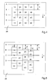
- FIG. 1 The exemplary sketch shown shows the location of a number of light sources to a line of objects.
- the FIG. 1 shows, by way of example and without limitation of generality, seven light sources 12 and one object line 14. For each light source 12, the distance s is the perpendicular from the center 18 of the light source 12 to the object line 14. In most cases, the article line 14 will be substantially parallel to a boundary line of the emitter surface of the light source 12 in which FIG. 1 However, the general case, in which also the distances s of the individual light sources are different in size, shown.
- the FIG. 2 schematically represents a preferred embodiment of the imaging device according to the invention with a time delay device for different circuit of individual light sources.
- the imaging module 10 consists of a single controllable array of a number of light sources 12 typically laser light sources, in particular diode laser arrays.
- the light sources 12 are not located on an object line 14, but each have an individual distance to this object line 14.
- the FIG. 2 By way of example, the general case is shown that not all the light sources 12 lie in a half-plane of the object line, which is bounded by the straight line passing through the object line.
- the light beams 24 emitted by the light sources 12 are imaged onto pixels 210 on a printing form 28 by means of imaging optics 26.
- the pixels 210 to a projection line 16 which corresponds to the imaging of the object line 14 by the imaging optics 26 at a first time, an individual Distance up.
- the distance of a specific pixel 210 to the projection line 16 will be proportional to the distance of the pixel 210 generating light source 12 to the object line 14 with the proportionality factor of the projection ratio k of the imaging optics 26 in the absence of aberrations of the imaging optics.
- the light sources 12 in the imaging module 10 can be used in continuous laser mode. To generate individual light packets, the laser emission is correspondingly suppressed or interrupted for a certain time interval. Since the printing form 28 moves at least tangentially to the surface of the printing plate 28 relative to a speed component v to the imaging device, the pixels 210 of the light sources 12 are at different triggering times at different coordinate positions on the surface of the printing plate 28 when the light sources 12 are all triggered simultaneously The projection line 16 of the object line 14 moves with the printing form 28.
- the imaging optics 26 can have both reflective, transmissive, refractive or similar optical components. Preferably, these are micro-optical components, ie components which influence the light emitted by an individual light source 12, while the light from the other light sources 12 remains unaffected by this component.
- the imaging optics 26 can have both a magnifying and reducing as well as in the two directions parallel and perpendicular to the active zone of the laser different magnifications, which is particularly advantageous for divergence and / or aberration correction.
- the surface of the printing form 28 is changed in its physical and / or chemical properties by the laser radiation, so that image information for a pressure point is written by the exposure with a certain intensity and during a certain time interval.
- the imaging module 10 is located on a cooling element 212, for example, a copper heat sink with cooling water flow.
- the Imaging module 10 is connected to a drive device 216 by means of a line for power supply and control 214.
- the drive device 216 has individual components with which it is possible to control or regulate the individual light sources 12 of the array separately from each other.
- the cooling element 212 is connected to the temperature control 220.
- the embodiment of the imaging device according to the invention which in FIG. 2 is shown comprises a delay device 222, which is integrated in a compact design with the imaging module 10.
- the delay device 222 is linked to the control device 216 via the connection 224, that is to say it is assigned to it.
- the delay device 222 preferably comprises a programmable logic or an ASIC, an application-specific integrated circuit.
- the FIG. 3 shows an embodiment of the imaging device according to the invention with a time delay device for imaging a printing form, which is accommodated on a rotatable cylinder.
- the imaging module 30 has, for example, three light sources, so that three light beams 32 are generated, which are imaged by means of the imaging optics 34 onto three pixels 310 on the printing form 38.
- the three pixels have an individual distance to a projection line 18. Without limiting the generality, a projection line 18 is shown, for which it holds that the three pixels 310 lie in a half plane of the projection plane which is bounded by the straight line passing through the projection line 18.
- the printing form 38 is located on a cylinder 36, which is rotatable about its axis of symmetry 35. This rotation is indicated by the arrow R.
- the imaging module 30 can be moved substantially parallel to the axis of symmetry 35 of the cylinder 36 in substantially linear ways, which is marked with the double arrow T.
- the cylinder 36 rotates with printing form 38 received thereon in accordance with the rotational movement R, and the imaging module 30 translates along the cylinder 36 according to the direction of movement T.
- the result is an illustration which rotates helically about the axis of symmetry 35 of the cylinder 36.
- the path of the projection points or pixels 310 is indicated by the lines 312.
- the imaging module 30 is linked to a connection 314 with a control unit 316.
- the control unit 316 comprises a delay device 318 and a drive device 320.
- FIGS. 4, 5 . 6 and 7 serve to illustrate by way of example without limitation of generality, such as with the imaging device according to the invention with a number of light sources, each having a distance s i , the index i counting the light sources, to an object line in the plane defined by the light sources, to Generation of pixels of the light sources in a projection line of the object line on a printing form, which moves at least with a velocity component v perpendicular to that through the object line and tangent to the surface of the printing form, pressure points generated by pixels on the projection line or a field of pressure points by rows becomes.
- the FIG. 4 is an exemplary sketch for explaining the notation used with respect to the position to be imaged pressure points on a printing form 28.
- the FIG. 4 is based without limitation on the generality of four emitters or light sources, which here for example generate a field of 4 x 4 pressure points through pixels of the light sources on the printing form.
- a regular Cartesian field is to be described.
- other patterns to imprinting pressure points are conceivable.
- the extension of a pressure point or the distance between adjacent pressure points to each other, measured from one center to the next center is designated by h.
- the pressure points are shown as squares; the actual shape is determined by the shape of the imaging light beam with its process parameters such as intensity, exposure time, relative speed between printing form and imaging light beam, and the like.
- the pressure points in the field are denoted by a number-letter combination: The number corresponds to the index, which counts the individual light sources, in particular lasers, while the letter in the order of the alphabet counts the time-sequential imaging steps.
- the FIG. 4 shows a first projection line A, a second projection line B, a third projection line C and a fourth projection line D, which pass the projection points of the four emitters or light sources not shown here in succession, when the printing form with a velocity component v in the arrow direction relative to the light sources moved to a comprehensive imaging module.
- a trigger or switching signal is generated for triggering the imaging by the pixel, so that a pressure point is set.
- FIG. 5 is a schematic representation of an exemplary layer of pixels without compensation on the printing plate 28 shown by the time delay device of the imaging device according to the invention.
- the projection point of the second light source happens to be the first projection line A in time here, without restricting the generality. If all the light sources are driven at the same time, the pixels of the objects are due to the individual distance of each light source to an object line in the plane defined by the light sources shifted from other light sources compared to the starting edge of the pixel 2A or added.
- the pixels generated by the first light source have a first offset L1
- the pixels produced by the third light source have a third offset L3
- the pixels generated by the fourth light source have a fourth offset L4. Is exemplary in the FIG. 5 have shown that the pixels of the fourth light source are more than one pressure point h from the corresponding projection line.
- FIG. 6 is a schematic representation of the exemplary position of pixels without compensation on the printing plate 28 by changing the control of the light sources with those projection points or pixels whose distance is greater than the pressure point distance.
- position deviations greater than two pixel lengths h are compensated for by temporally shifting the data in accordance with two imaging steps. By means of this procedure of shifting data, it can be achieved that all position deviations are smaller than one pixel length h.
- Exemplary is in FIG. 6 the distance of the fourth pixel to the fourth residual offset L4 'is reduced, in other words L4' in this case corresponds to the remainder of the division (L4 mod h).
- the FIG. 7 is a schematic representation of the position of pixels with compensation by delayed control of the light sources after a triggering time of a temporally considered first light source, here for example the second light source.
- the data transfer and the triggering of the light sources after a triggering time of a first light source light sources can be delayed.
- the desired field of pressure points will be generated by iteration for each additional projection line, as described in the following FIG. 4 is shown generated.
- the delay device should be operated at a signal frequency that is a multiple of the frequency of the original drive signal.
- the realization of the displacement by delayed activation is effected by the delay device, which has, for example, a programmable logic, an ASIC, a discrete electronics or the like.
- the delay electronics are provided with the distances s i , the index i counting the light sources, and the projection ratio k between the object line and the projection line in a suitable form, for example by storage in a memory unit.
- the deceleration device can determine from these indications, the velocity component v of the relative movement between the printing form and the imaging device with a known velocity profile of the printing form, for example a uniform movement, starting values for counters, which are each assigned to a light source. At a fixed clock frequency of the delay device elapses depending on the counter start a certain time interval, was counted down to zero, so that a delayed triggering of the control of the corresponding light source can be triggered upon reaching the zero value of the counter.
- the distances s i can be determined as part of a calibration or measurement for an object line in the object plane. It is clear in this context that the distances s i of the light sources can be converted to a first object line with simple arithmetic at distances to a second object line.
Landscapes
- Engineering & Computer Science (AREA)
- Toxicology (AREA)
- Physics & Mathematics (AREA)
- Optics & Photonics (AREA)
- Health & Medical Sciences (AREA)
- General Health & Medical Sciences (AREA)
- Manufacturing & Machinery (AREA)
- Multimedia (AREA)
- Signal Processing (AREA)
- Exposure And Positioning Against Photoresist Photosensitive Materials (AREA)
- Manufacture Or Reproduction Of Printing Formes (AREA)
- Printers Or Recording Devices Using Electromagnetic And Radiation Means (AREA)
- Editing Of Facsimile Originals (AREA)
- Studio Devices (AREA)
Applications Claiming Priority (2)
| Application Number | Priority Date | Filing Date | Title |
|---|---|---|---|
| DE10124215A DE10124215A1 (de) | 2001-05-18 | 2001-05-18 | Bebilderungseinrichtung zur Erzeugung einer Anzahl von Bildpunkten in einer Projektionslinie |
| DE10124215 | 2001-05-18 |
Publications (3)
| Publication Number | Publication Date |
|---|---|
| EP1259060A2 EP1259060A2 (de) | 2002-11-20 |
| EP1259060A3 EP1259060A3 (de) | 2005-05-18 |
| EP1259060B1 true EP1259060B1 (de) | 2012-03-07 |
Family
ID=7685246
Family Applications (1)
| Application Number | Title | Priority Date | Filing Date |
|---|---|---|---|
| EP02009280A Expired - Lifetime EP1259060B1 (de) | 2001-05-18 | 2002-04-29 | Bebilderungseinrichtung zur Erzeugung einer Anzahl von Bildpunkten in einer Projektionslinie |
Country Status (9)
Families Citing this family (4)
| Publication number | Priority date | Publication date | Assignee | Title |
|---|---|---|---|---|
| JP4505250B2 (ja) | 2003-06-16 | 2010-07-21 | ハイデルベルガー ドルツクマシーネン アクチエンゲゼルシヤフト | 版のための描画装置および光学要素を描画装置に配置する方法 |
| JP5095946B2 (ja) * | 2005-02-18 | 2012-12-12 | ハイデルベルガー ドルツクマシーネン アクチエンゲゼルシヤフト | 少なくとも1つのレーザダイオードバーを備える版の画像付け装置 |
| DE202008004285U1 (de) | 2008-03-28 | 2008-07-03 | Man Roland Druckmaschinen Ag | Bebilderungseinrichtung |
| DE102013102599A1 (de) * | 2013-03-14 | 2014-09-18 | Limo Patentverwaltung Gmbh & Co. Kg | Beleuchtungsvorrichtung |
Family Cites Families (24)
| Publication number | Priority date | Publication date | Assignee | Title |
|---|---|---|---|---|
| DE2653539C3 (de) | 1976-11-25 | 1979-10-04 | Dr.-Ing. Rudolf Hell Gmbh, 2300 Kiel | Anordnung zur Aufzeichnung von gerasterten Halbtonbildern |
| JPS6031417B2 (ja) * | 1980-01-30 | 1985-07-22 | 沖電気工業株式会社 | 光走査装置 |
| DE3376727D1 (en) * | 1983-11-01 | 1988-06-23 | Agfa Gevaert Nv | Recording apparatus |
| US5163368B1 (en) | 1988-08-19 | 1999-08-24 | Presstek Inc | Printing apparatus with image error correction and ink regulation control |
| US5174205B1 (en) | 1991-01-09 | 1999-10-05 | Presstek Inc | Controller for spark discharge imaging |
| DE9219213U1 (de) * | 1991-01-09 | 2000-08-03 | Presstek, Inc., Hudson, N.H. | Steuerungsgerät für Funkenentladungsbilderzeugung |
| US5274394A (en) * | 1991-05-22 | 1993-12-28 | Xerox Corporation | Electronic adjustment of slow scan image registration in an image recording apparatus |
| US5379698A (en) * | 1992-07-20 | 1995-01-10 | Presstek, Inc. | Lithographic printing members for use with laser-discharge imaging |
| DE9302494U1 (de) * | 1993-02-20 | 1993-04-22 | Man Roland Druckmaschinen Ag, 63069 Offenbach | Anordnung zum Bebildern einer Schicht auf der Oberfläche eines Formzylinders |
| JPH07333938A (ja) * | 1994-06-09 | 1995-12-22 | Canon Inc | カラ−画像形成装置 |
| DE19602307A1 (de) * | 1996-01-23 | 1997-07-24 | Roland Man Druckmasch | Druckmaschine |
| US5854651A (en) * | 1996-05-31 | 1998-12-29 | Eastman Kodak Company | Optically correcting deviations from straightness of laser emitter arrays |
| US5900981A (en) | 1997-04-15 | 1999-05-04 | Scitex Corporation Ltd. | Optical system for illuminating a spatial light modulator |
| US6141030A (en) | 1997-04-24 | 2000-10-31 | Konica Corporation | Laser exposure unit including plural laser beam sources differing in wavelength |
| US6091891A (en) * | 1997-05-09 | 2000-07-18 | Lexmark International, Inc. | Method and apparatus for calibrating delay lines to create gray levels in continuous tone printing |
| JP3381582B2 (ja) * | 1997-06-27 | 2003-03-04 | カシオ電子工業株式会社 | 光書き込みヘッド駆動装置、及びその装置を使用する光書き込みヘッド駆動方法 |
| JPH1110949A (ja) * | 1997-06-27 | 1999-01-19 | Ricoh Co Ltd | マルチビーム画像形成装置 |
| US6044096A (en) | 1997-11-03 | 2000-03-28 | Sdl, Inc. | Packaged laser diode array system and method with reduced asymmetry |
| JPH11138898A (ja) * | 1997-11-11 | 1999-05-25 | Fuji Photo Film Co Ltd | 露光装置及び露光方法 |
| DE60027059T2 (de) * | 1999-01-18 | 2007-03-15 | Fuji Photo Film Co., Ltd., Minami-Ashigara | Flachdruck-Verfahren und -Vorrichtung |
| US6390579B1 (en) * | 1999-04-15 | 2002-05-21 | Hewlett-Packard Company | Pulse width modulator using delay-line technology with automatic calibration of delays to desired operating frequency |
| US6532029B1 (en) * | 2000-11-21 | 2003-03-11 | Aetas Technology Incorporated | Imaging-offset compensation methods and systems |
| US6603498B1 (en) * | 2000-11-28 | 2003-08-05 | Coherent, Inc. | Printer head with linear array of individually addressable diode-lasers |
| US6819351B2 (en) * | 2001-05-30 | 2004-11-16 | Nexpress Solutions Llc | Coarse and fine electronic bow correction for a writer |
-
2001
- 2001-05-18 DE DE10124215A patent/DE10124215A1/de not_active Ceased
-
2002
- 2002-03-28 CZ CZ20021103A patent/CZ20021103A3/cs unknown
- 2002-04-09 CA CA002380985A patent/CA2380985A1/en not_active Abandoned
- 2002-04-29 AT AT02009280T patent/ATE548196T1/de active
- 2002-04-29 EP EP02009280A patent/EP1259060B1/de not_active Expired - Lifetime
- 2002-05-13 IL IL14961502A patent/IL149615A0/xx not_active IP Right Cessation
- 2002-05-15 US US10/146,245 patent/US7843480B2/en not_active Expired - Fee Related
- 2002-05-17 JP JP2002142924A patent/JP2003035958A/ja active Pending
- 2002-05-17 CN CN02120274.5A patent/CN1268983C/zh not_active Expired - Fee Related
Also Published As
| Publication number | Publication date |
|---|---|
| EP1259060A2 (de) | 2002-11-20 |
| ATE548196T1 (de) | 2012-03-15 |
| DE10124215A1 (de) | 2002-11-21 |
| IL149615A0 (en) | 2002-11-10 |
| CZ20021103A3 (cs) | 2003-01-15 |
| US20030026176A1 (en) | 2003-02-06 |
| CA2380985A1 (en) | 2002-11-18 |
| CN1386635A (zh) | 2002-12-25 |
| CN1268983C (zh) | 2006-08-09 |
| EP1259060A3 (de) | 2005-05-18 |
| US7843480B2 (en) | 2010-11-30 |
| HK1051837A1 (en) | 2003-08-22 |
| JP2003035958A (ja) | 2003-02-07 |
Similar Documents
| Publication | Publication Date | Title |
|---|---|---|
| EP1168813B1 (de) | Kompakte Mehrstrahllaserlichtquelle und Interleafrasterscanlinien-Verfahren zur Belichtung von Druckplatten | |
| EP0907906B1 (de) | Lithographie-belichtungseinrichtung | |
| EP1241013B1 (de) | Bebilderungseinrichtung für eine Druckform mit einem Array von VCSEL-Lichtquellen | |
| DE69217324T2 (de) | Laser-Markierungsvorrichtung mit verbesserter Druckqualität | |
| DE69125631T2 (de) | Vorrichtung zum punktrasterschreiben mittels eines dauerstrichlasers | |
| EP3538350A1 (de) | Vorrichtung und verfahren zur generativen bauteilfertigung mit mehreren räumlich getrennten strahlführungen | |
| DE3427611A1 (de) | Laserstrahl-lithograph | |
| EP1235111A2 (de) | Banding-reduzierende Bebilderung einer Druckform | |
| WO2017162647A1 (de) | Vorrichtung und verfahren zur erzeugung eines optischen musters aus bildpunkten in einer bildebene | |
| DE102020201161A1 (de) | Vorrichtung, Lasersystem und Verfahren zur Kombination von kohärenten Laserstrahlen | |
| DE102018205270A1 (de) | Laserstrahlpositioniersystem, Laserbearbeitungsvorrichtung und Steuerungsverfahren | |
| EP1617275A1 (de) | Vorrichtung für die Beleuchtung einer Fläche mit einem Halbleiterlaserbarren und Strahltransformationsmitteln | |
| DE102020200444A1 (de) | Vorrichtung, Lasersystem und Verfahren zur Kombination von kohärenten Laserstrahlen | |
| DE69921739T2 (de) | Bildaufzeichnungsgerät | |
| EP1278611B1 (de) | Vorrichtung zur beschriftung von gegenständen mittels laserstrahlen | |
| DE60102597T2 (de) | Laser mit hoher spitzenleistung und dessen anwendung zur erzeugung von licht im extrem-uv-bereich | |
| EP3559724B1 (de) | Vorrichtung und verfahren zur belichtung einer lichtempfindlichen schicht | |
| EP1259060B1 (de) | Bebilderungseinrichtung zur Erzeugung einer Anzahl von Bildpunkten in einer Projektionslinie | |
| WO2000011513A1 (de) | Vorrichtung zur volumetrischen wiedergabe eines dreidimensionalen bildes durch gepulste plasmaerzeugung in natürlicher atmosphäre mittels eines fokussierten laserstrahls | |
| DE2822639C2 (de) | Einrichtung zur Mehrfachbelichtung einzelner Bildpunkte | |
| DE10233491B4 (de) | Kompakte Einrichtung zur Bebilderung einer Druckform | |
| DE10239003A1 (de) | Mehrstrahllaserlichtquelle mit variablem Laserlichtquellenabstand zur Bebilderung von Druckformen | |
| DE102013212363A1 (de) | Facettenspiegel, insbesondere für die EUV-Projektionslithografie | |
| EP2356518B1 (de) | Verfahren und vorrichtung zur bebilderung eines strahlungsempfindlichen substrats | |
| DE102020200348A1 (de) | LiDAR System |
Legal Events
| Date | Code | Title | Description |
|---|---|---|---|
| PUAI | Public reference made under article 153(3) epc to a published international application that has entered the european phase |
Free format text: ORIGINAL CODE: 0009012 |
|
| AK | Designated contracting states |
Kind code of ref document: A2 Designated state(s): AT BE CH CY DE DK ES FI FR GB GR IE IT LI LU MC NL PT SE TR |
|
| AX | Request for extension of the european patent |
Free format text: AL;LT;LV;MK;RO;SI |
|
| PUAL | Search report despatched |
Free format text: ORIGINAL CODE: 0009013 |
|
| AK | Designated contracting states |
Kind code of ref document: A3 Designated state(s): AT BE CH CY DE DK ES FI FR GB GR IE IT LI LU MC NL PT SE TR |
|
| AX | Request for extension of the european patent |
Extension state: AL LT LV MK RO SI |
|
| RIC1 | Information provided on ipc code assigned before grant |
Ipc: 7B 41J 2/45 B Ipc: 7H 04N 1/053 A |
|
| 17P | Request for examination filed |
Effective date: 20050420 |
|
| AKX | Designation fees paid |
Designated state(s): AT BE CH CY DE DK ES FI FR GB GR IE IT LI LU MC NL PT SE TR |
|
| 17Q | First examination report despatched |
Effective date: 20050829 |
|
| GRAP | Despatch of communication of intention to grant a patent |
Free format text: ORIGINAL CODE: EPIDOSNIGR1 |
|
| RIC1 | Information provided on ipc code assigned before grant |
Ipc: B41J 2/45 20060101AFI20110914BHEP Ipc: H04N 1/053 20060101ALI20110914BHEP |
|
| GRAS | Grant fee paid |
Free format text: ORIGINAL CODE: EPIDOSNIGR3 |
|
| GRAA | (expected) grant |
Free format text: ORIGINAL CODE: 0009210 |
|
| AK | Designated contracting states |
Kind code of ref document: B1 Designated state(s): AT BE CH CY DE DK ES FI FR GB GR IE IT LI LU MC NL PT SE TR |
|
| REG | Reference to a national code |
Ref country code: GB Ref legal event code: FG4D Free format text: NOT ENGLISH |
|
| REG | Reference to a national code |
Ref country code: AT Ref legal event code: REF Ref document number: 548196 Country of ref document: AT Kind code of ref document: T Effective date: 20120315 Ref country code: CH Ref legal event code: EP |
|
| REG | Reference to a national code |
Ref country code: IE Ref legal event code: FG4D Free format text: LANGUAGE OF EP DOCUMENT: GERMAN |
|
| REG | Reference to a national code |
Ref country code: NL Ref legal event code: T3 |
|
| REG | Reference to a national code |
Ref country code: DE Ref legal event code: R096 Ref document number: 50215404 Country of ref document: DE Effective date: 20120503 |
|
| PG25 | Lapsed in a contracting state [announced via postgrant information from national office to epo] |
Ref country code: FI Free format text: LAPSE BECAUSE OF FAILURE TO SUBMIT A TRANSLATION OF THE DESCRIPTION OR TO PAY THE FEE WITHIN THE PRESCRIBED TIME-LIMIT Effective date: 20120307 Ref country code: GR Free format text: LAPSE BECAUSE OF FAILURE TO SUBMIT A TRANSLATION OF THE DESCRIPTION OR TO PAY THE FEE WITHIN THE PRESCRIBED TIME-LIMIT Effective date: 20120608 |
|
| PG25 | Lapsed in a contracting state [announced via postgrant information from national office to epo] |
Ref country code: CY Free format text: LAPSE BECAUSE OF FAILURE TO SUBMIT A TRANSLATION OF THE DESCRIPTION OR TO PAY THE FEE WITHIN THE PRESCRIBED TIME-LIMIT Effective date: 20120307 |
|
| BERE | Be: lapsed |
Owner name: HEIDELBERGER DRUCKMASCHINEN A.G. Effective date: 20120430 |
|
| PG25 | Lapsed in a contracting state [announced via postgrant information from national office to epo] |
Ref country code: SE Free format text: LAPSE BECAUSE OF FAILURE TO SUBMIT A TRANSLATION OF THE DESCRIPTION OR TO PAY THE FEE WITHIN THE PRESCRIBED TIME-LIMIT Effective date: 20120307 |
|
| PG25 | Lapsed in a contracting state [announced via postgrant information from national office to epo] |
Ref country code: MC Free format text: LAPSE BECAUSE OF NON-PAYMENT OF DUE FEES Effective date: 20120430 Ref country code: PT Free format text: LAPSE BECAUSE OF FAILURE TO SUBMIT A TRANSLATION OF THE DESCRIPTION OR TO PAY THE FEE WITHIN THE PRESCRIBED TIME-LIMIT Effective date: 20120709 |
|
| REG | Reference to a national code |
Ref country code: CH Ref legal event code: PL |
|
| PLBE | No opposition filed within time limit |
Free format text: ORIGINAL CODE: 0009261 |
|
| STAA | Information on the status of an ep patent application or granted ep patent |
Free format text: STATUS: NO OPPOSITION FILED WITHIN TIME LIMIT |
|
| PG25 | Lapsed in a contracting state [announced via postgrant information from national office to epo] |
Ref country code: LI Free format text: LAPSE BECAUSE OF NON-PAYMENT OF DUE FEES Effective date: 20120430 Ref country code: DK Free format text: LAPSE BECAUSE OF FAILURE TO SUBMIT A TRANSLATION OF THE DESCRIPTION OR TO PAY THE FEE WITHIN THE PRESCRIBED TIME-LIMIT Effective date: 20120307 Ref country code: CH Free format text: LAPSE BECAUSE OF NON-PAYMENT OF DUE FEES Effective date: 20120430 Ref country code: BE Free format text: LAPSE BECAUSE OF NON-PAYMENT OF DUE FEES Effective date: 20120430 |
|
| 26N | No opposition filed |
Effective date: 20121210 |
|
| GBPC | Gb: european patent ceased through non-payment of renewal fee |
Effective date: 20120607 |
|
| REG | Reference to a national code |
Ref country code: DE Ref legal event code: R097 Ref document number: 50215404 Country of ref document: DE Effective date: 20121210 |
|
| PG25 | Lapsed in a contracting state [announced via postgrant information from national office to epo] |
Ref country code: ES Free format text: LAPSE BECAUSE OF FAILURE TO SUBMIT A TRANSLATION OF THE DESCRIPTION OR TO PAY THE FEE WITHIN THE PRESCRIBED TIME-LIMIT Effective date: 20120618 Ref country code: IE Free format text: LAPSE BECAUSE OF NON-PAYMENT OF DUE FEES Effective date: 20120429 Ref country code: GB Free format text: LAPSE BECAUSE OF NON-PAYMENT OF DUE FEES Effective date: 20120607 |
|
| REG | Reference to a national code |
Ref country code: AT Ref legal event code: MM01 Ref document number: 548196 Country of ref document: AT Kind code of ref document: T Effective date: 20120429 |
|
| PG25 | Lapsed in a contracting state [announced via postgrant information from national office to epo] |
Ref country code: AT Free format text: LAPSE BECAUSE OF NON-PAYMENT OF DUE FEES Effective date: 20120429 |
|
| PGFP | Annual fee paid to national office [announced via postgrant information from national office to epo] |
Ref country code: NL Payment date: 20130427 Year of fee payment: 12 |
|
| PG25 | Lapsed in a contracting state [announced via postgrant information from national office to epo] |
Ref country code: TR Free format text: LAPSE BECAUSE OF FAILURE TO SUBMIT A TRANSLATION OF THE DESCRIPTION OR TO PAY THE FEE WITHIN THE PRESCRIBED TIME-LIMIT Effective date: 20120307 |
|
| PG25 | Lapsed in a contracting state [announced via postgrant information from national office to epo] |
Ref country code: LU Free format text: LAPSE BECAUSE OF NON-PAYMENT OF DUE FEES Effective date: 20120429 |
|
| PGFP | Annual fee paid to national office [announced via postgrant information from national office to epo] |
Ref country code: FR Payment date: 20140424 Year of fee payment: 13 Ref country code: IT Payment date: 20140419 Year of fee payment: 13 Ref country code: DE Payment date: 20140430 Year of fee payment: 13 |
|
| REG | Reference to a national code |
Ref country code: NL Ref legal event code: V1 Effective date: 20141101 |
|
| PG25 | Lapsed in a contracting state [announced via postgrant information from national office to epo] |
Ref country code: NL Free format text: LAPSE BECAUSE OF NON-PAYMENT OF DUE FEES Effective date: 20141101 |
|
| REG | Reference to a national code |
Ref country code: DE Ref legal event code: R119 Ref document number: 50215404 Country of ref document: DE |
|
| PG25 | Lapsed in a contracting state [announced via postgrant information from national office to epo] |
Ref country code: DE Free format text: LAPSE BECAUSE OF NON-PAYMENT OF DUE FEES Effective date: 20151103 Ref country code: IT Free format text: LAPSE BECAUSE OF NON-PAYMENT OF DUE FEES Effective date: 20150429 |
|
| REG | Reference to a national code |
Ref country code: FR Ref legal event code: ST Effective date: 20151231 |
|
| PG25 | Lapsed in a contracting state [announced via postgrant information from national office to epo] |
Ref country code: FR Free format text: LAPSE BECAUSE OF NON-PAYMENT OF DUE FEES Effective date: 20150430 |