EP1258906A1 - Image display device, method of manufacture thereof, and apparatus for charging sealing material - Google Patents
Image display device, method of manufacture thereof, and apparatus for charging sealing material Download PDFInfo
- Publication number
- EP1258906A1 EP1258906A1 EP01901516A EP01901516A EP1258906A1 EP 1258906 A1 EP1258906 A1 EP 1258906A1 EP 01901516 A EP01901516 A EP 01901516A EP 01901516 A EP01901516 A EP 01901516A EP 1258906 A1 EP1258906 A1 EP 1258906A1
- Authority
- EP
- European Patent Office
- Prior art keywords
- sealing material
- metal sealing
- image display
- display apparatus
- rear substrate
- Prior art date
- Legal status (The legal status is an assumption and is not a legal conclusion. Google has not performed a legal analysis and makes no representation as to the accuracy of the status listed.)
- Withdrawn
Links
Images




Classifications
-
- H—ELECTRICITY
- H01—ELECTRIC ELEMENTS
- H01J—ELECTRIC DISCHARGE TUBES OR DISCHARGE LAMPS
- H01J1/00—Details of electrodes, of magnetic control means, of screens, or of the mounting or spacing thereof, common to two or more basic types of discharge tubes or lamps
- H01J1/02—Main electrodes
- H01J1/30—Cold cathodes, e.g. field-emissive cathode
-
- H—ELECTRICITY
- H01—ELECTRIC ELEMENTS
- H01J—ELECTRIC DISCHARGE TUBES OR DISCHARGE LAMPS
- H01J31/00—Cathode ray tubes; Electron beam tubes
- H01J31/08—Cathode ray tubes; Electron beam tubes having a screen on or from which an image or pattern is formed, picked up, converted, or stored
- H01J31/10—Image or pattern display tubes, i.e. having electrical input and optical output; Flying-spot tubes for scanning purposes
- H01J31/12—Image or pattern display tubes, i.e. having electrical input and optical output; Flying-spot tubes for scanning purposes with luminescent screen
- H01J31/123—Flat display tubes
- H01J31/125—Flat display tubes provided with control means permitting the electron beam to reach selected parts of the screen, e.g. digital selection
- H01J31/127—Flat display tubes provided with control means permitting the electron beam to reach selected parts of the screen, e.g. digital selection using large area or array sources, i.e. essentially a source for each pixel group
-
- H—ELECTRICITY
- H01—ELECTRIC ELEMENTS
- H01J—ELECTRIC DISCHARGE TUBES OR DISCHARGE LAMPS
- H01J9/00—Apparatus or processes specially adapted for the manufacture, installation, removal, maintenance of electric discharge tubes, discharge lamps, or parts thereof; Recovery of material from discharge tubes or lamps
- H01J9/24—Manufacture or joining of vessels, leading-in conductors or bases
- H01J9/26—Sealing together parts of vessels
- H01J9/261—Sealing together parts of vessels the vessel being for a flat panel display
-
- H—ELECTRICITY
- H01—ELECTRIC ELEMENTS
- H01J—ELECTRIC DISCHARGE TUBES OR DISCHARGE LAMPS
- H01J2209/00—Apparatus and processes for manufacture of discharge tubes
- H01J2209/26—Sealing parts of the vessel to provide a vacuum enclosure
- H01J2209/261—Apparatus used for sealing vessels, e.g. furnaces, machines or the like
- H01J2209/262—Apparatus used for sealing vessels, e.g. furnaces, machines or the like means for applying sealing materials, e.g. frit paste dispensers
-
- H—ELECTRICITY
- H01—ELECTRIC ELEMENTS
- H01J—ELECTRIC DISCHARGE TUBES OR DISCHARGE LAMPS
- H01J2209/00—Apparatus and processes for manufacture of discharge tubes
- H01J2209/26—Sealing parts of the vessel to provide a vacuum enclosure
- H01J2209/264—Materials for sealing vessels, e.g. frit glass compounds, resins or structures
-
- H—ELECTRICITY
- H01—ELECTRIC ELEMENTS
- H01J—ELECTRIC DISCHARGE TUBES OR DISCHARGE LAMPS
- H01J2329/00—Electron emission display panels, e.g. field emission display panels
- H01J2329/86—Vessels
- H01J2329/867—Seals between parts of vessels
- H01J2329/8675—Seals between the frame and the front and/or back plate
Definitions
- the present invention relates to a flat, planar-type image display apparatus comprising an evacuated envelope, a method of manufacturing the image display apparatus, and a sealing-material applying apparatus.
- display apparatuses have been developed as next- generation, lightweight, thin, planar-type displays. These apparatus comprise a phosphor screen and a number of electron-emitting elements (hereinafter called “emitters”). The emitters are arranged, opposing the phosphor screen. The emitters may be of either field emission type or surface conduction type. Display apparatuses using field emission type electron-emitting elements as emitters are generally called “field emission displays” (hereinafter referred to as “FEDs”). Display apparatuses using surface conduction type electron-emitting elements as emitters are generally called “surface conduction type electronic discharge display” (hereinafter referred to as "SEDs").
- FEDs field emission displays
- SEDs surface conduction type electronic discharge display
- FEDs generally have a front substrate and a rear substrate opposing each other and spaced apart by a predetermined distance. These substrates constitute an evacuated envelope, because they are coupled together at their circumferential edges, with a rectangle frame-like sidewall interposed between them.
- the phosphor screen is formed on the inner surface of the front substrate.
- a number of emitters are provided on the inner surface of the rear substrate. The emitters are used as electron-emitting sources. The electrons they emit excite phosphor layers, causing the phosphor layers to emit light.
- a plurality of support members are interposed between the front substrate and the rear substrate to withstand atmospheric pressure applied on these substrates.
- the electric potential at the rear substrate is about 0V.
- the anode voltage Va is applied to the phosphor screen.
- the electron beams emitted from the emitters are applied to the red phosphor layers, that constitute the phosphor screen, to energize the phosphor layers, whereby an image is displayed.
- the distance between the front substrate and the rear substrate can be set at several millimeters or less. Therefore, FED is lighter and thinner than the cathode-ray tube (CRT) used at present as a display of televisions or computers.
- CTR cathode-ray tube
- the surface adsorption gas inside the envelope is liberated by performing baking in which the envelope is heated to about 300°C.
- the evacuation method cannot completely liberate the surface adsorption gas.
- Jpn. Pat. Appln. KOKAI Publication No. 9-82245 discloses a planar display apparatuses of various structures.
- getter material such as Ti, Zr or alloy thereof covers the metal back that is formed on the phosphor screen of the front substrate.
- the metal back is made of getter material.
- getter material covers the components other than the electron-emitting elements, in the image-displaying region.
- getter material is formed in the ordinary panel process. Inevitably, the surface of getter material will be oxidized. The getter material is highly active at the surface. Once oxidized at surface, the getter material can no longer adsorb gas as much as desired.
- a method of enhancing the degree of vacuum inside the evacuated envelope may be considered.
- a rear substrate, a sidewall, and a front substrate are brought into a vacuum chamber. These components are baked in the vacuum atmosphere and irradiated with an electron beam. The surface adsorption gas is thereby released from the rear substrate, sidewall and front substrate. Thereafter, a getter film is formed, and the sidewall, rear substrate and front substrate are sealed together, with frit glass or the like, in the vacuum atmosphere.
- This method can release the surface adsorption gas sufficiently by means of electron-beam washing. The getter film is not oxidized. A sufficient gas adsorption can be accomplished. In addition, the space in the image display apparatus is not wasted because no evacuation pipes are necessary.
- the frit glass must be heated to a high temperature of 400°C or more. When so heated, the frit glass generates air bubbles. This degrades the air-tightness, sealing strength and the like of the evacuated envelope. Consequently, the reliability of the image display apparatus decreases. In view of the characteristic of the electron-emitting elements, it may be desirable not to heat the frit glass to 400°C or more. In such a case, the method of sealing the components with frit glass is not desirable.
- An object of the invention is to provide an image display apparatus comprising an envelope which can be easily sealed and which can maintain a high vacuum, to provide a method of manufacturing the image display apparatus, and to provide a sealing-material applying apparatus.
- an image display apparatus comprises an envelope having a rear substrate, a front substrate opposing the rear substrate, and a number of electron-emitting elements provided in the envelope.
- the front substrate and the rear substrate are sealed, at edge parts, either directly or indirectly to each other with low melting-point metal sealing material.
- the low melting-point metal sealing material preferably have a melting point of 350°C or less. Further, it is desired that the low melting-point metal sealing material be indium or an alloy containing indium.
- a method of manufacturing an image display apparatus which comprises an envelope having a rear substrate, a front substrate opposing the rear substrate, and a number of electron-emitting elements provided in the envelope.
- the method comprises the steps of: applying low melting-point metal sealing material to a sealing surface lying between the rear substrate and the front substrate; and sealing the rear substrate and the front substrate together, either directly or indirectly to each other, by heating the rear substrate and the front substrate in a vacuum atmosphere and by melting the low melting-point metal sealing material.
- the low melting-point metal sealing material In the method of manufacturing an image display apparatus, it is preferred that the low melting-point metal sealing material have a melting point of 350°C or less. Moreover, it is desired that the low melting-point metal sealing material be indium or an alloy containing indium.
- the degree of vacuum in the envelope is preferably 10 -3 Pa or less.
- the sealing the rear substrate and the front substrate together includes an evacuating step of heating the vacuum atmosphere to a temperature of 250°C or more; a sealing step of sealing the front substrate and the rear substrate by applying the low melting-point metal sealing material to a sealing surface lying between the front and rear substrates, at a temperature lower than the temperature used in the evacuating step; and a step of bringing the envelope sealed with the low melting-point metal sealing material, back into the atmosphere.
- the sealing may be performed by using the low melting-point metal sealing material at a temperature of 60 to 300°C.
- the front and rear substrates are moved relative to each other and are sealed to each other after low melting-point metal sealing material is applied to sealing surfaces lying between the front substrate and the rear substrate.
- the direction in which the rear plate and the front substrate are moved relative to each other may be any direction in a three-dimensional space, so long as the substrates approach each other. Only one of the substrates may be moved, or both substrates may be moved.
- a material-retaining section is provided to retain the low melting-point metal sealing material, at least of the sealing surfaces lying between the front substrate and the rear substrate.
- the low melting-point metal sealing material is applied onto the material-retaining section.
- the material-retaining section is preferably a groove formed in the sealing surface or a layer formed on the sealing surface and made of material that exhibits high affinity with the low melting-point metal sealing material.
- the material exhibiting high affinity with the low melting-point metal sealing material is preferably nickel, gold, silver or copper, or an alloy thereof.
- the. front and rear substrates forming an envelope can be sealed together in a vacuum atmosphere, by using low melting-point metal sealing material. They are sealed at a low temperature (about 300°C or less) that does no thermal damages to the electron-emitting elements and the like. Any components required in the conventional method, such as thin evacuation pipes, are unnecessary, and the evacuation efficiency can be very high.
- the invention can provide image display apparatuses that have an envelope maintaining a high degree of vacuum and are free of an image-quality decrease due to thermal deterioration of the electron-emitting elements.
- An image display apparatus comprises an envelope having a rear substrate, a front substrate opposing the rear substrate, and a plurality of electron-emitting elements provided in the envelope.
- the front substrate and the rear substrate are sealed either directly or indirectly to each other with a base layer and a metal sealing material layer provided on the base layer and different in material from the base layer.
- An image display apparatus comprises an envelope having a rear substrate, a front substrate opposing the rear substrate and a sidewall arranged between edges of the front substrate and edges of the rear substrate, and a plurality of electron-emitting elements provided on an inner surface of the rear substrate and configured to emit electron beams.
- the front substrate and the sidewall, or the rear substrate and the sidewall, or the front substrate and the side wall and the rear substrate and the side wall are sealed together with a base layer and a metal sealing material layer different in material from a material of the base layer.
- the metal sealing material layer is made of low melting-point metal sealing material having a melting point of 350°C or less.
- the low melting-point metal sealing material may be indium or an alloy containing indium.
- the base layer is made of metal paste containing at least one element selected from the group consisting of silver, gold, aluminum, nickel, cobalt and copper.
- the base layer may be a plated layer or deposited layer made of at least one element selected from the group consisting of silver, gold, aluminum, nickel, cobalt and copper. Still alternatively, it may be made of glass material or the like.
- the front substrate and the rear substrate are sealed with metal sealing material, either directly or indirectly to each other. Therefore, the substrates can be sealed together at a low temperature that does no thermal damages to the electron-emitting elements or the like. A number of bubbles will not develop as in the case where frit glass or the like is used. This helps to improve the air-tightness and sealing strength of the envelope.
- the base layer which is different in material from the metal sealing material layer, prevents the metal sealing material from flowing, thus retaining the material at a predetermined position, even when the metal sealing material melted to have its viscosity reduced.
- the invention can provide an image display apparatus and a method of manufacturing the same, in which the metal sealing material can easily be treated and the sealing step can be performed in a vacuum atmosphere easily and reliably.
- a method of manufacturing an image display apparatus which comprises an envelope having a rear substrate, a front substrate opposing the rear substrate, and a plurality of electron-emitting elements provided in the envelope.
- This method comprises applying molten metal sealing material to a sealing surface lying between the rear substrate and the front substrate, while applying ultrasonic waves; and heating and melting the metal sealing material in a vacuum atmosphere after the metal sealing material has been-applied, and sealing the rear substrate and the front substrate at the sealing surface, either directly or indirectly to each other.
- an image display apparatus which comprises an envelope having a rear substrate, a front substrate opposing the rear substrate, a sidewall arranged between edges of the front substrate and edges of the rear substrate; and a plurality of electron-emitting elements provided in the envelope, wherein the front substrate and the sidewall, or the rear substrate and the sidewall, or the front substrate and the side wall and the rear substrate and sidewall are sealed together with a metal sealing material layer.
- the method comprises the steps of: applying molten metal sealing material to a sealing surface lying between the rear substrate and the front substrate, while applying ultrasonic waves; and heating and melting the metal sealing material in a vacuum atmosphere after the metal sealing material has been applied, and sealing the rear substrate, the front substrate and the sidewall together at the sealing surface.
- the step of applying the metal sealing material includes a step of continuously applying the molten metal sealing material along the sealing surface, thereby forming a metal sealing material layer that extends along the sealing surface.
- the method of manufacturing an image display. apparatus may comprise a step of forming a base layer on the sealing surface.
- the base layer is different in material from the metal sealing material layer.
- the metal sealing material is applied onto the base layer after the base layer has been formed.
- the metal sealing material may be low melting-point metal sealing material that has a melting point of 350°C or less.
- the material is, for example, indium or an alloy containing indium.
- the base layer is made of material that exhibits good wettability and air-tightness with respect to the metal sealing material. In other words, it should be made of material exhibiting high affinity with the metal sealing material.
- the base layer may be made by applying metal paste containing at least one element selected from the group consisting of silver, gold, aluminum, nickel, cobalt, copper nickel, gold, silver and copper. Alternatively, it may be a plated layer or deposited layer made of at least one element selected from the group consisting of silver, gold, aluminum, nickel, cobalt and copper, or is a glass material layer.
- the front substrate and the rear substrate are sealed by using a metal sealing material layer, either directly or indirectly to each other.
- the substrates can therefore be sealed together at such a low temperature as would not do thermal damages to the electron-emitting elements and the like provided on the rear substrate. Further, a number of bubbles will not develop as in the case where frit glass or the like is used. This helps to improve the air-tightness and sealing strength of the envelope.
- the metal sealing material has its wettability to the sealing surface improved, because ultrasonic waves are applied while the metal sealing material is being applied to the sealing surface. Thus, the metal sealing material can remain at a desired position even if it is indium or the like.
- the present invention can provide a method of manufacturing an image display apparatus, in which the components can be sealed together in a vacuum atmosphere, both easily and reliably.
- the molten metal sealing material may be continuously applied along the sealing surface, while ultrasonic waves are being applied.
- the material can form a metal sealing material layer that extends along the sealing surface, without breaks.
- the sealing step can be performed in a vacuum atmosphere, both easily and reliably. In particular, a part of the metal sealing material diffuses into the base layer, forming an alloy layer, when the material is applied while ultrasonic waves are being applied. This more reliably prevents the metal sealing material from flowing and holds the same at the predetermined position, in the course of the sealing step.
- the rate at which the metal sealing material is applied can be controlled by changing either output magnitude of the ultrasonic waves or a diameter of a port for applying the metal sealing material.
- An apparatus for applying metal sealing material comprises: a supporting base for positioning an object having a sealing surface; an applying head having a storage section storing molten metal sealing material, a nozzle which applies to the sealing surface the molten metal sealing material supplied from the storage section, and an ultrasonic wave generating section which applies ultrasonic waves to the molten metal sealing material applied from the nozzle to the sealing surface; and a head-moving mechanism which moves the applying head relative to the sealing surface.
- An image display apparatus comprises an envelope having a rear substrate, a front substrate opposing the rear substrate and sealed either directly or indirectly to the rear substrate with metal sealing material, and a number of electron-emitting elements provided in the envelope.
- the metal sealing material is provided on a sealing surface lying between the rear substrate and the front substrate, forming a metal sealing material layer that extends along the entire of the sealing surface.
- the metal sealing material layer has bent or curved parts at one portion, at least, which extends along a straight part of the sealing surface.
- An image display apparatus comprises an envelope having a rear substrate, a front substrate opposing the rear substrate and sealed either directly or indirectly to the rear substrate with metal sealing material, and a number of electron-emitting elements provided in the envelope.
- the metal sealing material is provided on a sealing surface lying between the rear substrate and the front substrate, forming a metal sealing material layer that extends along the entire of the sealing surface.
- the metal sealing material layer has an edge at one portion, at least, which extends along a straight part of the sealing surface. The edge has projections.
- a method according to the invention is designed to manufacture an image display apparatus comprising an envelope having a rear substrate, a front substrate opposing the rear substrate and sealed either directly or indirectly to the rear substrate with metal sealing material, and a number of electron-emitting elements provided in the envelope.
- the method comprises the steps of: applying metal sealing material to a sealing surface laying between the rear substrate and the front substrate, thereby forming a metal sealing material layer which extends along the entire of the sealing surface; and heating and melting the metal sealing material in a vacuum atmosphere after the metal sealing material has been applied, and sealing the rear substrate and the front substrate at the sealing surface, either directly or indirectly to each other.
- bent or curved parts are formed at one portion, at least, of the metal sealing material layer. The portion extends along a straight part of the sealing surface.
- an image display apparatus comprises the steps of: applying metal sealing material on a sealing surface lying between the rear substrate and the front substrate, thus forming a metal sealing material layer that extends the entire of the sealing surface; and heating and melting the metal sealing material in a vacuum atmosphere after the metal sealing material has been applied, thus sealing the rear substrate and the front substrate at the sealing surface, either directly or indirectly to each other.
- the material is applied such that projections are formed at one portion, at least, of the metal sealing material layer. The portion extends along a straight part of the sealing surface.
- the metal sealing material may be low melting-point metal sealing material that has a melting point of 350°C or less.
- the material is, for example, indium or an alloy containing indium.
- the front substrate and the rear substrate are sealed by using a metal sealing material layer, either directly or indirectly to each other.
- the substrates can therefore be sealed together at such a low temperature as would not do thermal damages to the electron-emitting elements and the like provided on the rear substrate. Further, a number of bubbles will not develop as in the case where frit glass or the like is used. This serves to enhance the air-tightness and sealing strength of the envelope.
- one portion, at least, of the metal sealing material layer, which extends along a straight part of the sealing surface has bent or curved parts.
- one portion, at least, of the metal sealing material layer, which extends along a straight part of the sealing surface has projections.
- the bent parts, the curved parts, or the projections prevent the metal sealing material from flowing, thus retaining the material at a predetermined position, even when the metal sealing material melted to have its viscosity reduced. That is, they can hold the material at a predetermined position.
- the invention can therefore provide an image display apparatus and a method of manufacturing the same, in which the metal sealing material can easily be treated and the sealing step can be performed in a vacuum atmosphere, both easily and reliably.
- the FED comprises a front substrate 11 and a rear substrate 12.
- the substrates 11 and 12 are rectangular glass plates and serve as insulating substrates.
- the substrates oppose each other, spaced apart by a distance of about 1.5 to 3.0 mm.
- the front substrate 11 and the rear substrate 12 are sealed together at their circumferential edges, with a rectangular frame-shaped sidewall 18 interposed between them, thereby constituting an evacuated envelope 10.
- the envelope 10 is flat and rectangular, maintaining a vacuum in it.
- a plurality of support members 14 are provided in the evacuated envelope 10.
- the members 14 withstand atmospheric pressure exerted on the rear substrate 12 and the front substrate 11.
- the support members 14 extend parallel to the long sides of the evacuated envelope 10 and are spaced apart by a prescribed distance in the direction parallel to the short sides of the envelope 10.
- the shape of the support members 14 is not limited to this.
- the members 14 may be shaped like pillars.
- a phosphor screen 16 is formed on the inner surface of the front substrate 11.
- the phosphor screen 16 comprises phosphor layers R, G and B which can emit red light, green light and blue light, respectively, and the matrix-shaped, light-absorbing black part 20.
- the support members 14 are placed behind the light-absorbing black part 20.
- a metal back layer 17 is provided on the phosphor screen 16.
- the layer 17 is a conductive thin film, such as aluminum film.
- the metal back layer 17 reflects that part of the light generated by the phosphor screen 16, which travels toward the rear substrate 2 that serves as an electron source.
- the layer 17 therefore increases luminosity.
- the metal back layer 17 imparts conductivity to the image-displaying region of the front substrate 11, thus preventing accumulation of electric charges.
- the layer 17 functions as an anode for the electron-emitting source provided on the rear substrate 12, which will be described later.
- the layer 17 performs another function; it protects the phosphor screen 16 from damages due to the ions generated when gas in the evacuated envelope 10 is ionized with an electron beam.
- the electron-emitting elements 22 are sources of electrons and emit an electron beam that excites the phosphor layers R, G and B.
- the electron-emitting elements 22 correspond to pixels, respectively. They are arranged in rows and columns and function as pixel-displaying elements in this invention.
- a conductive cathode layer 24 is formed on the inner surface of a rear substrate 12.
- a silicon dioxide film 26 having many cavities 25 is formed on the cathode layer.
- cone-shaped gate electrodes made of molybdenum or the like are formed in the cavities 25 made in the inner surface of the rear substrate 12.
- Wires (not shown) and the like, which are arranged in the form of a matrix, are formed on the rear substrate 12 and are connected to the electron-emitting elements 22.
- video signals are input into the electron-emitting elements 22 and the gate electrodes 28 which were arranged in the form of a simple matrix. If the electron-emitting elements 22 are used as reference, a gate voltage of +100V is applied in a state of the highest luminosity. A voltage of +10kV is applied to the phosphor screen 16. The intensity of the electron beam emitted from each electron-emitting element 22 is modulated by the voltage applied to the gate electrode 28. An image is displayed when the electron beam excites the phosphor layers of the phosphor screen 16, causing the phosphor layers to emit light.
- a high strain point glass is used for the glass plates constituting the front substrate 11, rear substrate 12, sidewall 18 and support-member 14.
- the front substrate 11 and the sidewall 18 are sealed together by means of a layer 32 of low melting-point metal such as indium (In) which is formed on the sealing surface.
- a phosphor screen 16 is formed on the glass plate used as a front substrate 11.
- the screen 16 is made by the following method. First, a glass plate of the same size as the front substrate 11 is prepared. A pattern of phosphor layers is formed on the glass plate by means of a plotter machine. The glass plate, with the phosphor pattern formed on it, is mounted on a positioning jig. The jig holding the phosphor pattern is placed on an exposure table. Then, the pattern is exposed to light and developed, providing the phosphor screen 16.
- an Al film having a thickness of 2500 nm or less is formed by the vapor deposition, sputtering, or the like, on the phosphor screen 16 thus formed.
- the Al film constitutes a metal back layer 17.
- the electron-emitting elements 22 are formed on the rear substrate 12 that is an insulating substrate made of glass or ceramics.
- a conductive cathode layer shaped like a matrix is formed on the glass plate.
- An insulating film made of silicon dioxide is formed on the conductive cathode layer by, for example, thermal oxidation, CVD, or sputtering.
- a metal film such as molybdenum, niobium or the like, for use in forming gate electrodes, is formed on this insulated film by for example, sputtering or electron-beam vapor deposition.
- a resist pattern that has a shape similar to the gate electrode to be formed on the metal film is formed by means of lithography.
- the metal film is subjected to wet etching method or dry etching, in which resist pattern is used as mask.
- the gate electrode 28 is thereby formed.
- the insulated film is subjected to wet etching or dry etching, in which the resist pattern and the gate electrodes are used mask. Cavities 25 are thereby made.
- the resist pattern is removed, and electron-beam vacuum evaporation is performed in a direction that inclines to the rear substrate at a predetermined angle.
- An exfoliation layer made of aluminum, nickel, or cobalt is formed on the gate electrode 28.
- molybdenum for example, is vapor-deposited as material of the rear substrate, in a vertical direction to the rear substrate by the electron-beam vapor deposition.
- the electron-emitting elements 22 are thereby formed in the cavities 25.
- An exfoliation layer is then removed by lift-off method, together with the metal film formed on it.
- the peripheral edge of the rear substrate 12 that contains the electron-emitting elements 22 and the rectangle frame-like sidewalls 18 are sealed together in the atmosphere, by using low melting-point glass 30.
- a plurality of support members 14 are sealed with low melting-point glass 30 to the rear substrate 12 in the atmosphere.
- the organic solvent and a frit glass are mixed. Binder such as cellulose nitrate is added to the resultant mixture, thus adjusting the viscosity of the mixture. Frit glass in the form of paste is thereby prepared.
- the frit-glass material is applied to one of the sealing surfaces of the rear substrate 12 and the sidewall 18.
- the rear substrate 12 now coated with the frit glass 30 and the sidewall 18 are set in mutual contact.
- the substrate 12 and the sidewall 18 in this state are inserted to an electric furnace. In the furnace they are heated to a temperature higher than the melting point of frit glass 30.
- the substrate 12 and the sidewall 18 are thereby sealed together.
- the unit comprising the rear substrate 12 and the sidewall 18 sealed together shall be called "rear substrate-sidewall assembly.”
- indium used as metal sealing material is applied to the upper surface of the sidewall 18, which serves as a sealing surface, or to the peripheral edge portion of the front substrate 11.
- the indium is applied to the peripheral edge portion of the front substrate 11.
- An indium layer 32 is thereby formed, extending along the entire peripheral edge of the base layer.
- the indium layer 32 thus formed is about 6mm wide.
- the metal sealing material should have a low melting point of about 350°C or less and should excel in adhesion property and junction property.
- Indium (In) used in the embodiment not only has a melting point as low as 156.7°C. But also has it a low vapor pressure, is soft and resistant to impacts, and is not brittle at low temperatures. This metal musing material can adhere directly to glass, depending on conditions. Therefore, it is a material that helps achieve the object this invention.
- the low melting-point metal material is not limited to indium.
- the material may be silver oxide, silver, gold, copper, aluminum, zinc, tin or the like, or an alloy of the metals.
- In97%-Ag3% eutectic alloy has an even lower melting point of 141°C and yet exhibits a great mechanical strength.
- melting point is used in the above description.
- a melting point may not be given uniquely.
- liquidus-line temperature and solidus-line temperature are defined.
- the former is a temperature at which a part of the molten alloy starts solidifying as it is cooled.
- the latter is a temperature at which the alloy solidifies in its entirety.
- the term “melting point” is used to mean the solidus-line temperature, for explanatory convenience.
- the front plate 11 having the indium layer 32 formed on the sealing surface of the front plate, and the rear substrate-sidewall assembly comprising the rear substrate 12 and the sidewall 18 sealed to the rear substrate are held by a jig (described later), with the sealing surfaces opposing each other and spaced apart from each other, as shown in FIG. 5.
- the front plate and the assembly held by the jig are inserted into a vacuum process apparatus.
- the vacuum process apparatus 100 has a loading chamber 101, a baking/electron-beam washing chamber 102, a cooling chamber 103, a vacuum evaporation chamber 104 for depositing a getter film, an assembling chamber 105, a cooling chamber 106, and an unloading chamber 107. These chambers are arranged in the order they are mentioned. Each chamber serves as a process chamber in which a vacuum process can be performed. To manufacture the FED, all chambers are evacuated. Any adjacent process chambers are connected by gate valves or the like.
- an electron beam generator (not shown) provided in the chamber 102 applies an electron beam to the phosphor screen provided on the front substrate 11 and the electron-emitting elements 22 provided on the rear substrate 12.
- the electron beam is deflected by a deflection unit that is arranged outside the electron beam generator. Therefore, the phosphor screen and the surface of every electron-emitting element 22 can be washed with the electron beam.
- the rear substrate-sidewall assembly and the front substrate 11 are transferred into the cooling chamber 103 and cooled to a temperature of, for example, 100°C. Then, the rear substrate-sidewall assembly and the front substrate 11 are transferred into the vacuum evaporation chamber 104.
- a Ba film is vapor-deposited, as a getter film, on the phosphor screen. The Ba film is prevented from contaminated with oxygen, carbon, and the like. The Ba film can therefore remain in active state.
- the getter film is formed at a temperature of 50°C to 150°C by vapor deposition that is usually employed in the art.
- a front-substrate base 110 that incorporates a first heater 110a is arranged in the assembling chamber 105 that serves as a vacuum vessel.
- a rear-substrate holding jig 112 that incorporates a second heater 112a.
- the jig 112 faces the front-substrate base 110.
- the rear substrate-sidewall assembly and the front substrate 11 are supported by the jig 112 and the front-substrate base 110, respectively, and oppose each other.
- the heaters 110a and 112a heats at least the junction to 350°C or less, preferably to 60°C to 300°C, in the assembling chamber 105, while depressurizing and evacuating the chamber 105 to a vacuum degree (atmospheric pressure) of 10 -5 Pa or less. A sealing process is thereby accomplished.
- the first heater 110a starts heating the front substrate 11 to about 200°C. Then, the indium layer 32 is melted or softened. In this state, a vertical drive unit 114 moves down the rear substrate-sidewall assembly secured to the rear-substrate holding jig 112. The sealing surface of the sidewall 18 is bought into contact with the indium layer 32 provided on a front substrate 11. Then, the indium layer 32 is cooled in the assembling chamber 105 to 50°C or less. The indium layer 32 therefore solidifies. Thus, the indium layer 32 fuses the sidewall 18 and the front substrate 11 together, whereby an evacuated envelope 10 is formed.
- the envelope 10 thus formed is cooled to normal temperature in the cooling chamber 106. Then, the envelope 10 is moved from the unloading chamber 107 into the atmosphere.
- the FED is thereby manufactured by the method described above.
- the front substrate 11 and the rear substrate 12 are sealed together in a vacuum atmosphere, and the surface adsorption gas can be sufficiently released from the substrate as the substrates 11 are baked and washed with an electron-beam.
- the getter film remains not oxidized, and a sufficient gas adsorption effect. can be attained.
- the method can provide an FED that maintains a high vacuum degree and exhibits good emission characteristic for a long time. Further, the method needs no components (a small tube for exhaust gas, and the like) that the conventional method must use to exhaust the gas.
- the method can manufacture an FED that is thin and has good display characteristic.
- indium as sealing material suppresses foaming at the time of sealing. This helps to provide an FED having high air-tightness and sealing strength. Therefore, sealing can be achieved easily and reliably even if the FED is an image display apparatus of a size of 50 inches or more.
- the indium layer 32 is formed on only the sealing surface of the front substrate 11 or the sealing surface of the sidewall 18 to accomplish the sealing. Nonetheless, the indium layer 32 may be formed on both the sealing surface of the front substrate 11 and the sealing surface of the sidewall 18, in order to achieve the sealing.
- the indium layer provided on the sealing surface of the front substrate 11 or the sealing surface of the sidewall 18, or on both, can be heated to a temperature higher than the melting point, outside vacuum process apparatus.
- the indium layer assumes a molten state and applying ultrasonic waves to the junction between the indium layer and the sealing surface to increase the adhesion at the junction.
- a low melting-point metal sealing material such as indium and an indium alloy is soft (less hard) even in solid state. If the junction is heated to about 60°C to 200°C, which is lower than the melting point, and the sidewall 18 of the rear substrate-sidewall assembly is pressed onto the indium layer 32, the sidewall 18 and the front substrate 11 can be joined and sealed together.
- the rear substrate-sidewall assembly may be arranged below the front substrate. If so, the front substrate is positioned, with its sealing surface facing the assembly.
- the vertical drive unit moves down the front substrate, thereby to seal the sidewall and the front substrate together. Further, the one circumferential edge of either the front substrate or the rear substrate may be bent, and these substrates may be directly sealed together, with no sidewall interposed between them.
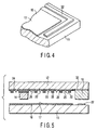
- a groove 19 may be formed in the sealing surface of the front substrate 11, extending along the entire circumference, and the indium layer 32, used as a low melting-point metal material, may be provided in this groove 19.
- the cross section of the groove 18 may be square, round, semicircle form, or arcuate. This embodiment is identical to the first embodiment in terms of other structural aspects and sealing method.
- the indium layer 32 is melted or softened at the time of sealing and accumulated in the groove 19 of the front substrate 11. It remains at a predetermined position, not flowing out of the groove 19. It is therefore easy to handle indium. Therefore, the rear substrate-sidewall assembly and the front substrate can be sealed together both easily and reliably, even if the image display apparatus they constitute is a large one having a large size of 50 inches or more.
- low melting-point glass 30 such as frit glass seals the rear substrates 12 and sidewall 18 which constitute an evacuated envelope 10, as is illustrated in FIG. 9.
- the front substrate 11 and the sidewall 18 are sealed to each other by means of a sealing layer 33 which is composed of a base layer 31 formed on the sealing surface and an indium layer 32 formed on the base layer 31.
- This FED is identical to the first embodiment in any other structural features.
- a front substrate 11 on which a phosphor screen 16 and a metal back 17 are provided, a rear substrate 12 on which electron-emitting elements 22 are provided, and a rectangle frame-like sidewall 18 are prepared by the same method as in the first embodiment. Then, the peripheral edge portion of the rear substrate 12, on which the electron-emitting elements 22 are provided, and the rectangle frame-like sidewall 18 are sealed together, with low melting-point glass 30 in the atmosphere. Simultaneously, a plurality of support members 14 is sealed to the rear substrate 12 in the atmosphere with low melting-point glass 30.
- an base layer 31 having a predetermined width is formed on the upper surface of the sidewall 18 and on the peripheral edge portion of the inner surface of the front substrate 11, which serve as sealing surfaces.
- the base layer 31 is formed by applying silver paste.
- the base layer 31 is coated with indium used as low melting-point metal sealing material.
- An indium layer 32 is thereby formed, extending along the entire of the base layer.
- the indium layer 32 is narrower than the base layer 31. Therefore, the both sides of the indium layer lie at predetermined distances from the sides of the base layer 31, respectively. For example, when the width of a sidewall 18 is 9mm, the base layer 31 and the indium layer 32 are 7mm and about 6mm wide, respectively.
- the low melting-point, metal sealing material is not limited to indium (In). Rather, it may be sliver oxide, silver, gold, copper, aluminum, zinc or tin, or an alloy of at least two of these metals. In97%-Ag3% eutectic alloy, for example, has a lower melting point of 141°C and a greater mechanical strength than indium.
- the base layer 31 is made of material exhibiting good wettability and high air-tightness with respect to the metal sealing material.
- the layer 31 is made of material having affinity with the metal sealing material. It may be made of material other than the metal paste described above. More specifically, it may be made of gold paste, aluminum paste, nickel paste, cobalt paste, or copper paste, or the like. Further, the base layer 31 may be a plated layer or deposited layer of silver, gold, aluminum, nickel, cobalt, copper or the like, or a glass material layer.
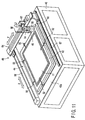
- the sealing-material applying apparatus comprises a supporting base 40 that has a flat mounting surface 40a.
- the hot plate 42 is a flat rectangle board.
- the positioning mechanism 44 is designed to position on the hot plate an object to be sealed.
- the head-moving mechanism 48 is configured to move the applying head 46 relative to the object to be sealed.
- the rear substrate 12 or the front substrate 11 is placed on the hot plate 42.
- the rear substrate 12 is the object to be sealed and that the sidewall 18 is sealed to the hot plate 42.
- the hot plate 42 functions also as means for heating the object to be sealed.
- the positioning mechanism 44 has three positioning claws 50 and two control claws 52.
- the positioning claws 50 are fixed in position. Two of the positioning claws 50 contact one side of the front substrate 11 mounted on the hot plate 42. The remaining positioning claw 50 contacts a side of the front substrate 11, which extends at right angles to said side.
- the control claws 52 contact the other sides of front substrate 11, respectively, to bias the front substrate 11 elastically toward the positioning claws 50.
- the applying head 46 comprises a storage section 54, a nozzle 55, and an ultrasonic vibrator 56.
- the storage section 54 stores molten indium.
- the nozzle 55 receives the molten indium from the storage section 54 and applies the molten indium to the sealing surface of the front substrate 11.
- the ultrasonic vibrator 56 is secured to the outer surface of the nozzle 55 and functions as a section for generating ultrasonic waves.
- a supply pipe 58 for supplying purge gas is connected to the applying head 46.
- the applying head 46 incorporates a heater 60 that heats the nozzle 55.
- the head-moving mechanism 48 comprises a Z-axis drive robot 62 and a Y-axis drive robot 64.
- the Z-axis drive robot 62 supports the applying head 46 to be movable in the Z axis direction that is perpendicular to the mounting surface 40a of the supporting base 40, or to the front substrate 11 placed on the hot plate 42.
- the Y-axis drive robot 64 supports the Z-axis drive robot 62 to be movable back and forth, in the Y axis direction that is parallel to the short sides of the front substrate 11.
- Another X-axis drive robot 66 and an auxiliary rail 67 are secured on the mounting surface 40a. This X-axis drive robot 66 and the auxiliary rail 67 cooperates to support the Y-axis drive robot 64 and move the robot 64 back and forth in the X axis direction that is parallel to the long sides of the front substrate 11.
- the front substrate 11 is placed on the hot plate 12, with the sealing surface turned upward, as illustrated in FIG. 11. Then, the positioning mechanism 44 sets the front substrate 11 at a predetermined position.
- the applying head 46 storing molten indium is set at a applying start position, as shown in FIG. 12.
- the head-moving mechanism 48 moves the applying head 46 a prescribed speed along with the sealing surface of the front substrate 11, i.e., the base layer 31 formed on the front substrate 11. While the applying head 46 is being moved, the nozzle 55 continuously applies the molten indium onto the base layer 32. An indium layer 32 is thereby formed, extending along all sides of the base layer.
- the ultrasonic vibrator 56 is operated, applying ultrasonic waves to the molten indium being so applied from the nozzle 55.
- the ultrasonic waves are applied in a direction perpendicular to the sealing surface of the front substrate 11, i.e., the base layer formed on the front substrate 11.
- the frequency of an ultrasonic wave is set at, for example, 30 to 40 kHz.
- indium is applied while. ultrasonic waves are being applied. Hence, the wettability that the indium has increases, making it possible to fill the indium at any desired position. Further, indium can be continuously applied along the base layer 31, forming an indium layer that extends along all sides of the base layer. Since the molten indium is applied while ultrasonic waves are being applied, a part of the indium can diffuse into the surface of the base layer. An alloy layer can be thereby formed when the process of applying indium is completed.
- the rate of applying indium is controlled by adjusting either the oscillation magnitude of the ultrasonic waves or the diameter of the indium-applying orifice of the indium of a nozzle 55.
- the thickness, width and the like of the indium layer formed can, therefore, be adjusted.
- the rear substrate 12 is positioned on the hot panel 42 of the sealing-material applying apparatus, as has been described above.
- the applying head 46 continuously applies molten indium along the base layer 31, while applying ultrasonic waves. An indium layer 32 is thereby formed, continuously extending along the base layer 31.
- the front substrate 11 and the rear substrate-sidewall assembly are held with a jig or the like, with their sealing surfaces opposing each other and spaced from each other by a predetermined distance.
- the base layer 31 and the indium layer 32 are provided on the sealing surface of the front substrate 11.
- the rear substrate-sidewall assembly comprises the rear substrate 12, the sidewall 18 sealed thereto, and the base layer 31 and the indium layer 32, both formed on the upper surface of the sidewall 18.
- the front substrate 11 and the rear substrate-sidewall assembly are inserted into the vacuum process apparatus 100 described earlier.
- the front substrate 11 and the rear substrate-sidewall assembly are heated, as in the first embodiment, to a temperature of about 300°C and thereby baked when the degree of vacuum reaches a high value of about 10 -5 Pa.
- the surface adsorption gas is fully released from each component.
- the indium layer 32 (having a melting point of about 156°C) melts. However, the indium remains on the base layer 31, not flowing from the layer 31, because the indium layer 32 is formed on the base layer 31 that exhibits high affinity with indium. This prevents indium from flowing to the electron-emitting-elements 22, flowing from the rear substrate or to the phosphor screen 16.
- the rear substrate-sidewall assembly and the front substrate 11 are cooled to a temperature of about 100°C in the cooling chamber 103, after they have been heated and washed with an electron beam. Then, in the vacuum evaporation chamber 104, vacuum evaporation formation of a Ba film is formed as getter film, outside the phosphor screen, by means of vapor deposition.
- the rear substrate-sidewall assembly and the front substrate 11 are transferred into the assembling chamber 105.
- the assembly and the front substrate 11 are heated to 200°C.
- the indium layer 32 melts or softens to assume liquid state again.
- the front substrate 11 and the sidewall 18 are joined together.
- a predetermined pressure is applied to the front substrate 11 and the sidewall 18.
- the indium is gradually cooled and solidified.
- the sealing layer 33 which fuses the indium layer 32 and the base layer 31 together, connects the front substrate 11 and the sidewall 18.
- An evacuated envelope 10 is thereby formed.
- the evacuated envelope 10 thus formed is cooled to normal temperature in the cooling chamber 106.
- the evacuated envelope 10 is removed from the unloading chamber 107.
- An FED is thereby manufactured by performing the above-mentioned sequence of process.
- the front substrate 11 and the rear substrate 12 are sealed together in a vacuum atmosphere.
- the surface adsorption gas is therefore fully released as the substrate 11 and the assembly are baked and washed with an electron beam.
- the getter film remains not oxidized, and a sufficient gas adsorption effect can be accomplished.
- the FED obtained can therefore maintain a high degree of vacuum.
- indium is used as sealing material, foaming can be suppressed at the time of the sealing process. This makes it possible to provide an FED having high air-tightness and great sealing strength.
- indium can be prevented from flowing though it melts in the sealing process. This is because the base layer 31 is formed in the bottom of the indium layer 32. The indium layer remains at the predetermined position. That is, it is easy to handle indium. Thus, the components can be easily and reliably sealed to one another, even if they form a large-sized, 50-inch image display apparatus.
- the wettability of indium to any sealing surface or the base layer 31 improves because indium is applied while ultrasonic waves are applied.
- Indium used as metal sealing material can be applied at a desired position. Molten indium can be continuously applied along the base layer 31. An indium layer can thereby be formed, extending, without breaks, along with the base layer.
- molten indium is applied while ultrasonic waves are being applied. In this case, a part of the indium applied diffuses into the surface of the base layer 31, forming an alloy layer. Even if the indium melts at the time of sealing, it is prevented from flowing. The molten indium reliably remains at the predetermined position.
- the invention can provide a method of manufacturing an image display apparatus, which can perform sealing easily and reliably in a vacuum.
- the base layer 31 and the indium layer 32 are formed on both the sealing surface of the front substrate 11 and the sealing surface of the sidewall 18, and the base layer 31 and the sidewall 18 are sealed together. Nonetheless, a base layer 31 and an indium layer 32 may be formed on only the sealing surface of either the front substrate 11 or the sidewall 18. For example, a base layer 31 and an indium layer 32 may be formed on the sealing surface of the front substrate 11 as illustrated in FIG. 14.
- an indium layer may be formed directly on the sealing surface of the substrate or sidewall, without using a base layer.
- molten indium may be applied, while applying ultrasonic waves in the sealing-material applying apparatus described above.
- the wettability that the indium layer exhibits with respect the sealing surface therefore improves.
- indium can be continuously applied at a desired position.
- a sealing layer 33 that seals the base layer 31 and the indium layer 32 may be used to fuse the rear substrate 12 and the sidewall 18 together. Further, the peripheral edge portion of the front substrate or the peripheral edge portion of the rear substrate may be bent, and these substrates may be coupled together at the edge portion, using no sidewalls.
- the indium layer 32 need not have, in its entirety, a width smaller than that of the base layer 31. Rather, it suffices for the layer 32 to have at least one part that is less wide than the base layer 31. In this case, too, it is possible to prevent indium from flowing.
- low melting-point glass 30 such as a frit glass, seals the rear substrate 12 and the sidewall 18 that form an evacuated envelope 10, as is illustrated in FIG. 15.
- the FED is identical in structure to the first embodiment in any other structural aspects.
- the front substrate 11, the rear substrate 12, and the sidewall 18 are prepared in the same way as in the first embodiment.
- the front substrate 11 comprises a phosphor screen 16 and a metal back 17.
- the rear substrate 12 has electron-emitting elements 22 provided on it.
- the edges of the rear substrate 12, on which the electron-emitting elements 22 are formed are sealed to the sidewall 18 shaped like a rectangle frame, with low melting-point glass 30 in the atmosphere.
- a plurality of support members 14 is sealed to the rear substrate 12 with low melting-point glass 30 in the atmosphere.
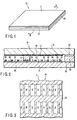
- a base layer 31 is formed on the inner surfaces of all edge parts of the front substrate 11, which serve as a sealing surface 11a of the front substrate 11, as shown in FIGS. 16A, 16B and 17.
- the sealing surface 11a is shaped like a rectangular frame and corresponds to the upper surface of the sidewall 18 that serves as the sealing surface 18a of the rear substrate 12.
- the sealing surface 11a extends along the peripheral edge of the front-substrate 11.
- the surface 11a has two sets of straight parts and four corner parts. The straight parts of each set oppose each other.
- the sealing surface 11a has almost the same dimension and the same width as the upper surface of the sidewall 18.
- the base layer 31 is formed, a slightly less wide than sealing surface 11a.
- the base layer 31 is formed by applying silver paste.
- indium is applied as metal sealing material onto the base layer 31, thus forming an indium layer 32.
- the indium layer 32 continuously extends, without breaks, along the base layer 31.
- Those portions of the indium layers 32, which extend along the straight parts of sealing surface 11a, comprise each a rigid-frame like patterns. These patterns are arranged at a predetermined pitch and have sharply bent parts 32a each.
- the indium layer 32 has an almost fixed width. Both sides of the indium layer 32 have many bent parts, too. Note that the indium layer 32 lies on base layer 31, not extending from the layer 31.
- the metal sealing material used is identical to those used in the other embodiments described above.
- the base layer is made of the same identical as those of the other embodiments.
- the front substrate 11 having the base layer 31 and the indium layer 32 formed on the sealing surface 11a, and the rear substrate-sidewall assembly comprising the rear substrate 12 and the sidewall 18 sealed to the substrate 12 are held by a jig or the like, with the sealing surfaces 11a and 18a opposing each other and spaced apart by a predetermined distance, as shown in FIG. 18.
- the front substrate 11 and the rear substrate-sidewall assembly, thus held, are inserted into the vacuum process apparatus 100 described above.
- the assembly and the front substrate 11 are transferred into the baking/electron-beam washing chamber 102.
- a baking/electron-beam washing chamber 102 the rear substrate-sidewall assembly and the front substrate are heated to a temperature of about 300°C and are thereby backed, when the vacuum attains a degree of about 10 -5 Pa.
- the surface-adsorbed gas is fully released from every component of the assembly and the front substrate.
- the indium layer 32 (having melting point of about 156°C) melts. Nonetheless, molten indium is prevented from flowing, because the indium layer 32 is provided in the form of the pattern having a number of bent parts 32a, as indicated above.
- the indium layer 32 is formed on the base layer 31 that exhibits high affinity with indium, the molten indium remains on the base layer 31, not flowing from the layer 31. Thus, the molten indium would not flow from the base layer 31 to the electron-emitting-elements 22, from the rear substrate, or to the phosphor screen 16.
- the rear substrate-sidewall assembly and the front substrate 11 are cooled to a temperature of about 100°C in the cooling chamber 103, after they have been heated and washed with an electron beam. Then, in the vacuum evaporation chamber 104, vacuum evaporation formation of a Ba film is formed as getter film, outside the phosphor screen, by means of vapor deposition.
- the rear substrate-sidewall assembly. and the front substrate 11 are transferred into the assembling chamber 105.
- the assembly and the front substrate 11 are heated to 200°C.
- the indium layer 32 melts or softens to assume liquid state again. Since the indium layer 32 is formed in the shape of the pattern having a number of bent part 32a and is formed on the base layer 31 exhibiting high affinity with indium, as indicated above, the molten indium remains on the base layer 31, not flowing from the layer 31.
- the front substrate 11 and the sidewall 18 are joined together in this condition.
- a predetermined pressure is applied to the front substrate 11 and the sidewall 18.
- the indium is gradually cooled and solidified.
- the sealing layer 33 which fuses the indium layer 32 and the base layer 31 together, connects the front substrate 11 and the sidewall 18. An evacuated envelope 10 is thereby formed.
- the evacuated envelope 10 thus formed is cooled to normal temperature in the cooling chamber 106.
- the evacuated envelope 10 is removed from the unloading chamber 107.
- An FED is thereby manufactured by performing the above-mentioned sequence of process.
- the front substrate 11 and the rear substrate 12 are sealed together in a vacuum atmosphere.
- the surface adsorption gas is therefore completely released as the substrate 11 and the assembly are baked and washed with an electron beam.
- the getter film remains not oxidized, and a sufficient gas adsorption effect can be accomplished.
- the FED obtained can therefore maintain a high degree of vacuum.
- indium is used as sealing material, foaming can be suppressed at the time of the sealing process. This makes it possible to provide an FED having high air-tightness and great sealing strength. Further, the indium, if melted during the sealing process, can remain at a prescribed position, not flowing from the position, because the indium layer 32 is formed in a pattern having a number of bent parts 32a. Hence, it is easy to handle indium. The components can be easily and reliably sealed to one another, even if they form a large-sized, 50-inch image display apparatus.
- the indium layer 32 is formed on the high base layer 31 that exhibits high affinity with indium. Therefore, indium, if melting during the sealing process, is more reliably prevented from flowing than in the other embodiments. This renders it possible to accomplish easy and reliable sealing.
- the indium layer 32 extends along all straight edges of the sealing part 11a and each portion extending one edge of the sealing part 11a has a number of bent parts over its entire length. Nevertheless, each portion of the layer 32 may have bent parts or curbed parts at only one part or more. In this case, too, the molten indium can be prevented from flowing as in the embodiment described above.
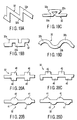
- the patterns constituting the indium layer 32 is not limited to frame-structure ones. Rather, they may be such patterns as illustrated in FIG. 19A to FIG. 19D.
- the patterns of FIG. 19A to FIG. 19D result in the same functional advantage.
- the indium layer 32 may have the saw-toothed pattern of FIG. 19A, consisting of bent parts 32, each bent at an acute angle ⁇ . It may have a crank-shaped pattern of FIG. 19B, having bent parts 32 bent at almost right angles. It may have the pattern of FIG. 19C consisting of bent parts, each bent in the form of an inverted triangle. It may have the waving pattern of FIG. 19D, consisting of arcuate parts 32b.
- the indium layer 32 may have a pattern that consists of bent parts and curved parts.
- the indium layer 32 has fixed width. Nonetheless, the indium layer may consist of parts having different widths so that one side or both sides are undulated.
- rectangular projections 40 may protrude from both sides of the layer 32 and spaced apart in the lengthwise direction of the layer 32, as is illustrated in FIG. 20A or FIG. 20C.
- semicircular projections 41 may protrude from both sides of the layer 32 and spaced apart in the lengthwise direction of the layer 32, as is shown in FIGS. 20B and 20D.
- the projections 40 and 41 may be arranged as shown in FIGS. 20A and 20B, each overlapping the nearest one projecting from the opposite side of the layer 32.
- the projections 40 and 41 may be arranged as shown in FIGS. 20C and 20D, each staggered with respect to nearest one projecting from the opposite side of the layer 32.
- the shape of projections is not limited to a rectangular one and an arcuate one. Any other shape can be selected for the projections. Moreover, the projections only need to protrude from at least one side of the indium layer 32, to prevent the molten indium from flowing.
- a base layer is formed on a sealing surface and an indium layer is formed on the base layer.
- no base layer may be formed and an indium layer may be formed directly on the sealing surface.
- indium may be applied while ultrasonic waves are being applied, as in the second embodiment.
- the sealing process is carried out, with the base layer 31 the indium layer 32 formed on only the sealing surface 11a of the front substrate 11. Nonetheless, the process may be performed, with the layers 31 and 32 formed on only the sealing surface 18a of the sidewall 18, or, as shown in FIG. 21, on both the sealing surface 11a of the front substrate 11 and the sealing surface 18a of the sidewall 18.
- the present invention is not limited to the embodiment described above. Various modifications can be made within the scope of the invention.
- the rear substrate and the a sidewall may be sealed together, by using a sealing layer that comprises a base layer and an indium layer, which are similar to the layers 31 and 32 described above.
- the front substrate or the rear substrate may be bent at one edge and directly coupled to each other, with no sidewall interposed between them.
- the electron-emitting elements used are of field emission type.
- the electron-emitting elements are not limited to this type.
- the electron-emitting elements may be of other type, for example, pn type cold-cathode elements, surface conduction type electron-emitting elements, or microchip type electron-emitting elements.
- this invention can be applied to image display apparatuses of other types, such as plasma display panels (PDP) and electroluminescence (EL) apparatuses.
- PDP plasma display panels
- EL electroluminescence
- the substrates forming an envelope can be easily sealed together in a vacuum atmosphere, by using a metal sealing material. They are sealed at a low temperature that does no thermal damages to electron-emitting elements and the like. Further, no bubbles are generated in the sealing material and the like. This helps to improve the air-tightness of the envelope and the sealing strength. Therefore, the invention can provide an image display apparatus that can display high-quality images and can also provide a method of manufacturing such an image display apparatus.
Landscapes
- Engineering & Computer Science (AREA)
- Manufacturing & Machinery (AREA)
- Manufacture Of Electron Tubes, Discharge Lamp Vessels, Lead-In Wires, And The Like (AREA)
- Cathode-Ray Tubes And Fluorescent Screens For Display (AREA)
- Vessels, Lead-In Wires, Accessory Apparatuses For Cathode-Ray Tubes (AREA)
Abstract
The evacuated envelope (10) of an image display
apparatus has a rear substrate (12), a front substrate
(11) opposing the rear substrate (12), and a sidewall
(18) interposed between the rear and front substrates.
A phosphor screen (16) is formed on the inner surface
of the front substrate 11. Electron-emitting elements
(22) are provided on the rear substrate. An indium
layer (32) is formed on a sealing surface lying between
the front substrate and the sidewall. When the indium
layer is heated and melted in a vacuum atmosphere, the
front and rear substrates are sealed to each other,
with the sidewall interposed between them.
Description
The present invention relates to a flat, planar-type
image display apparatus comprising an evacuated
envelope, a method of manufacturing the image display
apparatus, and a sealing-material applying apparatus.
In recent years, display apparatuses have been
developed as next- generation, lightweight, thin,
planar-type displays. These apparatus comprise a
phosphor screen and a number of electron-emitting
elements (hereinafter called "emitters"). The emitters
are arranged, opposing the phosphor screen. The
emitters may be of either field emission type or
surface conduction type. Display apparatuses using
field emission type electron-emitting elements as
emitters are generally called "field emission displays"
(hereinafter referred to as "FEDs"). Display
apparatuses using surface conduction type electron-emitting
elements as emitters are generally called
"surface conduction type electronic discharge display"
(hereinafter referred to as "SEDs").
For example, FEDs generally have a front substrate
and a rear substrate opposing each other and spaced
apart by a predetermined distance. These substrates
constitute an evacuated envelope, because they are
coupled together at their circumferential edges, with
a rectangle frame-like sidewall interposed between
them. The phosphor screen is formed on the inner
surface of the front substrate. A number of emitters
are provided on the inner surface of the rear
substrate. The emitters are used as electron-emitting
sources. The electrons they emit excite phosphor
layers, causing the phosphor layers to emit light.
A plurality of support members are interposed between
the front substrate and the rear substrate to withstand
atmospheric pressure applied on these substrates.
The electric potential at the rear substrate is
about 0V. The anode voltage Va is applied to the
phosphor screen. The electron beams emitted from the
emitters are applied to the red phosphor layers, that
constitute the phosphor screen, to energize the
phosphor layers, whereby an image is displayed.
In such a FED, the distance between the front
substrate and the rear substrate can be set at several
millimeters or less. Therefore, FED is lighter and
thinner than the cathode-ray tube (CRT) used at present
as a display of televisions or computers.
It is necessary to maintain the degree of vacuum
inside the evacuated envelope at 10-5 to 10-6 Pa in
the planar display apparatus described above. In the
conventional evacuation method, the surface adsorption
gas inside the envelope is liberated by performing
baking in which the envelope is heated to about 300°C.
The evacuation method cannot completely liberate the
surface adsorption gas.
Jpn. Pat. Appln. KOKAI Publication No. 9-82245,
for example, discloses a planar display apparatuses of
various structures. In one structure disclosed, getter
material such as Ti, Zr or alloy thereof covers the
metal back that is formed on the phosphor screen of the
front substrate. In another structure disclosed, the
metal back is made of getter material. In still
another structure disclosed, getter material covers the
components other than the electron-emitting elements,
in the image-displaying region.
In the image display apparatus disclosed in Jpn.
Pat. Appln. KOKAI Publication No. 9-82245, getter
material is formed in the ordinary panel process.
Inevitably, the surface of getter material will be
oxidized. The getter material is highly active at the
surface. Once oxidized at surface, the getter material
can no longer adsorb gas as much as desired.
A method of enhancing the degree of vacuum inside
the evacuated envelope may be considered. In this
method, a rear substrate, a sidewall, and a front
substrate are brought into a vacuum chamber. These
components are baked in the vacuum atmosphere and
irradiated with an electron beam. The surface
adsorption gas is thereby released from the rear
substrate, sidewall and front substrate. Thereafter, a
getter film is formed, and the sidewall, rear substrate
and front substrate are sealed together, with frit
glass or the like, in the vacuum atmosphere. This
method can release the surface adsorption gas
sufficiently by means of electron-beam washing. The
getter film is not oxidized. A sufficient gas
adsorption can be accomplished. In addition, the space
in the image display apparatus is not wasted because no
evacuation pipes are necessary.
However, to fuse the components together in a
vacuum atmosphere by using frit glass, the frit glass
must be heated to a high temperature of 400°C or more.
When so heated, the frit glass generates air bubbles.
This degrades the air-tightness, sealing strength and
the like of the evacuated envelope. Consequently, the
reliability of the image display apparatus decreases.
In view of the characteristic of the electron-emitting
elements, it may be desirable not to heat the frit
glass to 400°C or more. In such a case, the method of
sealing the components with frit glass is not
desirable.
This invention has been made in view of the
foregoing. An object of the invention is to provide
an image display apparatus comprising an envelope which
can be easily sealed and which can maintain a high
vacuum, to provide a method of manufacturing the image
display apparatus, and to provide a sealing-material
applying apparatus.
To attain the object, an image display apparatus
according to this invention comprises an envelope
having a rear substrate, a front substrate opposing
the rear substrate, and a number of electron-emitting
elements provided in the envelope.
The front substrate and the rear substrate are
sealed, at edge parts, either directly or indirectly to
each other with low melting-point metal sealing
material.
In the image display apparatus according to the
invention, it is preferred that the low melting-point
metal sealing material preferably have a melting point
of 350°C or less. Further, it is desired that the low
melting-point metal sealing material be indium or
an alloy containing indium.
According to the invention, there is provided
a method of manufacturing an image display apparatus
which comprises an envelope having a rear substrate,
a front substrate opposing the rear substrate, and
a number of electron-emitting elements provided in the
envelope. The method comprises the steps of: applying
low melting-point metal sealing material to a sealing
surface lying between the rear substrate and the front
substrate; and sealing the rear substrate and the front
substrate together, either directly or indirectly to
each other, by heating the rear substrate and the front
substrate in a vacuum atmosphere and by melting the low
melting-point metal sealing material.
In the method of manufacturing an image display
apparatus, it is preferred that the low melting-point
metal sealing material have a melting point of 350°C or
less. Moreover, it is desired that the low melting-point
metal sealing material be indium or an alloy
containing indium. The degree of vacuum in the
envelope is preferably 10 -3 Pa or less.
In the method of manufacturing an image display
apparatus, according to the invention, the sealing the
rear substrate and the front substrate together
includes an evacuating step of heating the vacuum
atmosphere to a temperature of 250°C or more; a sealing
step of sealing the front substrate and the rear
substrate by applying the low melting-point metal
sealing material to a sealing surface lying between
the front and rear substrates, at a temperature lower
than the temperature used in the evacuating step; and
a step of bringing the envelope sealed with the low
melting-point metal sealing material, back into the
atmosphere. The sealing may be performed by using
the low melting-point metal sealing material at
a temperature of 60 to 300°C.
In a method of manufacturing an image display
apparatus, according to this invention, in the sealing
step, the front and rear substrates are moved relative
to each other and are sealed to each other after low
melting-point metal sealing material is applied to
sealing surfaces lying between the front substrate and
the rear substrate. The direction in which the rear
plate and the front substrate are moved relative to
each other may be any direction in a three-dimensional
space, so long as the substrates approach each other.
Only one of the substrates may be moved, or both
substrates may be moved.
In the method of manufacturing an image display
apparatus, according to this invention, a material-retaining
section is provided to retain the low
melting-point metal sealing material, at least of the
sealing surfaces lying between the front substrate and
the rear substrate. The low melting-point metal
sealing material is applied onto the material-retaining
section.
The material-retaining section is preferably a
groove formed in the sealing surface or a layer formed
on the sealing surface and made of material that
exhibits high affinity with the low melting-point metal
sealing material. The material exhibiting high
affinity with the low melting-point metal sealing
material is preferably nickel, gold, silver or copper,
or an alloy thereof.
In the image display apparatus and the method of
manufacturing the same, both according to the present
invention, the. front and rear substrates forming an
envelope can be sealed together in a vacuum atmosphere,
by using low melting-point metal sealing material.
They are sealed at a low temperature (about 300°C or
less) that does no thermal damages to the electron-emitting
elements and the like. Any components
required in the conventional method, such as thin
evacuation pipes, are unnecessary, and the evacuation
efficiency can be very high.
Hence, the invention can provide image display
apparatuses that have an envelope maintaining a high
degree of vacuum and are free of an image-quality
decrease due to thermal deterioration of the electron-emitting
elements.
An image display apparatus according to another
aspect of the present invention comprises an envelope
having a rear substrate, a front substrate opposing the
rear substrate, and a plurality of electron-emitting
elements provided in the envelope. The front substrate
and the rear substrate are sealed either directly or
indirectly to each other with a base layer and a metal
sealing material layer provided on the base layer and
different in material from the base layer.
An image display apparatus according to this
invention comprises an envelope having a rear
substrate, a front substrate opposing the rear
substrate and a sidewall arranged between edges of the
front substrate and edges of the rear substrate, and a
plurality of electron-emitting elements provided on an
inner surface of the rear substrate and configured to
emit electron beams. The front substrate and the
sidewall, or the rear substrate and the sidewall, or
the front substrate and the side wall and the rear
substrate and the side wall are sealed together with a
base layer and a metal sealing material layer different
in material from a material of the base layer.
In this image display apparatus, the metal sealing
material layer is made of low melting-point metal
sealing material having a melting point of 350°C or
less. For example, the low melting-point metal sealing
material may be indium or an alloy containing indium.
Preferably, the base layer is made of metal paste
containing at least one element selected from the group
consisting of silver, gold, aluminum, nickel, cobalt
and copper. Alternatively, the base layer may be a
plated layer or deposited layer made of at least one
element selected from the group consisting of silver,
gold, aluminum, nickel, cobalt and copper. Still
alternatively, it may be made of glass material or the
like.
In the image display apparatus and the method of
manufacturing the same, both described above, the front
substrate and the rear substrate are sealed with metal
sealing material, either directly or indirectly to each
other. Therefore, the substrates can be sealed
together at a low temperature that does no thermal
damages to the electron-emitting elements or the like.
A number of bubbles will not develop as in the case
where frit glass or the like is used. This helps to
improve the air-tightness and sealing strength of the
envelope. Moreover, the base layer, which is different
in material from the metal sealing material layer,
prevents the metal sealing material from flowing, thus
retaining the material at a predetermined position,
even when the metal sealing material melted to have its
viscosity reduced. Hence, the invention can provide an
image display apparatus and a method of manufacturing
the same, in which the metal sealing material can
easily be treated and the sealing step can be performed
in a vacuum atmosphere easily and reliably.
According to this invention, there is provided
a method of manufacturing an image display apparatus
which comprises an envelope having a rear substrate,
a front substrate opposing the rear substrate, and
a plurality of electron-emitting elements provided in
the envelope. This method comprises applying molten
metal sealing material to a sealing surface lying
between the rear substrate and the front substrate,
while applying ultrasonic waves; and heating and
melting the metal sealing material in a vacuum
atmosphere after the metal sealing material has been-applied,
and sealing the rear substrate and the front
substrate at the sealing surface, either directly or
indirectly to each other.
According to the invention, there is provided
a method of manufacturing an image display apparatus
which comprises an envelope having a rear substrate,
a front substrate opposing the rear substrate,
a sidewall arranged between edges of the front
substrate and edges of the rear substrate; and
a plurality of electron-emitting elements provided in
the envelope, wherein the front substrate and the
sidewall, or the rear substrate and the sidewall, or
the front substrate and the side wall and the rear
substrate and sidewall are sealed together with a metal
sealing material layer. The method comprises the steps
of: applying molten metal sealing material to a sealing
surface lying between the rear substrate and the front
substrate, while applying ultrasonic waves; and heating
and melting the metal sealing material in a vacuum
atmosphere after the metal sealing material has been
applied, and sealing the rear substrate, the front
substrate and the sidewall together at the sealing
surface.
In this method of manufacturing an image display
apparatus, according to the invention, the step of
applying the metal sealing material includes a step of
continuously applying the molten metal sealing material
along the sealing surface, thereby forming a metal
sealing material layer that extends along the sealing
surface.
The method of manufacturing an image display.
apparatus, according to this invention may comprise
a step of forming a base layer on the sealing surface.
The base layer is different in material from the metal
sealing material layer. In this method, the metal
sealing material is applied onto the base layer after
the base layer has been formed.
In the method of manufacturing an image display
apparatus, according to the invention, the metal
sealing material may be low melting-point metal sealing
material that has a melting point of 350°C or less.
The material is, for example, indium or an alloy
containing indium. Preferably, the base layer is
made of material that exhibits good wettability and
air-tightness with respect to the metal sealing
material. In other words, it should be made of
material exhibiting high affinity with the metal
sealing material. The base layer may be made by
applying metal paste containing at least one element
selected from the group consisting of silver, gold,
aluminum, nickel, cobalt, copper nickel, gold, silver
and copper. Alternatively, it may be a plated layer or
deposited layer made of at least one element selected
from the group consisting of silver, gold, aluminum,
nickel, cobalt and copper, or is a glass material
layer.
In the method of manufacturing an image display
apparatus, described above, the front substrate and the
rear substrate are sealed by using a metal sealing
material layer, either directly or indirectly to each
other. The substrates can therefore be sealed together
at such a low temperature as would not do thermal
damages to the electron-emitting elements and the like
provided on the rear substrate. Further, a number of
bubbles will not develop as in the case where frit
glass or the like is used. This helps to improve the
air-tightness and sealing strength of the envelope.
In addition, the metal sealing material has its
wettability to the sealing surface improved, because
ultrasonic waves are applied while the metal sealing
material is being applied to the sealing surface.
Thus, the metal sealing material can remain at
a desired position even if it is indium or the like.
Hence, the present invention can provide a method of
manufacturing an image display apparatus, in which
the components can be sealed together in a vacuum
atmosphere, both easily and reliably.
The molten metal sealing material may be
continuously applied along the sealing surface, while
ultrasonic waves are being applied. Thus applied, the
material can form a metal sealing material layer that
extends along the sealing surface, without breaks.
A base layer, different in material from the metal
sealing material, is formed on the sealing surface.
Then, the metal sealing material is applied onto the
base layer while ultrasonic waves are being applied.
Hence, even if the metal sealing material applied is
heated and melted, the base layer prevents the molten
metal sealing material from flowing. That is, the base
layer holds the molten material at a predetermined
position. It is therefore easy to treat the metal
sealing material. The sealing step can be performed in
a vacuum atmosphere, both easily and reliably. In
particular, a part of the metal sealing material
diffuses into the base layer, forming an alloy layer,
when the material is applied while ultrasonic waves are
being applied. This more reliably prevents the metal
sealing material from flowing and holds the same at the
predetermined position, in the course of the sealing
step.
In the step of applying the metal sealing
material, the rate at which the metal sealing material
is applied can be controlled by changing either output
magnitude of the ultrasonic waves or a diameter of
a port for applying the metal sealing material.
An apparatus for applying metal sealing material,
according to the present invention, comprises: a
supporting base for positioning an object having a
sealing surface; an applying head having a storage
section storing molten metal sealing material, a nozzle
which applies to the sealing surface the molten metal
sealing material supplied from the storage section, and
an ultrasonic wave generating section which applies
ultrasonic waves to the molten metal sealing material
applied from the nozzle to the sealing surface; and
a head-moving mechanism which moves the applying head
relative to the sealing surface.
An image display apparatus according to this
invention comprises an envelope having a rear
substrate, a front substrate opposing the rear
substrate and sealed either directly or indirectly to
the rear substrate with metal sealing material, and a
number of electron-emitting elements provided in the
envelope. The metal sealing material is provided on a
sealing surface lying between the rear substrate and
the front substrate, forming a metal sealing material
layer that extends along the entire of the sealing
surface. The metal sealing material layer has bent or
curved parts at one portion, at least, which extends
along a straight part of the sealing surface.
An image display apparatus according to the
present invention comprises an envelope having a rear
substrate, a front substrate opposing the rear
substrate and sealed either directly or indirectly to
the rear substrate with metal sealing material, and a
number of electron-emitting elements provided in the
envelope. The metal sealing material is provided on a
sealing surface lying between the rear substrate and
the front substrate, forming a metal sealing material
layer that extends along the entire of the sealing
surface. The metal sealing material layer has an edge
at one portion, at least, which extends along a
straight part of the sealing surface. The edge has
projections.
A method according to the invention is designed to
manufacture an image display apparatus comprising an
envelope having a rear substrate, a front substrate
opposing the rear substrate and sealed either directly
or indirectly to the rear substrate with metal sealing
material, and a number of electron-emitting elements
provided in the envelope. The method comprises the
steps of: applying metal sealing material to a sealing
surface laying between the rear substrate and the front
substrate, thereby forming a metal sealing material
layer which extends along the entire of the sealing
surface; and heating and melting the metal sealing
material in a vacuum atmosphere after the metal sealing
material has been applied, and sealing the rear
substrate and the front substrate at the sealing
surface, either directly or indirectly to each other.
In the step of applying the metal sealing material,
bent or curved parts are formed at one portion, at
least, of the metal sealing material layer. The
portion extends along a straight part of the sealing
surface.
In another method of manufacturing an image
display apparatus, according to the invention,
comprises the steps of: applying metal sealing material
on a sealing surface lying between the rear substrate
and the front substrate, thus forming a metal sealing
material layer that extends the entire of the sealing
surface; and heating and melting the metal sealing
material in a vacuum atmosphere after the metal sealing
material has been applied, thus sealing the rear
substrate and the front substrate at the sealing
surface, either directly or indirectly to each other.
In the step of applying the metal sealing material, the
material is applied such that projections are formed at
one portion, at least, of the metal sealing material
layer. The portion extends along a straight part of
the sealing surface.
In both the image display apparatus and the method
of manufacturing the same, both according to this
invention, the metal sealing material may be low
melting-point metal sealing material that has a melting
point of 350°C or less. The material is, for example,
indium or an alloy containing indium.
In both the image display apparatus and the method
of manufacturing the same, described above, the front
substrate and the rear substrate are sealed by using a
metal sealing material layer, either directly or
indirectly to each other. The substrates can therefore
be sealed together at such a low temperature as would
not do thermal damages to the electron-emitting
elements and the like provided on the rear substrate.
Further, a number of bubbles will not develop as in the
case where frit glass or the like is used. This serves
to enhance the air-tightness and sealing strength of
the envelope.
Moreover, one portion, at least, of the metal
sealing material layer, which extends along a straight
part of the sealing surface, has bent or curved parts.
Alternatively, one portion, at least, of the metal
sealing material layer, which extends along a straight
part of the sealing surface, has projections. The bent
parts, the curved parts, or the projections prevent the
metal sealing material from flowing, thus retaining the
material at a predetermined position, even when the
metal sealing material melted to have its viscosity
reduced. That is, they can hold the material at a
predetermined position. The invention can therefore
provide an image display apparatus and a method of
manufacturing the same, in which the metal sealing
material can easily be treated and the sealing step can
be performed in a vacuum atmosphere, both easily and
reliably.
Hereafter, an embodiment of the invention, which
is an image display apparatus of this invention, i.e.,
an FED, will be described in detail with reference to
the accompanying drawings.
As FIG. 1 and 2 show, the FED comprises a front
substrate 11 and a rear substrate 12. The substrates
11 and 12 are rectangular glass plates and serve as
insulating substrates. The substrates oppose each
other, spaced apart by a distance of about 1.5 to
3.0 mm. The front substrate 11 and the rear substrate
12 are sealed together at their circumferential edges,
with a rectangular frame-shaped sidewall 18 interposed
between them, thereby constituting an evacuated
envelope 10. The envelope 10 is flat and rectangular,
maintaining a vacuum in it.
A plurality of support members 14 are provided in
the evacuated envelope 10. The members 14 withstand
atmospheric pressure exerted on the rear substrate 12
and the front substrate 11. The support members 14
extend parallel to the long sides of the evacuated
envelope 10 and are spaced apart by a prescribed
distance in the direction parallel to the short sides
of the envelope 10. The shape of the support
members 14 is not limited to this. The members 14 may
be shaped like pillars.
As FIG. 3 shows, a phosphor screen 16 is formed on
the inner surface of the front substrate 11.
The phosphor screen 16 comprises phosphor layers R, G
and B which can emit red light, green light and blue
light, respectively, and the matrix-shaped, light-absorbing
black part 20. The support members 14 are
placed behind the light-absorbing black part 20.
A metal back layer 17 is provided on the phosphor
screen 16. The layer 17 is a conductive thin film,
such as aluminum film. The metal back layer 17
reflects that part of the light generated by the
phosphor screen 16, which travels toward the rear
substrate 2 that serves as an electron source. The
layer 17 therefore increases luminosity. The metal
back layer 17 imparts conductivity to the image-displaying
region of the front substrate 11, thus
preventing accumulation of electric charges. Hence,
the layer 17 functions as an anode for the electron-emitting
source provided on the rear substrate 12,
which will be described later. The layer 17 performs
another function; it protects the phosphor screen 16
from damages due to the ions generated when gas in the
evacuated envelope 10 is ionized with an electron beam.
As shown in FIG. 2, a number of electron-emitting
elements 22 of field emission type are provided on the
inner surface of the rear substrate 12. The electron-emitting
elements 22 are sources of electrons and emit
an electron beam that excites the phosphor layers R, G
and B. The electron-emitting elements 22 correspond to
pixels, respectively. They are arranged in rows and
columns and function as pixel-displaying elements in
this invention.
More specifically, a conductive cathode layer 24
is formed on the inner surface of a rear substrate 12.
A silicon dioxide film 26 having many cavities 25 is
formed on the cathode layer. On the silicon dioxide
film 26, cone-shaped gate electrodes made of molybdenum
or the like are formed in the cavities 25 made in the
inner surface of the rear substrate 12. Wires (not
shown) and the like, which are arranged in the form of
a matrix, are formed on the rear substrate 12 and are
connected to the electron-emitting elements 22.
In the FED described above, video signals are
input into the electron-emitting elements 22 and the
gate electrodes 28 which were arranged in the form of a
simple matrix. If the electron-emitting elements 22
are used as reference, a gate voltage of +100V is
applied in a state of the highest luminosity. A
voltage of +10kV is applied to the phosphor screen 16.
The intensity of the electron beam emitted from each
electron-emitting element 22 is modulated by the
voltage applied to the gate electrode 28. An image is
displayed when the electron beam excites the phosphor
layers of the phosphor screen 16, causing the phosphor
layers to emit light.
The high voltage is thus applied to the phosphor
screen 16. Therefore, a high strain point glass is
used for the glass plates constituting the front
substrate 11, rear substrate 12, sidewall 18 and
support-member 14. Low melting-point glass 30, such as
a frit glass, seals the rear substrate 12 and the
sidewall 18 together, as will be described later. The
front substrate 11 and the sidewall 18 are sealed
together by means of a layer 32 of low melting-point
metal such as indium (In) which is formed on the
sealing surface.
Next, a method of manufacturing the FED
constituted as described above will be described in
detail.
First, a phosphor screen 16 is formed on the glass
plate used as a front substrate 11. The screen 16 is
made by the following method. First, a glass plate of
the same size as the front substrate 11 is prepared. A
pattern of phosphor layers is formed on the glass plate
by means of a plotter machine. The glass plate, with
the phosphor pattern formed on it, is mounted on a
positioning jig. The jig holding the phosphor pattern
is placed on an exposure table. Then, the pattern is
exposed to light and developed, providing the phosphor
screen 16.
Next, an Al film having a thickness of 2500 nm or
less is formed by the vapor deposition, sputtering, or
the like, on the phosphor screen 16 thus formed.
The Al film constitutes a metal back layer 17.
Then, the electron-emitting elements 22 are formed
on the rear substrate 12 that is an insulating
substrate made of glass or ceramics. In this case,
a conductive cathode layer shaped like a matrix is
formed on the glass plate. An insulating film made of
silicon dioxide is formed on the conductive cathode
layer by, for example, thermal oxidation, CVD, or
sputtering.
Thereafter, a metal film, such as molybdenum,
niobium or the like, for use in forming gate
electrodes, is formed on this insulated film by for
example, sputtering or electron-beam vapor deposition.
A resist pattern that has a shape similar to the gate
electrode to be formed on the metal film is formed by
means of lithography. The metal film is subjected to
wet etching method or dry etching, in which resist
pattern is used as mask. The gate electrode 28 is
thereby formed.
Next, the insulated film is subjected to wet
etching or dry etching, in which the resist pattern and
the gate electrodes are used mask. Cavities 25 are
thereby made. The resist pattern is removed, and
electron-beam vacuum evaporation is performed in a
direction that inclines to the rear substrate at a
predetermined angle. An exfoliation layer made of
aluminum, nickel, or cobalt is formed on the gate
electrode 28. Then, molybdenum, for example, is vapor-deposited
as material of the rear substrate, in a
vertical direction to the rear substrate by the
electron-beam vapor deposition. The electron-emitting
elements 22 are thereby formed in the cavities 25. An
exfoliation layer is then removed by lift-off method,
together with the metal film formed on it.
Thereafter, the peripheral edge of the rear
substrate 12 that contains the electron-emitting
elements 22 and the rectangle frame-like sidewalls 18
are sealed together in the atmosphere, by using low
melting-point glass 30. At the same time, a plurality
of support members 14 are sealed with low melting-point
glass 30 to the rear substrate 12 in the atmosphere.
More specifically, the organic solvent and a frit
glass are mixed. Binder such as cellulose nitrate is
added to the resultant mixture, thus adjusting the
viscosity of the mixture. Frit glass in the form of
paste is thereby prepared. The frit-glass material is
applied to one of the sealing surfaces of the rear
substrate 12 and the sidewall 18. Then, the rear
substrate 12 now coated with the frit glass 30 and the
sidewall 18 are set in mutual contact. The substrate
12 and the sidewall 18 in this state are inserted to
an electric furnace. In the furnace they are heated to
a temperature higher than the melting point of frit
glass 30. The substrate 12 and the sidewall 18 are
thereby sealed together. The unit comprising the rear
substrate 12 and the sidewall 18 sealed together shall
be called "rear substrate-sidewall assembly."
The rear substrate 12 and the front substrate 11
are sealed together, with the sidewall 18 interposed
between them. As FIG. 4 shows, indium used as metal
sealing material is applied to the upper surface of the
sidewall 18, which serves as a sealing surface, or to
the peripheral edge portion of the front substrate 11.
In the embodiment, the indium is applied to the
peripheral edge portion of the front substrate 11. An
indium layer 32 is thereby formed, extending along the
entire peripheral edge of the base layer. The indium
layer 32 thus formed is about 6mm wide.
It is desired that the metal sealing material
should have a low melting point of about 350°C or less
and should excel in adhesion property and junction
property. Indium (In) used in the embodiment not only
has a melting point as low as 156.7°C. But also has it
a low vapor pressure, is soft and resistant to impacts,
and is not brittle at low temperatures. This metal
musing material can adhere directly to glass, depending
on conditions. Therefore, it is a material that helps
achieve the object this invention.
The low melting-point metal material is not
limited to indium. The material may be silver oxide,
silver, gold, copper, aluminum, zinc, tin or the like,
or an alloy of the metals. For example, In97%-Ag3%
eutectic alloy has an even lower melting point of 141°C
and yet exhibits a great mechanical strength.
The term "melting point" is used in the above
description. For alloys, each composed of two or more
metals, a melting point may not be given uniquely. In
such a case, generally liquidus-line temperature and
solidus-line temperature are defined. The former is a
temperature at which a part of the molten alloy starts
solidifying as it is cooled. The latter is a
temperature at which the alloy solidifies in its
entirety. In connection with the embodiment, the term
"melting point" is used to mean the solidus-line
temperature, for explanatory convenience.
The front plate 11 having the indium layer 32
formed on the sealing surface of the front plate, and
the rear substrate-sidewall assembly comprising the
rear substrate 12 and the sidewall 18 sealed to the
rear substrate are held by a jig (described later),
with the sealing surfaces opposing each other and
spaced apart from each other, as shown in FIG. 5.
The front plate and the assembly held by the jig are
inserted into a vacuum process apparatus.
As depicted in FIG. 6, the vacuum process
apparatus 100 has a loading chamber 101, a
baking/electron-beam washing chamber 102, a cooling
chamber 103, a vacuum evaporation chamber 104 for
depositing a getter film, an assembling chamber 105, a
cooling chamber 106, and an unloading chamber 107.
These chambers are arranged in the order they are
mentioned. Each chamber serves as a process chamber in
which a vacuum process can be performed. To
manufacture the FED, all chambers are evacuated. Any
adjacent process chambers are connected by gate valves
or the like.
The rear substrate-sidewall assembly and the front
substrate 11, which oppose each other and are spaced
apart by a prescribed distance, are inserted into the
loading chamber 101. After a vacuum is generated in
the loading chamber 101, the assembly and the front
substrate 11 are transferred into the baking/electron-beam
washing chamber 102. In a baking/electron-beam
washing chamber 102, the rear substrate-sidewall
assembly and the front substrate are heated to a
temperature of about 300°C and are thereby baked, when
the vacuum attains a degree of about 10-5 Pa. The
surface-adsorbed gas is fully released from every
component of the assembly and the front substrate. At
this temperature, the indium layer 32 (having melting
point of about 156°C) melts.
In the baking/electron-beam washing chamber 102,
an electron beam generator (not shown) provided in the
chamber 102 applies an electron beam to the phosphor
screen provided on the front substrate 11 and the
electron-emitting elements 22 provided on the rear
substrate 12. The electron beam is deflected by a
deflection unit that is arranged outside the electron
beam generator. Therefore, the phosphor screen and the
surface of every electron-emitting element 22 can be
washed with the electron beam.
After heated and washed with an electron beam, the
rear substrate-sidewall assembly and the front
substrate 11 are transferred into the cooling chamber
103 and cooled to a temperature of, for example, 100°C.
Then, the rear substrate-sidewall assembly and the
front substrate 11 are transferred into the vacuum
evaporation chamber 104. In the chamber 104, a Ba film
is vapor-deposited, as a getter film, on the phosphor
screen. The Ba film is prevented from contaminated
with oxygen, carbon, and the like. The Ba film can
therefore remain in active state. The getter film is
formed at a temperature of 50°C to 150°C by vapor
deposition that is usually employed in the art.
Next, the rear substrate-sidewall assembly and the
front substrate 11, opposing each other, are
transferred into the assembling chamber 105. In the
assembling chamber 105, the assembly and the front
substrate 11 are sealed to each other, with the indium
layer 32 interposed between them. As illustrated in
FIG. 7, a front-substrate base 110 that incorporates
a first heater 110a is arranged in the assembling
chamber 105 that serves as a vacuum vessel. Above the
base 110 there is provided a rear-substrate holding
jig 112 that incorporates a second heater 112a. The
jig 112 faces the front-substrate base 110. The rear
substrate-sidewall assembly and the front substrate 11
are supported by the jig 112 and the front-substrate
base 110, respectively, and oppose each other.
The heaters 110a and 112a heats at least the
junction to 350°C or less, preferably to 60°C to 300°C,
in the assembling chamber 105, while depressurizing and
evacuating the chamber 105 to a vacuum degree
(atmospheric pressure) of 10-5 Pa or less. A sealing
process is thereby accomplished.
When the assembling chamber 105 attains a vacuum
degree of 10-5 Pa or less, the first heater 110a starts
heating the front substrate 11 to about 200°C. Then,
the indium layer 32 is melted or softened. In this
state, a vertical drive unit 114 moves down the rear
substrate-sidewall assembly secured to the rear-substrate
holding jig 112. The sealing surface of the
sidewall 18 is bought into contact with the indium
layer 32 provided on a front substrate 11. Then, the
indium layer 32 is cooled in the assembling chamber 105
to 50°C or less. The indium layer 32 therefore
solidifies. Thus, the indium layer 32 fuses the
sidewall 18 and the front substrate 11 together,
whereby an evacuated envelope 10 is formed.
The envelope 10 thus formed is cooled to normal
temperature in the cooling chamber 106. Then, the
envelope 10 is moved from the unloading chamber 107
into the atmosphere. The FED is thereby manufactured
by the method described above.
In the method described above, which manufactures
the FED, the front substrate 11 and the rear substrate
12 are sealed together in a vacuum atmosphere, and the
surface adsorption gas can be sufficiently released
from the substrate as the substrates 11 are baked and
washed with an electron-beam. The getter film remains
not oxidized, and a sufficient gas adsorption effect.
can be attained. Hence, the method can provide an FED
that maintains a high vacuum degree and exhibits good
emission characteristic for a long time. Further, the
method needs no components (a small tube for exhaust
gas, and the like) that the conventional method must
use to exhaust the gas. The method can manufacture an
FED that is thin and has good display characteristic.
The use of indium as sealing material suppresses
foaming at the time of sealing. This helps to provide
an FED having high air-tightness and sealing strength.
Therefore, sealing can be achieved easily and reliably
even if the FED is an image display apparatus of a size
of 50 inches or more.
In the embodiment described above, the indium
layer 32 is formed on only the sealing surface of
the front substrate 11 or the sealing surface of the
sidewall 18 to accomplish the sealing. Nonetheless,
the indium layer 32 may be formed on both the sealing
surface of the front substrate 11 and the sealing
surface of the sidewall 18, in order to achieve the
sealing.
The indium layer provided on the sealing surface
of the front substrate 11 or the sealing surface of the
sidewall 18, or on both, can be heated to a temperature
higher than the melting point, outside vacuum process
apparatus. In this case, the indium layer assumes a
molten state and applying ultrasonic waves to the
junction between the indium layer and the sealing
surface to increase the adhesion at the junction.
A low melting-point metal sealing material such as
indium and an indium alloy is soft (less hard) even in
solid state. If the junction is heated to about 60°C
to 200°C, which is lower than the melting point, and
the sidewall 18 of the rear substrate-sidewall assembly
is pressed onto the indium layer 32, the sidewall 18
and the front substrate 11 can be joined and sealed
together.
In the sealing process, the rear substrate-sidewall
assembly may be arranged below the front
substrate. If so, the front substrate is positioned,
with its sealing surface facing the assembly. The
vertical drive unit moves down the front substrate,
thereby to seal the sidewall and the front substrate
together. Further, the one circumferential edge of
either the front substrate or the rear substrate may be
bent, and these substrates may be directly sealed
together, with no sidewall interposed between them.
As shown in FIG. 8, a groove 19 may be formed in
the sealing surface of the front substrate 11,
extending along the entire circumference, and the
indium layer 32, used as a low melting-point metal
material, may be provided in this groove 19. The cross
section of the groove 18 may be square, round,
semicircle form, or arcuate. This embodiment is
identical to the first embodiment in terms of other
structural aspects and sealing method.
In this structure, the indium layer 32 is melted
or softened at the time of sealing and accumulated in
the groove 19 of the front substrate 11. It remains at
a predetermined position, not flowing out of the
groove 19. It is therefore easy to handle indium.
Therefore, the rear substrate-sidewall assembly and the
front substrate can be sealed together both easily and
reliably, even if the image display apparatus they
constitute is a large one having a large size of
50 inches or more.
Next, an FED according to the second embodiment of
this invention and a method of manufacturing the same
will be described. The components identical to those of
the first embodiment are designated at the same
reference numerals and will not be described in detail.
In the second embodiment, low melting-point
glass 30, such as frit glass, seals the rear substrates
12 and sidewall 18 which constitute an evacuated
envelope 10, as is illustrated in FIG. 9. The front
substrate 11 and the sidewall 18 are sealed to each
other by means of a sealing layer 33 which is composed
of a base layer 31 formed on the sealing surface and an
indium layer 32 formed on the base layer 31. This FED
is identical to the first embodiment in any other
structural features.
A method of manufacturing the FED according to the
second embodiment will be explained in detail.
A front substrate 11 on which a phosphor screen 16
and a metal back 17 are provided, a rear substrate 12
on which electron-emitting elements 22 are provided,
and a rectangle frame-like sidewall 18 are prepared by
the same method as in the first embodiment. Then, the
peripheral edge portion of the rear substrate 12, on
which the electron-emitting elements 22 are provided,
and the rectangle frame-like sidewall 18 are sealed
together, with low melting-point glass 30 in the
atmosphere. Simultaneously, a plurality of support
members 14 is sealed to the rear substrate 12 in the
atmosphere with low melting-point glass 30.
Then, the rear substrate 12 and the front
substrate 11 are sealed to each other, with the
sidewall 18 interposed between them. More precisely,
as shown in FIG. 10A and FIG. 10B, an base layer 31
having a predetermined width is formed on the upper
surface of the sidewall 18 and on the peripheral edge
portion of the inner surface of the front substrate 11,
which serve as sealing surfaces. In this embodiment,
the base layer 31 is formed by applying silver paste.
The base layer 31 is coated with indium used as
low melting-point metal sealing material. An indium
layer 32 is thereby formed, extending along the entire
of the base layer. The indium layer 32 is narrower
than the base layer 31. Therefore, the both sides of
the indium layer lie at predetermined distances from
the sides of the base layer 31, respectively.
For example, when the width of a sidewall 18 is 9mm,
the base layer 31 and the indium layer 32 are 7mm and
about 6mm wide, respectively.
The low melting-point, metal sealing material is
not limited to indium (In). Rather, it may be sliver
oxide, silver, gold, copper, aluminum, zinc or tin, or
an alloy of at least two of these metals. In97%-Ag3%
eutectic alloy, for example, has a lower melting point
of 141°C and a greater mechanical strength than indium.
The base layer 31 is made of material exhibiting
good wettability and high air-tightness with respect
to the metal sealing material. In other words,
the layer 31 is made of material having affinity with
the metal sealing material. It may be made of material
other than the metal paste described above. More
specifically, it may be made of gold paste, aluminum
paste, nickel paste, cobalt paste, or copper paste, or
the like. Further, the base layer 31 may be a plated
layer or deposited layer of silver, gold, aluminum,
nickel, cobalt, copper or the like, or a glass material
layer.
Applying of the indium to the base layer 31 formed
on the sealing surface, i.e., application of indium, is
performed by means of the following sealing-material
applying apparatus.
As shown in FIG. 11, the sealing-material applying
apparatus comprises a supporting base 40 that has
a flat mounting surface 40a.
On the mounting surface, there are arranged a hot
plate 42, a positioning mechanism 44, an applying
head 46, and a head-moving mechanism 48. The hot
plate 42 is a flat rectangle board. The positioning
mechanism 44 is designed to position on the hot plate
an object to be sealed. The head-moving mechanism 48
is configured to move the applying head 46 relative to
the object to be sealed.
The rear substrate 12 or the front substrate 11 is
placed on the hot plate 42. Note that the rear
substrate 12 is the object to be sealed and that
the sidewall 18 is sealed to the hot plate 42. The hot
plate 42 functions also as means for heating the object
to be sealed.
The positioning mechanism 44 has three positioning
claws 50 and two control claws 52. The positioning
claws 50 are fixed in position. Two of the positioning
claws 50 contact one side of the front substrate 11
mounted on the hot plate 42. The remaining positioning
claw 50 contacts a side of the front substrate 11,
which extends at right angles to said side. The
control claws 52 contact the other sides of front
substrate 11, respectively, to bias the front substrate
11 elastically toward the positioning claws 50.
As FIGS. 11 and 12 show, the applying head 46
comprises a storage section 54, a nozzle 55, and an
ultrasonic vibrator 56. The storage section 54 stores
molten indium. The nozzle 55 receives the molten
indium from the storage section 54 and applies the
molten indium to the sealing surface of the front
substrate 11. The ultrasonic vibrator 56 is secured to
the outer surface of the nozzle 55 and functions as a
section for generating ultrasonic waves. A supply pipe
58 for supplying purge gas is connected to the applying
head 46. The applying head 46 incorporates a heater 60
that heats the nozzle 55.
As seen from FIG. 11, the head-moving mechanism 48
comprises a Z-axis drive robot 62 and a Y-axis drive
robot 64. The Z-axis drive robot 62 supports the
applying head 46 to be movable in the Z axis direction
that is perpendicular to the mounting surface 40a of
the supporting base 40, or to the front substrate 11
placed on the hot plate 42. The Y-axis drive robot 64
supports the Z-axis drive robot 62 to be movable back
and forth, in the Y axis direction that is parallel to
the short sides of the front substrate 11. Another X-axis
drive robot 66 and an auxiliary rail 67 are
secured on the mounting surface 40a. This X-axis drive
robot 66 and the auxiliary rail 67 cooperates to
support the Y-axis drive robot 64 and move the robot 64
back and forth in the X axis direction that is parallel
to the long sides of the front substrate 11.
To apply indium by means of the sealing-material
applying apparatus, the front substrate 11 is placed on
the hot plate 12, with the sealing surface turned
upward, as illustrated in FIG. 11. Then, the
positioning mechanism 44 sets the front substrate 11 at
a predetermined position. The applying head 46
storing molten indium is set at a applying start
position, as shown in FIG. 12. The head-moving
mechanism 48 moves the applying head 46 a prescribed
speed along with the sealing surface of the front
substrate 11, i.e., the base layer 31 formed on the
front substrate 11. While the applying head 46 is
being moved, the nozzle 55 continuously applies
the molten indium onto the base layer 32. An indium
layer 32 is thereby formed, extending along all sides
of the base layer. At the same time, the ultrasonic
vibrator 56 is operated, applying ultrasonic waves to
the molten indium being so applied from the nozzle 55.
The ultrasonic waves are applied in a direction
perpendicular to the sealing surface of the front
substrate 11, i.e., the base layer formed on the front
substrate 11. The frequency of an ultrasonic wave is
set at, for example, 30 to 40 kHz.
As indicated above, indium is applied while.
ultrasonic waves are being applied. Hence, the
wettability that the indium has increases, making it
possible to fill the indium at any desired position.
Further, indium can be continuously applied along the
base layer 31, forming an indium layer that extends
along all sides of the base layer. Since the molten
indium is applied while ultrasonic waves are being
applied, a part of the indium can diffuse into the
surface of the base layer. An alloy layer can be
thereby formed when the process of applying indium is
completed.
In the process of applying indium, the rate of
applying indium is controlled by adjusting either the
oscillation magnitude of the ultrasonic waves or the
diameter of the indium-applying orifice of the indium
of a nozzle 55. The thickness, width and the like of
the indium layer formed can, therefore, be adjusted.
To fill indium on the sealing surface of the
sidewall 18 sealed to the rear substrate 12, that is,
on the base layer 32 in this instance, the rear
substrate 12 is positioned on the hot panel 42 of the
sealing-material applying apparatus, as has been
described above. The applying head 46 continuously
applies molten indium along the base layer 31, while
applying ultrasonic waves. An indium layer 32 is
thereby formed, continuously extending along the base
layer 31.
Next, as shown in FIG. 13, the front substrate 11
and the rear substrate-sidewall assembly are held with
a jig or the like, with their sealing surfaces opposing
each other and spaced from each other by a
predetermined distance. Note that the base layer 31
and the indium layer 32 are provided on the sealing
surface of the front substrate 11. Also note that the
rear substrate-sidewall assembly comprises the rear
substrate 12, the sidewall 18 sealed thereto, and the
base layer 31 and the indium layer 32, both formed on
the upper surface of the sidewall 18. The front
substrate 11 and the rear substrate-sidewall assembly
are inserted into the vacuum process apparatus 100
described earlier.
In the vacuum process apparatus 100 and the
electron-beam washing chamber 102, the front substrate
11 and the rear substrate-sidewall assembly are heated,
as in the first embodiment, to a temperature of about
300°C and thereby baked when the degree of vacuum
reaches a high value of about 10-5Pa. Thus, the
surface adsorption gas is fully released from each
component.
At this temperature, the indium layer 32 (having
a melting point of about 156°C) melts. However, the
indium remains on the base layer 31, not flowing from
the layer 31, because the indium layer 32 is formed on
the base layer 31 that exhibits high affinity with
indium. This prevents indium from flowing to the
electron-emitting-elements 22, flowing from the rear
substrate or to the phosphor screen 16.
The rear substrate-sidewall assembly and the front
substrate 11 are cooled to a temperature of about 100°C
in the cooling chamber 103, after they have been heated
and washed with an electron beam. Then, in the vacuum
evaporation chamber 104, vacuum evaporation formation
of a Ba film is formed as getter film, outside the
phosphor screen, by means of vapor deposition.
Next, the rear substrate-sidewall assembly and the
front substrate 11 are transferred into the assembling
chamber 105. In the assembling chamber 105, the
assembly and the front substrate 11 are heated to
200°C. The indium layer 32 melts or softens to assume
liquid state again. The front substrate 11 and
the sidewall 18 are joined together. A predetermined
pressure is applied to the front substrate 11 and the
sidewall 18. The indium is gradually cooled and
solidified. The sealing layer 33, which fuses the
indium layer 32 and the base layer 31 together,
connects the front substrate 11 and the sidewall 18.
An evacuated envelope 10 is thereby formed.
The evacuated envelope 10 thus formed is cooled to
normal temperature in the cooling chamber 106. The
evacuated envelope 10 is removed from the unloading
chamber 107. An FED is thereby manufactured by
performing the above-mentioned sequence of process.
In the FED configured as specified above and in
the method of manufacturing the same, the front
substrate 11 and the rear substrate 12 are sealed
together in a vacuum atmosphere. The surface
adsorption gas is therefore fully released as the
substrate 11 and the assembly are baked and washed with
an electron beam. The getter film remains not
oxidized, and a sufficient gas adsorption effect can be
accomplished. The FED obtained can therefore maintain
a high degree of vacuum.
Since indium is used as sealing material, foaming
can be suppressed at the time of the sealing process.
This makes it possible to provide an FED having high
air-tightness and great sealing strength. In addition,
indium can be prevented from flowing though it melts in
the sealing process. This is because the base layer 31
is formed in the bottom of the indium layer 32. The
indium layer remains at the predetermined position.
That is, it is easy to handle indium. Thus, the
components can be easily and reliably sealed to one
another, even if they form a large-sized, 50-inch image
display apparatus.
Furthermore, the wettability of indium to any
sealing surface or the base layer 31 improves because
indium is applied while ultrasonic waves are applied.
Indium used as metal sealing material can be applied at
a desired position. Molten indium can be continuously
applied along the base layer 31. An indium layer can
thereby be formed, extending, without breaks, along
with the base layer. Moreover, if a base layer 31 is
used as in this embodiment, molten indium is applied
while ultrasonic waves are being applied. In this
case, a part of the indium applied diffuses into the
surface of the base layer 31, forming an alloy layer.
Even if the indium melts at the time of sealing, it is
prevented from flowing. The molten indium reliably
remains at the predetermined position.
Hence, it is easy to handle the metal sealing
material is easy. The invention can provide a method
of manufacturing an image display apparatus, which can
perform sealing easily and reliably in a vacuum.
In the second embodiment described above, the base
layer 31 and the indium layer 32 are formed on both the
sealing surface of the front substrate 11 and the
sealing surface of the sidewall 18, and the base
layer 31 and the sidewall 18 are sealed together.
Nonetheless, a base layer 31 and an indium layer 32 may
be formed on only the sealing surface of either the
front substrate 11 or the sidewall 18. For example, a
base layer 31 and an indium layer 32 may be formed on
the sealing surface of the front substrate 11 as
illustrated in FIG. 14.
As in the first embodiment, an indium layer may be
formed directly on the sealing surface of the substrate
or sidewall, without using a base layer. In this case,
too, molten indium may be applied, while applying
ultrasonic waves in the sealing-material applying
apparatus described above. The wettability that the
indium layer exhibits with respect the sealing surface
therefore improves. Hence, indium can be continuously
applied at a desired position.
In the second embodiment, a sealing layer 33 that
seals the base layer 31 and the indium layer 32 may be
used to fuse the rear substrate 12 and the sidewall 18
together. Further, the peripheral edge portion of the
front substrate or the peripheral edge portion of the
rear substrate may be bent, and these substrates may be
coupled together at the edge portion, using no
sidewalls. The indium layer 32 need not have, in its
entirety, a width smaller than that of the base
layer 31. Rather, it suffices for the layer 32 to
have at least one part that is less wide than the base
layer 31. In this case, too, it is possible to prevent
indium from flowing.
An FED according to a third embodiment of the
invention and a method of manufacturing this FED will
be described. The components identical to those of the
first embodiment are designated at the same reference
numerals and will not be described in detail.
In the third embodiment, low melting-point
glass 30, such as a frit glass, seals the rear
substrate 12 and the sidewall 18 that form an
evacuated envelope 10, as is illustrated in FIG. 15.
A base layer 31 formed on the sealing surface and
an indium layer 32 formed on the base layer 31 seal the
front substrate 11 and the sidewall 18. The FED is
identical in structure to the first embodiment in any
other structural aspects.
The method of manufacturing the FED according to
the third embodiment will be explained in detail.
First, the front substrate 11, the rear substrate
12, and the sidewall 18 are prepared in the same way as
in the first embodiment. The front substrate 11
comprises a phosphor screen 16 and a metal back 17.
The rear substrate 12 has electron-emitting elements 22
provided on it. Then, the edges of the rear
substrate 12, on which the electron-emitting elements
22 are formed, are sealed to the sidewall 18 shaped
like a rectangle frame, with low melting-point glass 30
in the atmosphere. Simultaneously, a plurality of
support members 14 is sealed to the rear substrate 12
with low melting-point glass 30 in the atmosphere.
Thereafter, the rear substrate 12 and the front
substrate 11 are sealed together, with the sidewall 18
interposed between them. More precisely, a base
layer 31 is formed on the inner surfaces of all edge
parts of the front substrate 11, which serve as a
sealing surface 11a of the front substrate 11, as shown
in FIGS. 16A, 16B and 17. The sealing surface 11a is
shaped like a rectangular frame and corresponds to the
upper surface of the sidewall 18 that serves as the
sealing surface 18a of the rear substrate 12. The
sealing surface 11a extends along the peripheral edge
of the front-substrate 11. The surface 11a has two
sets of straight parts and four corner parts. The
straight parts of each set oppose each other. The
sealing surface 11a has almost the same dimension and
the same width as the upper surface of the sidewall 18.
The base layer 31 is formed, a slightly less wide
than sealing surface 11a. In this embodiment, the base
layer 31 is formed by applying silver paste.
Then, indium is applied as metal sealing material
onto the base layer 31, thus forming an indium
layer 32. The indium layer 32 continuously extends,
without breaks, along the base layer 31. Those
portions of the indium layers 32, which extend along
the straight parts of sealing surface 11a, comprise
each a rigid-frame like patterns. These patterns are
arranged at a predetermined pitch and have sharply bent
parts 32a each. The indium layer 32 has an almost
fixed width. Both sides of the indium layer 32 have
many bent parts, too. Note that the indium layer 32
lies on base layer 31, not extending from the layer 31.
The metal sealing material used is identical to
those used in the other embodiments described above.
The base layer is made of the same identical as those
of the other embodiments.
The front substrate 11 having the base layer 31
and the indium layer 32 formed on the sealing surface
11a, and the rear substrate-sidewall assembly
comprising the rear substrate 12 and the sidewall 18
sealed to the substrate 12 are held by a jig or the
like, with the sealing surfaces 11a and 18a opposing
each other and spaced apart by a predetermined
distance, as shown in FIG. 18. The front substrate 11
and the rear substrate-sidewall assembly, thus held,
are inserted into the vacuum process apparatus 100
described above.
As in the first embodiment, the assembly and
the front substrate 11 are transferred into
the baking/electron-beam washing chamber 102.
In a baking/electron-beam washing chamber 102, the rear
substrate-sidewall assembly and the front substrate
are heated to a temperature of about 300°C and are
thereby backed, when the vacuum attains a degree of
about 10-5 Pa. The surface-adsorbed gas is fully
released from every component of the assembly and the
front substrate.
At this temperature, the indium layer 32 (having
melting point of about 156°C) melts. Nonetheless,
molten indium is prevented from flowing, because the
indium layer 32 is provided in the form of the pattern
having a number of bent parts 32a, as indicated above.
In addition, since the indium layer 32 is formed on the
base layer 31 that exhibits high affinity with indium,
the molten indium remains on the base layer 31, not
flowing from the layer 31. Thus, the molten indium
would not flow from the base layer 31 to the electron-emitting-elements
22, from the rear substrate, or to
the phosphor screen 16.
The rear substrate-sidewall assembly and the front
substrate 11 are cooled to a temperature of about 100°C
in the cooling chamber 103, after they have been heated
and washed with an electron beam. Then, in the vacuum
evaporation chamber 104, vacuum evaporation formation
of a Ba film is formed as getter film, outside the
phosphor screen, by means of vapor deposition.
Next, the rear substrate-sidewall assembly. and
the front substrate 11 are transferred into the
assembling chamber 105. In the assembling chamber 105,
the assembly and the front substrate 11 are heated
to 200°C. The indium layer 32 melts or softens to
assume liquid state again. Since the indium layer 32
is formed in the shape of the pattern having a number
of bent part 32a and is formed on the base layer 31
exhibiting high affinity with indium, as indicated
above, the molten indium remains on the base layer 31,
not flowing from the layer 31. The front substrate 11
and the sidewall 18 are joined together in this
condition. A predetermined pressure is applied to the
front substrate 11 and the sidewall 18. The indium is
gradually cooled and solidified. The sealing layer 33,
which fuses the indium layer 32 and the base layer 31
together, connects the front substrate 11 and the
sidewall 18. An evacuated envelope 10 is thereby
formed.
The evacuated envelope 10 thus formed is cooled to
normal temperature in the cooling chamber 106. The
evacuated envelope 10 is removed from the unloading
chamber 107. An FED is thereby manufactured by
performing the above-mentioned sequence of process.
In the FED configured as specified above and in
the method of manufacturing the same, the front
substrate 11 and the rear substrate 12 are sealed
together in a vacuum atmosphere. The surface
adsorption gas is therefore completely released as the
substrate 11 and the assembly are baked and washed with
an electron beam. The getter film remains not
oxidized, and a sufficient gas adsorption effect can be
accomplished. The FED obtained can therefore maintain
a high degree of vacuum.
Since indium is used as sealing material, foaming
can be suppressed at the time of the sealing process.
This makes it possible to provide an FED having high
air-tightness and great sealing strength. Further, the
indium, if melted during the sealing process, can
remain at a prescribed position, not flowing from the
position, because the indium layer 32 is formed in a
pattern having a number of bent parts 32a. Hence, it
is easy to handle indium. The components can be easily
and reliably sealed to one another, even if they form
a large-sized, 50-inch image display apparatus.
In the present embodiment, the indium layer 32 is
formed on the high base layer 31 that exhibits high
affinity with indium. Therefore, indium, if melting
during the sealing process, is more reliably prevented
from flowing than in the other embodiments. This
renders it possible to accomplish easy and reliable
sealing.
In the embodiment described above, the indium
layer 32 extends along all straight edges of the
sealing part 11a and each portion extending one edge
of the sealing part 11a has a number of bent parts over
its entire length. Nevertheless, each portion of the
layer 32 may have bent parts or curbed parts at only
one part or more. In this case, too, the molten indium
can be prevented from flowing as in the embodiment
described above.
The patterns constituting the indium layer 32 is
not limited to frame-structure ones. Rather, they may
be such patterns as illustrated in FIG. 19A to
FIG. 19D. The patterns of FIG. 19A to FIG. 19D result
in the same functional advantage. The indium layer 32
may have the saw-toothed pattern of FIG. 19A,
consisting of bent parts 32, each bent at an acute
angle . It may have a crank-shaped pattern of
FIG. 19B, having bent parts 32 bent at almost right
angles. It may have the pattern of FIG. 19C consisting
of bent parts, each bent in the form of an inverted
triangle. It may have the waving pattern of FIG. 19D,
consisting of arcuate parts 32b. Alternatively, the
indium layer 32 may have a pattern that consists of
bent parts and curved parts.
In the various embodiments and various
modifications, described above, the indium layer 32 has
fixed width. Nonetheless, the indium layer may consist
of parts having different widths so that one side or
both sides are undulated.
For example, rectangular projections 40 may
protrude from both sides of the layer 32 and spaced
apart in the lengthwise direction of the layer 32, as
is illustrated in FIG. 20A or FIG. 20C. Alternatively,
semicircular projections 41 may protrude from both
sides of the layer 32 and spaced apart in the
lengthwise direction of the layer 32, as is shown in
FIGS. 20B and 20D.
The projections 40 and 41 may be arranged as shown
in FIGS. 20A and 20B, each overlapping the nearest one
projecting from the opposite side of the layer 32.
Alternatively, the projections 40 and 41 may be
arranged as shown in FIGS. 20C and 20D, each staggered
with respect to nearest one projecting from the
opposite side of the layer 32.
Even if the indium layer 32 has any one of these
specific patterns, it is possible to suppress the
flowing of molten indium. The shape of projections is
not limited to a rectangular one and an arcuate one.
Any other shape can be selected for the projections.
Moreover, the projections only need to protrude from at
least one side of the indium layer 32, to prevent the
molten indium from flowing.
In the third embodiment described above, a base
layer is formed on a sealing surface and an indium
layer is formed on the base layer. Instead, no base
layer may be formed and an indium layer may be formed
directly on the sealing surface. In this case, too, it
is possible to suppress the flowing of molten indium,
thereby to attain the same functional advantage as in
the other embodiments, only if the indium layer has
such bent, such curved parts or such projections as
described above. Further, indium may be applied while
ultrasonic waves are being applied, as in the second
embodiment.
In the third embodiment, the sealing process is
carried out, with the base layer 31 the indium layer 32
formed on only the sealing surface 11a of the front
substrate 11. Nonetheless, the process may be
performed, with the layers 31 and 32 formed on only the
sealing surface 18a of the sidewall 18, or, as shown in
FIG. 21, on both the sealing surface 11a of the front
substrate 11 and the sealing surface 18a of the
sidewall 18.
The present invention is not limited to the
embodiment described above. Various modifications can
be made within the scope of the invention. For
example, the rear substrate and the a sidewall may be
sealed together, by using a sealing layer that
comprises a base layer and an indium layer, which are
similar to the layers 31 and 32 described above.
Furthermore, the front substrate or the rear substrate
may be bent at one edge and directly coupled to each
other, with no sidewall interposed between them.
In the embodiment described above, the electron-emitting
elements used are of field emission type. The
electron-emitting elements are not limited to this
type. The electron-emitting elements may be of other
type, for example, pn type cold-cathode elements,
surface conduction type electron-emitting elements, or
microchip type electron-emitting elements. Further,
this invention can be applied to image display
apparatuses of other types, such as plasma display
panels (PDP) and electroluminescence (EL) apparatuses.
According to the present invention described
above, the substrates forming an envelope can be easily
sealed together in a vacuum atmosphere, by using a
metal sealing material. They are sealed at a low
temperature that does no thermal damages to electron-emitting
elements and the like. Further, no bubbles
are generated in the sealing material and the like.
This helps to improve the air-tightness of the envelope
and the sealing strength. Therefore, the invention can
provide an image display apparatus that can display
high-quality images and can also provide a method of
manufacturing such an image display apparatus.
Claims (69)
- An image display apparatus comprising an envelope having a rear substrate, a front substrate opposing the rear substrate, and a number of electron-emitting elements provided in the envelope,
the front substrate and the rear substrate being sealed, at peripheral edge parts, either directly or indirectly to each other with low melting-point metal sealing material. - An image display apparatus according to claim 1, wherein the envelope comprises a sidewall arranged between the peripheral edge part of the front substrate and the peripheral edge part of the rear substrate, and the front substrate and the rear substrate are sealed together with the low melting-point metal sealing material, with the sidewall interposed between the front and rear substrates.
- An image display apparatus according to claim 2, wherein the sidewall has a shape of a frame.
- An image display apparatus according to claim 1, wherein the low melting-point metal sealing material has a melting point of 350°C or less.
- An image display apparatus according to claim 4, wherein the low melting-point metal sealing material is indium or an alloy containing indium.
- An image display apparatus comprising an envelope having a rear substrate, a front substrate opposing the rear substrate, a phosphor screen formed on an inner surface of the front substrate, and a number of electron-emitting elements provided on an inner surface of the rear substrate and configured to emit electron beams,
the front substrate and the rear substrate being sealed, at peripheral edge parts, either directly or indirectly to each other with low melting-point metal sealing material. - A method of manufacturing an image display apparatus which comprises an envelope having a rear substrate, a front substrate opposing the rear substrate, and a number of electron-emitting elements provided in the envelope, said method comprising the steps of:applying low melting-point metal sealing material to a sealing surface lying between the rear substrate and the front substrate; andsealing the rear substrate and the front substrate together, either directly or indirectly to each other, by heating the rear substrate and the front substrate in a vacuum atmosphere and melting the low melting-point metal sealing material.
- A method of manufacturing an image display apparatus according to claim 7, wherein a sidewall shaped like a frame is arranged between the peripheral edge part of the front substrate and the peripheral edge part of the rear substrate, and the front substrate and the rear substrate are sealed together with the low melting-point metal sealing material, with the sidewall interposed between the front substrate and the rear substrate.
- A method of manufacturing an image display apparatus according to claim 7, wherein the low melting-point metal sealing material has a melting point of 350°C or less.
- A method of manufacturing an image display apparatus according to claim 9, wherein the low melting-point metal sealing material is indium or an alloy containing indium.
- A method of manufacturing an image display apparatus according to claim 7, wherein the vacuum atmosphere has a degree of vacuum of 10-3 Pa or less.
- A method of manufacturing an image display apparatus according to claim 7, wherein the step of sealing the rear substrate and the front substrate includes a evacuating step of heating the vacuum atmosphere to a temperature of 250°C or more to evacuate the vacuum atmosphere; a sealing step of sealing the sealing surface between the front substrate and the rear substrate by the low melting-point metal sealing material at a temperature lower than the temperature used in the evacuating step, after the evacuating step; and a step of bringing the envelope sealed with the low melting-point metal sealing material, back into the atmosphere.
- A method of manufacturing an image display apparatus according to claim 12, wherein the sealing is performed by using the low melting point metal sealing material at a temperature of 60 to 300°C.
- A method of manufacturing an image display apparatus according to claim 7, wherein the front substrate and the rear substrate are moved relative to each other in the step of sealing the rear substrate and the front substrate.
- A method of manufacturing.an image display apparatus according to claim 8, wherein after sealing the rear substrate and the sidewall substrate to each other to form an assembly, moving the assembly and the front substrate relative to each other and sealing to each other.
- A method of manufacturing an image display apparatus according to claim 7, further comprising the steps of arranging a holding section for holding the low melting-point metal sealing material, on at least one of sealing surfaces lying between the front substrate and the rear substrate; and applying the low melting-point metal sealing material onto the holding section.
- A method of manufacturing an image display apparatus according to claim 16, further comprising the steps of making a groove in at least one of sealing surfaces between the front substrate and the rear substrate; and filling the groove with the low melting-point metal sealing material.
- A method of manufacturing an image display apparatus according to claim 16, further comprising the steps of forming a layer made of material exhibiting high affinity with the low melting-point metal sealing material, on at least one of sealing surfaces between the front substrate and the rear substrate; and applying the low melting-point metal sealing material onto the layer.
- A method of manufacturing an image display apparatus according to claim 18, wherein the material exhibiting high affinity with the low melting-point metal sealing material is nickel, gold, silver or copper, or an alloy thereof.
- An image display apparatus comprising an envelope having a rear substrate, a front substrate opposing the rear substrate, and a plurality of electron-emitting elements provided in the envelope,
the front substrate and the rear substrate being sealed either directly or indirectly to each other with a base layer and a metal sealing material layer provided on the base layer and different in material from the base layer. - An image display apparatus comprising an envelope having a rear substrate, a front substrate opposing the rear substrate and a sidewall arranged between peripheral edge parts of the front substrate and the rear substrate, and a plurality of electron-emitting elements provided in the envelope,
the front substrate and the sidewall, or the rear substrate and the sidewall, and the front substrate and the sidewall and the rear substrate and the sidewall are sealed together with a base layer and a metal sealing material layer provided on the base layer and different in material from a material of the base layer. - An image display apparatus according to claim 20, wherein the metal sealing material layer is made of low melting-point metal sealing material having a melting point of 350°C or less.
- An image display apparatus according to claim 22, wherein the low melting-point metal sealing material is indium or an alloy containing indium.
- An image display apparatus according to claim 20, wherein the base layer is made of metal paste containing at least one element selected from the group consisting of silver, gold, aluminum, nickel, cobalt, copper nickel, gold, silver and copper.
- An image display apparatus according to claim 20, wherein the base layer is a plated layer or deposited layer made of at least one element selected from the group consisting of silver, gold, aluminum, nickel, cobalt and copper, or is a glass material layer.
- An image display apparatus according to claim 20, wherein the metal sealing material layer has, at least at one part of the base layer, a width equal to or smaller than that of the base layer.
- An image display apparatus comprising:an envelope having a rear substrate, a front substrate opposing the rear substrate;a phosphor screen formed on an inner surface of the front substrate; andan electron beam source provided on the rear substrate and configured to emit electron beams to the phosphor screen to cause the phosphor screen emits light,the front substrate and the rear substrate being sealed, either directly or indirectly to each other, with a base layer and a metal sealing material layer provided on the base layer and different in material from the base layer.
- A method of manufacturing an image display apparatus which comprises an envelope having a rear substrate, a front substrate opposing the rear substrate, and a plurality of electron-emitting elements provided in the envelope, the method comprising the steps of:forming a base layer along a sealing surface lying between the rear substrate and the front substrate;forming a metal sealing material layer on the base layer, the metal sealing material layer being different in material from the base layer; andheating the rear substrate and the front substrate in a vacuum atmosphere, melting the metal sealing material layer and sealing the rear substrate and the front substrate, either directly or indirectly to each other.
- A method of manufacturing an image display apparatus according to claim 28, wherein the metal sealing material layer is made of low melting-point metal sealing material having a melting point of 350°C or less.
- A method of manufacturing an image display apparatus according to claim 28, wherein the low melting-point metal sealing material is indium or an alloy containing indium.
- A method of manufacturing an image display apparatus according to claim 28, wherein the base layer is made of metal paste containing at least one element selected from the group consisting of silver, gold, aluminum, nickel, cobalt, copper nickel, gold, silver and copper.
- A method of manufacturing an image display apparatus, according to claim 28, wherein the base layer is a plated layer or deposited layer made of at least one element selected from the group consisting of silver, gold, aluminum, nickel, cobalt and copper, or is a glass material layer.
- A method of manufacturing an image display apparatus according to claim 28, wherein the metal sealing material layer has, at least at one part of the base layer, a width equal to or smaller than that of the base layer.
- A method of manufacturing an image display apparatus which comprises an envelope having a rear substrate, a front substrate opposing the rear substrate, and a plurality of electron-emitting elements provided in the envelope, the method comprising the steps of:applying molten metal sealing material to a sealing surface lying between the rear substrate and the front substrate, while applying ultrasonic waves; andheating and melting the metal sealing material in a vacuum atmosphere after the metal sealing material has been applied, and sealing the rear substrate and the front substrate at the sealing surface, either directly or indirectly to each other.
- A method of manufacturing an image display apparatus which comprises an envelope having a rear substrate, a front substrate opposing the rear substrate, a sidewall sealed between peripheral edge parts of the front substrate and the rear substrate; and a plurality of electron-emitting elements provided in the envelope, wherein at least one of sealing surfaces between the front substrate and the sidewall and between the rear substrate and the sidewall, or the front substrate and the sidewall is sealed with a metal sealing material layer, the method comprising the steps of:applying molten metal sealing material to said at least one of sealing surfaces, while applying ultrasonic waves; andheating and melting the metal sealing material in a vacuum atmosphere after the metal sealing material has been applied, and sealing the rear substrate, the front substrate and the sidewall together at the sealing surface.
- A method of manufacturing an image display apparatus, according to claim 34, wherein the step of applying the metal sealing material includes a step of continuously applying the molten metal sealing material along the sealing surface, thereby forming a metal sealing material layer that extends along the sealing surface.
- A method of manufacturing an image display apparatus, according to claim 34, wherein ultrasonic waves are applied in a direction substantially perpendicular to the sealing surface in the step of applying the metal sealing material.
- A method of manufacturing an image display apparatus according to claim 34, which comprises a step of forming a base layer on the sealing surface, the base layer being different in material from the metal sealing material layer, and in which the metal sealing material is applied onto the base layer after the base layer has been formed.
- A method of manufacturing an image display apparatus according to claim 38, wherein the base layer is made by applying metal paste containing at least one element selected from the group consisting of silver, gold, aluminum, nickel, cobalt, copper nickel, gold, silver and copper.
- A method of manufacturing an image display apparatus according to claim 38, wherein the base layer is a plated layer or deposited layer made of at least one element selected from the group consisting of silver, gold, aluminum, nickel, cobalt and copper, or is a glass material layer.
- A method of manufacturing an image display apparatus according to claim 34, wherein, in the step of applying the metal sealing material, a rate of applying the metal sealing material is controlled by changing either output magnitude of the ultrasonic waves or a diameter of a port for applying the metal sealing material.
- A method of manufacturing an image display apparatus according to claim 34, wherein the metal sealing material is low melting-point metal sealing material having a melting point of 350°C or less.
- A method of manufacturing an image display apparatus according to claim 42, wherein the metal sealing material is indium or an alloy containing indium.
- An apparatus for applying metal sealing material in the method of manufacturing an image display apparatus, according to claim 34, the apparatus comprising:a supporting base configured to position an object having a sealing surface;an applying head having a storage section storing molten metal sealing material, a nozzle which applies to the sealing surface the molten metal sealing material supplied from the storage section, and an ultrasonic wave generating section which applies ultrasonic waves to the molten metal sealing material applied from the nozzle to the sealing surface; anda head-moving mechanism configured to move the applying head relative to the sealing surface.
- An image display apparatus comprising:wherein the metal sealing material is provided on a sealing surface lying between the rear substrate and the front substrate, forming a metal sealing material layer that extends along the entire of the sealing surface, and the metal sealing material layer has bent or curved parts at one portion, at least, which extends along a straight part of the sealing surface.an envelope having a rear substrate, a front substrate opposing the rear substrate and sealed either directly or indirectly to the rear substrate with metal sealing material; anda number of electron-emitting, elements provided in the envelope;
- An image display apparatus according to claim 45, wherein the bent parts are bent at an acute angle.
- An image display apparatus according to claim 45, wherein the bent parts are bent at almost right angles.
- An image display apparatus according to claim 45, wherein the metal sealing material layer has a substantially fixed width and shaped like saw teeth at the portion which extends along a straight part of the sealing surface.
- An image display apparatus according to claim 45, wherein the metal sealing material layer has a substantially fixed width and shaped like a series of cranks at the portion which extends along a straight part of the sealing surface.
- An image display apparatus according to claim 45, wherein the metal, sealing material layer has a substantially fixed width and are formed in a continuous frame pattern at the portion which extends along a straight part of the sealing surface.
- An image display apparatus according to claim 45, wherein the metal sealing material layer has a substantially fixed width and are shaped like waves at the portion which extends along a straight part of the sealing surface.
- An image display apparatus comprising:wherein the metal sealing material is provided on a sealing surface lying between the rear substrate and the front substrate, forming a metal sealing material layer that extends along the entire of the sealing surface, and the metal sealing material layer has an edge at one portion, at least, which extends along a straight part of the sealing surface, said edge having projections.an envelope having a rear substrate, a front substrate opposing the rear substrate and sealed either directly or indirectly to the rear substrate with metal sealing material; anda number of electron-emitting elements provided in the envelope,
- An image display apparatus according to claim 52, wherein the metal sealing material layer has different widths at portions which extend along a straight part of the sealing surface.
- An image display apparatus according to claim 53, wherein the metal sealing material layer has a pair of edges which extend along a straight part of the sealing surface, and at least one of the edges has a plurality of projections spaced apart from one another.
- An image display apparatus according to claim 52, wherein the metal sealing material layer has a pair of edges which extend along a straight part of the sealing surface, and each of the edges has a plurality of projections spaced apart from one another.
- An image display apparatus according to claim 55, wherein the projections provided at one edge of the metal sealing material layer are staggered in a lengthwise direction of the metal sealing material layer, with respect to the projections provided at the other edge of the metal sealing material layer.
- An image display apparatus according to claim 55, wherein the projections provided at one edge of the metal sealing material layer oppose the projections provided at the other edge of the metal sealing material layer.
- An image display apparatus according to claim 45, wherein the metal sealing material layer is made of low melting-point metal sealing material having a melting point of 350°C or less.
- An image display apparatus according to claim 58, wherein the metal sealing material is indium or an alloy containing indium.
- An image display apparatus according to claim 45, further comprising a base layer provided on the sealing surface and different in material from the metal sealing material layer, and the metal sealing material layer is formed on the base layer.
- An image display apparatus according to claim 60, wherein the base layer is made of metal paste containing at least one element selected from the group consisting of silver, gold, aluminum, nickel, cobalt, copper nickel, gold, silver and copper.
- An image display apparatus according to claim 61, wherein the base layer is a plated layer or deposited layer made of at least one element selected from the group consisting of silver, gold, aluminum, nickel, cobalt and copper, or is a glass material layer.
- An image display apparatus comprising:wherein the metal sealing material is provided on a sealing surface laying between the rear substrate and the front substrate forming a metal sealing material layer that extends along the entire of the sealing surface, and the metal sealing material layer has bent or curved parts at one portion, at least, which extends along a straight part of the sealing surface.an envelope having a rear substrate, a front substrate opposing the rear substrate and sealed either directly or indirectly to the rear substrate with metal sealing material;a phosphor screen formed on an inner surface of the front substrate; andan electron beam source which provided on the rear substrate and configured to emit electron beams to the phosphor screen to cause the phosphor screen emits light,
- A method of manufacturing an image display apparatus comprising an envelope having a rear substrate, a front substrate opposing the rear substrate and sealed either directly or indirectly to the rear substrate with metal sealing material, and a number of electron-emitting elements provided in the envelope, the method comprising the steps of:wherein, in the step of applying the metal sealing material, bent or curved parts are formed at one portion, at least, of the metal sealing material layer, which extends along a straight part of the sealing surface.applying metal sealing material to a sealing surface laying between the rear substrate and the front substrate, thereby forming a metal sealing material layer which extends along the entire of the sealing surface; andheating and melting the metal sealing material in a vacuum atmosphere after the metal sealing material has been applied, and sealing the rear substrate and the front substrate at the sealing surface, either directly or indirectly to each other,
- A method of manufacturing an image display apparatus comprising an envelope having a rear substrate, a front substrate opposing the rear substrate and sealed either directly or indirectly to the rear substrate with metal sealing material, and a number of electron-emitting elements provided in the envelope, the method comprising the steps of:wherein, in the step of applying the metal sealing material, the metal sealing material layer comes to have projections are formed at one portion, at least, of the metal sealing material layer, which extends along a straight part of the sealing surface.applying metal sealing material to a sealing surface laying between the rear substrate and the front substrate, thereby forming a metal sealing material layer which extends along the entire of the sealing surface; andheating and melting the metal sealing material in a vacuum atmosphere after the metal sealing material has been applied, and sealing the rear substrate and the front substrate at the sealing surface, either directly or indirectly to each other,
- A method of manufacturing an image display apparatus according to claim 64, wherein the metal sealing material layer is made of low melting-point metal sealing material having a melting point of 350°C or less.
- A method of manufacturing an image display apparatus according to claim 66, wherein the metal sealing material is indium or an alloy containing indium.
- A method of manufacturing an image display apparatus according to claim 65, wherein the metal sealing material layer is made of low melting-point metal sealing material having a melting point of 350°C or less.
- A method of manufacturing an image display apparatus, according to claim 68, wherein the metal sealing material is indium or an alloy containing indium.
Applications Claiming Priority (3)
| Application Number | Priority Date | Filing Date | Title |
|---|---|---|---|
| JP2000014393 | 2000-01-24 | ||
| JP2000014393A JP2001210258A (en) | 2000-01-24 | 2000-01-24 | Image display device and method of manufacturing the same |
| PCT/JP2001/000418 WO2001054161A1 (en) | 2000-01-24 | 2001-01-23 | Image display device, method of manufacture thereof, and apparatus for charging sealing material |
Publications (2)
| Publication Number | Publication Date |
|---|---|
| EP1258906A1 true EP1258906A1 (en) | 2002-11-20 |
| EP1258906A4 EP1258906A4 (en) | 2006-11-15 |
Family
ID=18541856
Family Applications (1)
| Application Number | Title | Priority Date | Filing Date |
|---|---|---|---|
| EP01901516A Withdrawn EP1258906A4 (en) | 2000-01-24 | 2001-01-23 | Image display device, method of manufacture thereof, and apparatus for charging sealing material |
Country Status (6)
| Country | Link |
|---|---|
| US (1) | US7294034B2 (en) |
| EP (1) | EP1258906A4 (en) |
| JP (1) | JP2001210258A (en) |
| KR (1) | KR20020065934A (en) |
| CN (1) | CN1258205C (en) |
| WO (1) | WO2001054161A1 (en) |
Cited By (4)
| Publication number | Priority date | Publication date | Assignee | Title |
|---|---|---|---|---|
| EP1288994A3 (en) * | 2001-08-31 | 2004-12-01 | Canon Kabushiki Kaisha | Image display apparatus and production method thereof |
| EP1413561A3 (en) * | 2002-10-21 | 2007-07-04 | Canon Kabushiki Kaisha | Manufacturing method of airtight container, manufacturing method of image display device, and bonding method |
| CN100418176C (en) * | 2002-12-06 | 2008-09-10 | 佳能株式会社 | Method of mfg. sealed vessel and method of mfg. image displaying device |
| EP2001037A4 (en) * | 2006-03-29 | 2012-05-09 | Hamamatsu Photonics Kk | METHOD FOR MANUFACTURING A PHOTOELECTRIC CONVERSION DEVICE |
Families Citing this family (29)
| Publication number | Priority date | Publication date | Assignee | Title |
|---|---|---|---|---|
| US6722937B1 (en) * | 2000-07-31 | 2004-04-20 | Candescent Technologies Corporation | Sealing of flat-panel device |
| US7170658B2 (en) | 2001-09-13 | 2007-01-30 | Canon Kabushiki Kaisha | Image reading apparatus |
| JP2003109521A (en) * | 2001-09-28 | 2003-04-11 | Canon Inc | DISPLAY PANEL, SEALING METHOD THEREOF, AND IMAGE DISPLAY DEVICE PROVIDED WITH THE SAME |
| JP2003197134A (en) * | 2001-12-27 | 2003-07-11 | Toshiba Corp | Image display device and method of manufacturing the same |
| JP2004014460A (en) | 2002-06-11 | 2004-01-15 | Toshiba Corp | Image display device and method of manufacturing the same |
| US6988921B2 (en) | 2002-07-23 | 2006-01-24 | Canon Kabushiki Kaisha | Recycling method and manufacturing method for an image display apparatus |
| JP3944026B2 (en) | 2002-08-28 | 2007-07-11 | キヤノン株式会社 | Envelope and manufacturing method thereof |
| KR100918044B1 (en) * | 2003-05-06 | 2009-09-22 | 삼성에스디아이 주식회사 | Field emission indicator |
| JP2004362926A (en) * | 2003-06-04 | 2004-12-24 | Toshiba Corp | Image display device and method of manufacturing the same |
| JP4035494B2 (en) | 2003-09-10 | 2008-01-23 | キヤノン株式会社 | Airtight container and image display device using the same |
| JP2005190790A (en) * | 2003-12-25 | 2005-07-14 | Toshiba Corp | Flat-type image display device |
| US7282749B2 (en) * | 2003-12-26 | 2007-10-16 | Lg.Philips Lcd Co., Ltd. | Organic electroluminescent device and method of fabricating the same |
| KR20050104550A (en) * | 2004-04-29 | 2005-11-03 | 삼성에스디아이 주식회사 | Electron emission display device |
| JP2006012500A (en) * | 2004-06-23 | 2006-01-12 | Toshiba Corp | Image display device and method of manufacturing image display device |
| JP2006049055A (en) * | 2004-08-04 | 2006-02-16 | Hitachi Ltd | Image display device |
| JP4475646B2 (en) | 2004-08-27 | 2010-06-09 | キヤノン株式会社 | Image display device |
| JP2006066267A (en) | 2004-08-27 | 2006-03-09 | Canon Inc | Image display device |
| JP2006190525A (en) * | 2005-01-05 | 2006-07-20 | Seiko Epson Corp | Electron emitting device, electron emitting device manufacturing method, electro-optical device, and electronic apparatus |
| CN1959912B (en) * | 2006-10-20 | 2010-05-12 | 四川天微电子有限责任公司 | Indium seal type luminescent screen, and technique for preparing the display tube of using the luminescent screen |
| US7883389B2 (en) * | 2007-02-08 | 2011-02-08 | Copytele, Inc. | Apparatus and method for rapid sealing of a flat panel display |
| WO2008114645A1 (en) | 2007-03-19 | 2008-09-25 | Ulvac, Inc. | Plasma display panel |
| JP5080838B2 (en) * | 2007-03-29 | 2012-11-21 | 富士フイルム株式会社 | Electronic device and manufacturing method thereof |
| JP2009163979A (en) * | 2008-01-07 | 2009-07-23 | Canon Inc | Bonding material, bonding method, image display device and manufacturing method thereof |
| JP5311961B2 (en) * | 2008-10-23 | 2013-10-09 | キヤノン株式会社 | Envelope, image display device, and video receiving display device manufacturing method |
| JP2011060699A (en) * | 2009-09-14 | 2011-03-24 | Canon Inc | Manufacturing method of image display device and jointing method of base material |
| JP2011060700A (en) * | 2009-09-14 | 2011-03-24 | Canon Inc | Manufacturing method of image display device, and jointing method of base material |
| JP2011129486A (en) * | 2009-12-21 | 2011-06-30 | Canon Inc | Method for manufacturing image display apparatus |
| KR20150033195A (en) * | 2013-09-23 | 2015-04-01 | 삼성디스플레이 주식회사 | Organic light emitting display apparatus and method for manufacturing the same |
| KR102439308B1 (en) * | 2015-10-06 | 2022-09-02 | 삼성디스플레이 주식회사 | display |
Family Cites Families (27)
| Publication number | Priority date | Publication date | Assignee | Title |
|---|---|---|---|---|
| DE1141321B (en) * | 1959-10-16 | 1962-12-20 | Philips Nv | ÍÀVidikoní type television picture pick-up tubes and method of making them |
| JPS53141572A (en) * | 1977-05-17 | 1978-12-09 | Fujitsu Ltd | Manufacture of gas discharge panel |
| IT1160700B (en) * | 1977-10-25 | 1987-03-11 | Bfg Glassgroup | PANELS |
| JPS59117042A (en) * | 1982-12-24 | 1984-07-06 | Toshiba Corp | Preparation of ring shaped parts for sealing |
| US4712866A (en) * | 1986-07-24 | 1987-12-15 | Andrew Corporation | Indium-clad fiber-optic polarizer |
| JPH07140903A (en) | 1993-11-22 | 1995-06-02 | Canon Inc | Image display device and manufacturing method thereof |
| JP3423511B2 (en) | 1994-12-14 | 2003-07-07 | キヤノン株式会社 | Image forming apparatus and getter material activation method |
| JPH0992184A (en) * | 1995-09-28 | 1997-04-04 | Ise Electronics Corp | Fluorescent display tube and manufacture thereof |
| US5697825A (en) * | 1995-09-29 | 1997-12-16 | Micron Display Technology, Inc. | Method for evacuating and sealing field emission displays |
| US5807154A (en) * | 1995-12-21 | 1998-09-15 | Micron Display Technology, Inc. | Process for aligning and sealing field emission displays |
| US6195142B1 (en) * | 1995-12-28 | 2001-02-27 | Matsushita Electrical Industrial Company, Ltd. | Organic electroluminescence element, its manufacturing method, and display device using organic electroluminescence element |
| US5733160A (en) * | 1996-03-01 | 1998-03-31 | Texas Instruments Incorporated | Method of forming spacers for a flat display apparatus |
| US5827102A (en) * | 1996-05-13 | 1998-10-27 | Micron Technology, Inc. | Low temperature method for evacuating and sealing field emission displays |
| US5917463A (en) * | 1996-05-21 | 1999-06-29 | Tektronix, Inc. | Plasma addressed liquid crystal display panel with thinned cover sheet |
| DE69707233T2 (en) * | 1996-05-28 | 2002-07-11 | Koninklijke Philips Electronics N.V., Eindhoven | ORGANIC ELECTROLUMINESCENT DEVICE |
| US5811927A (en) * | 1996-06-21 | 1998-09-22 | Motorola, Inc. | Method for affixing spacers within a flat panel display |
| FR2766964B1 (en) * | 1997-07-29 | 1999-10-29 | Pixtech Sa | METHOD FOR VACUUM ASSEMBLY OF A FLAT VISUALIZATION SCREEN |
| US6254449B1 (en) * | 1997-08-29 | 2001-07-03 | Canon Kabushiki Kaisha | Manufacturing method of image forming apparatus, manufacturing apparatus of image forming apparatus, image forming apparatus, manufacturing method of panel apparatus, and manufacturing apparatus of panel apparatus |
| JP2000243252A (en) | 1999-02-22 | 2000-09-08 | Canon Inc | Electron source, image forming apparatus, and manufacturing method thereof |
| JP2000311600A (en) * | 1999-02-23 | 2000-11-07 | Canon Inc | Electron source, image forming apparatus, method of manufacturing wiring board, and electron source, image forming apparatus, and wiring board using the manufacturing method |
| JP2000251768A (en) * | 1999-02-25 | 2000-09-14 | Canon Inc | Envelope and image forming apparatus using the same |
| JP3599588B2 (en) * | 1999-02-26 | 2004-12-08 | キヤノン株式会社 | Image forming device |
| US6926575B1 (en) * | 1999-03-31 | 2005-08-09 | Kabushiki Kaisha Toshiba | Method for manufacturing flat image display and flat image display |
| JP2000311641A (en) * | 1999-04-28 | 2000-11-07 | Sony Corp | Sealed panel device and manufacturing method thereof |
| JP4472073B2 (en) * | 1999-09-03 | 2010-06-02 | 株式会社半導体エネルギー研究所 | Display device and manufacturing method thereof |
| US6459198B1 (en) * | 2000-05-17 | 2002-10-01 | Motorola, Inc. | Seal and method of sealing devices such as displays |
| TW454217B (en) * | 2000-07-21 | 2001-09-11 | Acer Display Tech Inc | Flat panel display having sealing glass of guiding slot |
-
2000
- 2000-01-24 JP JP2000014393A patent/JP2001210258A/en not_active Abandoned
-
2001
- 2001-01-23 KR KR1020027009413A patent/KR20020065934A/en not_active Ceased
- 2001-01-23 EP EP01901516A patent/EP1258906A4/en not_active Withdrawn
- 2001-01-23 WO PCT/JP2001/000418 patent/WO2001054161A1/en not_active Ceased
- 2001-01-23 CN CNB018056644A patent/CN1258205C/en not_active Expired - Fee Related
-
2002
- 2002-07-24 US US10/201,315 patent/US7294034B2/en not_active Expired - Fee Related
Cited By (8)
| Publication number | Priority date | Publication date | Assignee | Title |
|---|---|---|---|---|
| EP1288994A3 (en) * | 2001-08-31 | 2004-12-01 | Canon Kabushiki Kaisha | Image display apparatus and production method thereof |
| US7119482B2 (en) | 2001-08-31 | 2006-10-10 | Canon Kabushiki Kaisha | Image display apparatus and production method thereof |
| US7559819B2 (en) | 2001-08-31 | 2009-07-14 | Canon Kabushiki Kaisha | Image display apparatus and production method thereof |
| EP1413561A3 (en) * | 2002-10-21 | 2007-07-04 | Canon Kabushiki Kaisha | Manufacturing method of airtight container, manufacturing method of image display device, and bonding method |
| US7888854B2 (en) | 2002-10-21 | 2011-02-15 | Canon Kabushiki Kaisha | Manufacturing method of airtight container, manufacturing method of image display device, and bonding method |
| US8018132B2 (en) | 2002-10-21 | 2011-09-13 | Canon Kabushiki Kaisha | Manufacturing method of airtight container, manufacturing method of image display device, and bonding method |
| CN100418176C (en) * | 2002-12-06 | 2008-09-10 | 佳能株式会社 | Method of mfg. sealed vessel and method of mfg. image displaying device |
| EP2001037A4 (en) * | 2006-03-29 | 2012-05-09 | Hamamatsu Photonics Kk | METHOD FOR MANUFACTURING A PHOTOELECTRIC CONVERSION DEVICE |
Also Published As
| Publication number | Publication date |
|---|---|
| CN1258205C (en) | 2006-05-31 |
| US7294034B2 (en) | 2007-11-13 |
| US20020180342A1 (en) | 2002-12-05 |
| KR20020065934A (en) | 2002-08-14 |
| JP2001210258A (en) | 2001-08-03 |
| WO2001054161A1 (en) | 2001-07-26 |
| EP1258906A4 (en) | 2006-11-15 |
| CN1406390A (en) | 2003-03-26 |
Similar Documents
| Publication | Publication Date | Title |
|---|---|---|
| US7294034B2 (en) | Image display apparatus, method of manufacturing the same, and sealing-material applying device | |
| KR100759136B1 (en) | Image display and method for manufacturing same | |
| JP2002184328A (en) | Image display device and method of manufacturing the same | |
| TWI270917B (en) | Image display device and the manufacturing method thereof | |
| US20070212972A1 (en) | Method of manufacturing image display device | |
| WO2005083739A1 (en) | Image forming device | |
| JP2002184330A (en) | Image display device and method of manufacturing the same | |
| JP2005251474A (en) | Image display device manufacturing method and sealing material filling device | |
| JP2002184313A (en) | Image display device manufacturing method and sealing material filling device | |
| JP3940583B2 (en) | Flat display device and manufacturing method thereof | |
| JP2002184329A (en) | Image display device and method of manufacturing the same | |
| TW484167B (en) | Image display device and its manufacturing method | |
| US20050082975A1 (en) | Image display device and method of manufacturing the same | |
| EP1533827A1 (en) | Image display device and method of producing the device | |
| JP2004265630A (en) | Image display device and method of manufacturing the same | |
| JP2006092873A (en) | Manufacturing method and manufacturing apparatus for image display device | |
| WO2005122207A1 (en) | Image display device | |
| JP2005044529A (en) | Image display device and manufacturing method thereof | |
| JP2007188784A (en) | Image display device and manufacturing method thereof | |
| JP2004013067A (en) | Image display device | |
| JP2004022189A (en) | Image display device | |
| JP2008269998A (en) | Airtight container, image display device provided with airtight container | |
| JP2002033046A (en) | Image display device and method of manufacturing the same | |
| JP2005251476A (en) | Manufacturing method of image display device | |
| JP2008243607A (en) | Manufacturing method of airtight container and manufacturing method of image display device provided with airtight container |
Legal Events
| Date | Code | Title | Description |
|---|---|---|---|
| PUAI | Public reference made under article 153(3) epc to a published international application that has entered the european phase |
Free format text: ORIGINAL CODE: 0009012 |
|
| 17P | Request for examination filed |
Effective date: 20020809 |
|
| AK | Designated contracting states |
Kind code of ref document: A1 Designated state(s): DE FR GB IT NL |
|
| A4 | Supplementary search report drawn up and despatched |
Effective date: 20061016 |
|
| 17Q | First examination report despatched |
Effective date: 20071213 |
|
| STAA | Information on the status of an ep patent application or granted ep patent |
Free format text: STATUS: THE APPLICATION IS DEEMED TO BE WITHDRAWN |
|
| 18D | Application deemed to be withdrawn |
Effective date: 20080424 |