Technical Field
The present invention relates to a substrate
transfer controlling apparatus and a substrate transferring
method, and more particularly to a substrate transfer
controlling apparatus and a substrate transferring method for
transferring a plurality of substrates in a substrate
processing apparatus such as a semiconductor fabrication
apparatus, with a transfer device, successively to a plurality
of processing devices for processing the substrates therein.
The present invention also relates to a substrate processing
apparatus in which the transfer of substrates is controlled by
such a substrate transfer controlling apparatus.
Background Art
There are various types of configurations in
semiconductor fabrication apparatus. Generally, there have
been used many semiconductor fabrication apparatus which are
arranged such that a plurality of semiconductor substrates
(wafers) are successively introduced from a cassette, and
transferred between a plurality of processing devices by a
plurality of transfer devices and processed concurrently
thereby, and the substrates that have been processed are
returned to the cassette. There have been known other
semiconductor fabrication apparatus in which a plurality of
cassettes can be mounted and replaced. Such semiconductor
fabrication apparatus are continuously operable by replacing a
cassette loaded with processed substrates with a cassette
loaded with unprocessed substrates. Operation of these
semiconductor fabrication apparatus, particularly the transfer
devices, is controlled by a substrate transfer controlling
apparatus.
A typical control process in a conventional
substrate transfer controlling apparatus will briefly be
described below.
The conventional substrate transfer controlling
apparatus is continuously supplied with the statuses of
transfer devices which are being controlled thereby. Based on
the supplied statuses of the transfer devices, the substrate
transfer controlling apparatus detects any transfer devices
that are not in operation, i.e., any inoperative transfer
devices. If the substrate transfer controlling apparatus
detects any inoperative transfer devices, then it inspects,
with respect to each of the inoperative transfer devices,
whether there is a processed substrate in a processing device
as a transfer source, whether there is an empty arm of the
transfer device for receiving a substrate, and whether there
is an empty processing device as a transfer destination.
Then, the substrate transfer controlling apparatus determines
all possible actions. Subsequently, with respect to each of
the inoperative transfer devices where possible actions are
present, the substrate transfer controlling apparatus
determines an action to be performed next, and transmits a
command for carrying out the action to the corresponding
transfer device. In response to the received command, the
inoperative transfer device starts the next action.
Specifically, if the substrate transfer controlling
apparatus detects that the transfer device is inoperative at
each point of time in the operation of the semiconductor
fabrication apparatus, then the substrate transfer controlling
apparatus determines whether or not a condition for carrying
out a certain action to be done (operable condition) is
satisfied. If there are any actions that satisfy the
condition, then the substrate transfer controlling apparatus
selects an action of highest priority and instructs the
transfer device to perform the selected action.
The substrate transfer controlling apparatus
repeats the above process to control the transfer of
substrates in the semiconductor fabrication apparatus.
With the conventional substrate transfer
controlling apparatus, only when the operable condition is
satisfied, the inoperative transfer device moves from the
present position to the position of a processing device where
a substrate is to be delivered or received. Specifically,
even when the transfer device is inoperative, since it cannot
move before the operable condition is satisfied, the
throughput of the semiconductor fabrication apparatus tends to
decrease.
One solution is to modify the operable condition as
much as possible to allow each transfer device to start moving
early by predicting the processing end time in a processing
device as a transfer source. Even if the operable condition
is thus modified, since next actions are successively
determined, when a plurality of substrates are successively
processed, the time for the final substrate to be returned to
the cassette after it has fully been processed is liable to be
later than a logically possible value (earliest time).
Furthermore, from the viewpoint of process,
semiconductor fabrication apparatus are generally desired to
transfer a substrate which has been processed in a processing
device promptly to a next processing device (the immediacy is
required for the semiconductor fabrication apparatus). For
example, when a substrate is plated, the plated substrate
needs to be transferred immediately to a next processing
device and post-processed for cleaning or the like because if
the plated substrate were left as it is, it would be lowered
in quality due to oxidization or the like. Specifically, a
certain constraint relative to the time to operate a transfer
device (in the above example, a condition that the waiting
time of a processed substrate for a transfer device is zero)
may be required.
However, in the conventional substrate transfer
controlling apparatus, even if an operable condition with
respect to an action of high priority is satisfied, the
transfer device cannot immediately perform the action as long
as the transfer device is in operation. Therefore, the
conventional substrate transfer controlling apparatus cannot
control the transfer of substrates in consideration of
constraints relative to the time to operate a transfer device.
Consequently, it is necessary to conduct an advance
simulation prior to operation of the semiconductor fabrication
apparatus to confirm whether it is possible to perform a
control process satisfying such a constraint. However, such a
process is tedious and time-consuming. Alternatively, it is
necessary to pose a limitation on an expected processing time
for each type of processing device in order to satisfy a
constraint relative to the time to operate a transfer device.
Further, the demand for immediacy of operation of the transfer
device cannot accordingly be met in some cases, thereby
leading to a reduction in quality and yield. Alternatively,
it is necessary to arrange a post-processing device which
requires immediacy and a main processing device integrally
with each other, thus resulting in a limitation on the
apparatus arrangement.
Disclosure of Invention
The present invention has been made in view of the
above conventional problems. It is an object of the present
invention to provide a substrate transfer controlling
apparatus and a substrate transferring method which can easily
maximize the throughput of a substrate processing apparatus
such as a semiconductor fabrication apparatus, and can satisfy
a demand for immediacy of actions of a transfer device. It is
also an object of the present invention to provide a substrate
processing apparatus which incorporates such a substrate
transfer controlling apparatus.
In order to solve the problems of the conventional
substrate transfer controlling apparatus, according to an
aspect of the present invention, there is provided a substrate
transferring method of transferring substrates with a transfer
device between a plurality of processing devices installed in
a substrate processing apparatus, the substrate transferring
method characterized by comprising: calculating execution
times of actions of the transfer device for allowing the time
when a final one of the substrates to be processed is fully
processed and returned from the substrate processing apparatus
to be earliest, based on a predetermined conditional formula
including, as parameters, times required for the actions of
the transfer device and times required to process the
substrates in the processing devices; and instructing the
corresponding transfer device to perform the actions at the
calculated execution times of the actions of the transfer
device.
According to a preferred aspect of the present
invention, in the above method, the execution times of the
actions of the transfer device are calculated according to a
linear programming process.
According to a preferred aspect of the present
invention, the substrate transferring method further
comprises: determining whether or not a solution of the
execution times of the actions of the transfer device is
obtained based on the conditional formula; and when it is
determined that a solution of the execution times is not
obtained, correcting the conditional formula so as to reduce
the average number of substrates which are simultaneously
present in the substrate processing apparatus, and retrying
calculating the execution times based on the corrected
conditional formula.
With the above method, since the execution times of
actions of the transfer device can be scheduled so that the
time when a final one of the substrates to be processed is
fully processed and returned from the substrate processing
apparatus is made earliest, the throughput of the substrate
processing apparatus can be maximized.
The time when a final one of the substrates to be
processed is fully processed and returned from the substrate
processing apparatus can be made earliest while satisfying
constraints set in relation to the action times of the
transfer device without the need for an awkward advance review
and limitations on expected processing times. Therefore,
requirements for the processing of substrates can be met, and.
the throughput of the substrate processing apparatus can be
maximized.
According to a preferred aspect of the present
invention, the substrate transferring method further
comprises: determining whether or not it is necessary to newly
calculate execution times of actions of the transfer device
after the substrate processing apparatus has started to
operate; when it is determined that it is necessary to newly
calculate execution times of actions of the transfer device,
determining an assumed time and a final substrate to be
processed in calculating the execution times; and while
holding the result of a past scheduling process prior to the
determined assumed time, calculating new execution times of
actions for substrates up to the determined final substrate.
With the above method, even in a situation where
the expected processing times of substrates while the
substrate processing apparatus is in continuous operation can
sequentially be obtained in divided forms, the throughput can
approximately be maximized while satisfying limitations on the
processing of substrates.
Because the number of additional substrates to be
scheduled can be presumed in view of a calculable number of
substrates in each scheduling attempt, a computer of
relatively low processing capability can perform a scheduling
process.
According to a preferred aspect of the present
invention, the substrate transferring method further
comprises: acquiring times when the transfer device start the
actions thereof; determining whether or not the acquired times
and the execution times in the result of the past scheduling
process are inconsistent with each other or differ from each
other by at least a predetermined range; and when it is
determined that the acquired times and the execution times in
the result of the past scheduling process are inconsistent
with each other or differ from each other by at least the
predetermined range, correcting the execution times of the
actions of the transfer device which are not performed at that
time.
With the above method, even if actions of a
transfer device or the processing of substrates in processing
devices is delayed behind expected times, it is possible to
minimize any effects of the delay on limitations on the
processing of substrates and the throughput, and the substrate
processing apparatus can be operated without allowing such
effects to remain in the future.
According to a preferred aspect of the present
invention, the substrate transferring method further
comprises: detecting a change in conditions with respect to a
substrate expected to be introduced into the substrate
processing apparatus after the substrate processing apparatus
has started to operate; and when a change in conditions with
respect to the substrate is detected, correcting the execution
times of the actions of the transfer device on the substrate
for which a condition is changed and substrates subsequent to
the substrate for which a condition is changed.
With the above method, even if there is a change in
conditions with respect to an unintroduced substrate, e.g., a
cancellation of the processing of the substrate, a change in
the expected processing time of the substrate, or a change in
the sequence of introduction of the substrate into the
substrate processing apparatus, the substrate processing
apparatus can be operated flexibly based on the change in the
conditions.
According to a preferred aspect of the present
invention, in the above method, when the process of at least
one processing device in the substrate processing apparatus
with respect to at least one substrate is omitted, the
execution times of the actions of the transfer device are
calculated so as to transfer the at least one substrate to
skip the at least one processing device.
With the above method, since a substrate can be
transferred to skip an unwanted processing device type or
types while the substrate processing apparatus is being
continuously operated, a plurality of processing device types
can selectively be used depending on the purpose of processes
performed thereby. Therefore, the throughput of the substrate
processing apparatus can greatly be increased, and the
substrate processing apparatus can be operated flexibly for
multi-product small-lot production.
According to another aspect of the present
invention, there is provided a substrate transfer controlling
apparatus for controlling transfer of substrates with a
transfer device between a plurality of processing devices
installed in a substrate processing apparatus, the substrate
transfer controlling apparatus characterized by comprising: an
input device for inputting times required for actions of the
transfer device and times required to process substrates in
the processing devices; a schedule calculator for calculating
execution times of actions of the transfer device for allowing
the time when a final one of the substrates to be processed is
fully processed and returned from the substrate processing
apparatus to be earliest, based on a predetermined conditional
formula including, as parameters, the times inputted with the
input device; and an action commander for instructing the
corresponding transfer device to perform the actions at the
execution times of the actions of the transfer device which
are calculated by the schedule calculator.
According to a preferred aspect of the present
invention, in the above apparatus, the schedule calculator
calculates the execution times of the actions of the transfer
device according to a linear programming process.
According to a preferred aspect of the present
invention, the substrate transfer controlling apparatus
further comprises: a solution judging unit for determining
whether or not a solution of the execution times of the
actions of the transfer device is obtained by the schedule
calculator; and a retrying unit for, when it is determined by
the solution judging unit that a solution of the execution
times is not obtained, correcting the conditional formula so
as to reduce the average number of substrates which are
simultaneously present in the substrate processing apparatus,
and retrying calculating the execution times by the schedule
calculator.
According to a preferred aspect of the present
invention, the substrate transfer controlling apparatus
further comprises: a schedule judging unit for determining
whether or not it is necessary to newly calculate execution
times of actions of the transfer device by the schedule
calculator after the substrate processing apparatus has
started to operate; and a calculating condition determiner
for, when it is determined by the schedule judging unit that
it is necessary to newly calculate execution times of actions
of the transfer device, determining an assumed time and a
final substrate to be processed in calculating the execution
times by the schedule calculator; wherein the schedule
calculator calculates new execution times of actions for
substrates up to the final substrate determined by the
calculating condition determiner while holding the result of a
past scheduling process prior to the assumed time determined
by the calculating condition determiner.
According to a preferred aspect of the present
invention, the substrate transfer controlling apparatus
further comprises: an actual time acquisition unit for
acquiring times when the transfer device start the actions
thereof; a rescheduling judging unit for determining whether
or not the times acquired by the actual time acquisition unit
and the execution times in the result of the past scheduling
process are inconsistent with each other or differ from each
other by at least a predetermined range; and a corrector for,
when it is determined by the rescheduling judging unit that
the acquired times and the execution times in the result of
the past scheduling process are inconsistent with each other
or differ from each other by at least the predetermined range,
correcting the execution times of the actions of the transfer
device which are not performed at that time.
According to a preferred aspect of the present
invention, the substrate transfer controlling apparatus
further comprises: a condition change detector for detecting a
change in conditions with respect to a substrate expected to
be introduced into the substrate processing apparatus after
the substrate processing apparatus has started to operate; and
a corrector for, when a change in conditions with respect to
the substrate is detected by the condition change detector,
correcting the execution times of the actions of the transfer
device on the substrate for which a condition is changed and
substrates subsequent to the substrate for which a condition
is changed.
According to a preferred aspect of the present
invention, in the above apparatus, when the process of at
least one processing device in the substrate processing
apparatus with respect to at least one substrate is omitted,
the schedule calculator calculates the execution times of the
actions of the transfer device so as to transfer the at least
one substrate to skip the at least one processing device.
According to still another aspect of the present
invention, there is provided a substrate processing apparatus
having a plurality of processing devices for processing
substrates while transferring the substrates with a transfer
device between the processing devices, the substrate
processing apparatus characterized by comprising the above
substrate transfer controlling apparatus.
Brief Description of Drawings
FIG. 1 is a schematic diagram showing an
arrangement of a semiconductor fabrication apparatus according
to an embodiment of the present invention;
FIG. 2 is a diagram showing an example of a
hardware configuration of the substrate transfer controlling
apparatus according to a first embodiment of the present
invention;
FIG. 3 is a block diagram showing a configuration
of the substrate transfer controlling apparatus according to
the first embodiment of the present invention;
FIG. 4 is a flowchart showing a substrate transfer
controlling process according to the first embodiment of the
present invention;
FIG. 5 is a block diagram showing a configuration
of a substrate transfer controlling apparatus according to a
second embodiment of the present invention;
FIG. 6 is a flowchart showing a substrate transfer
controlling process according to the second embodiment of the
present invention;
FIG. 7 is a diagram showing a visual representation
of a time domain to be scheduled according to the second
embodiment of the present invention;
FIG. 8 is a block diagram showing a configuration
of a substrate transfer controlling apparatus according to a
third embodiment of the present invention;
FIG. 9 is a flowchart of a process carried out by a
schedule corrector in the substrate transfer controlling
apparatus according to the third embodiment of the present
invention;
FIG. 10 is a block diagram showing a configuration
of a substrate transfer controlling apparatus according to a
fourth embodiment of the present invention;
FIG. 11 is a flowchart of a process carried out by
a schedule corrector in the substrate transfer controlling
apparatus according to the fourth embodiment of the present
invention;
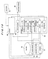
FIG. 12 is a diagram showing an example of an
arrangement of a substrate processing apparatus;
FIG. 13 is a diagram showing an example of a flow
of substrates between processing devices in the substrate
processing apparatus shown in FIG. 12;
FIGS. 14A and 14B are diagrams showing an order of
substrates to be scheduled in FIG. 13;
FIG. 15 is a diagram showing an example of a flow
of substrates between processing devices in the substrate
processing apparatus shown in FIG. 12;
FIGS. 16A and 16B are diagrams showing an order of
substrates to be scheduled in FIG. 15;
FIG. 17 is a diagram showing an example of an
arrangement of a substrate processing apparatus;
FIG. 18 is a diagram showing an example of a flow
of substrates between processing devices in the substrate
processing apparatus shown in FIG. 17;
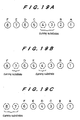
FIGS. 19A through 19C are diagrams showing an order
of substrates to be scheduled in FIG. 18;
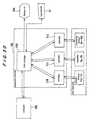
FIG. 20 is a block diagram showing an overall
arrangement of a substrate processing apparatus incorporating
a substrate transfer controlling apparatus according to the
present invention;
FIG. 21 is a diagram showing the scheduled result
obtained by scheduling execution times of transfer devices
with use of a substrate transfer controlling apparatus
according to the second embodiment of the present invention,
immediately after the substrate transfer controlling apparatus
has started to operate; and
FIG. 22 is a diagram showing the scheduled result
obtained by scheduling execution times of transfer devices
with use of a substrate transfer controlling apparatus
according to the second embodiment of the present invention,
after elapse of a certain time from the start of operation of
the substrate transfer controlling apparatus.
Best Mode for Carrying Out the Invention
A substrate transfer controlling apparatus
according to a first embodiment of the present invention will
be described below with reference to FIGS. 1 through 4. The
substrate transfer controlling apparatus according to the
present invention serves to control the transfer of substrates
between a plurality of processing devices installed in a
substrate processing apparatus. The substrate processing
apparatus in which the transfer of substrates is controlled by
the substrate transfer controlling apparatus will hereinafter
be described as a semiconductor fabrication apparatus for
processing semiconductor substrates (wafers). However, the
present invention is not limited to the semiconductor
fabrication apparatus, but is also applicable to a substrate
processing apparatus for processing glass substrates for LCD
fabrication, for example.
FIG. 1 is a schematic diagram showing an
arrangement of a semiconductor fabrication apparatus according
to the present embodiment. As shown in FIG. 1, the
semiconductor fabrication apparatus which is controlled by the
substrate transfer controlling apparatus according to the
present invention comprises transfer devices 1a through 1c for
transferring substrates, cassettes 2a, 2b which are loaded
with substrates, temporary stages 3a, 3b for use in receiving
and delivering substrates, an inverter 4, water cleaning and
drying devices 5a, 5b, chemical cleaning devices 6a, 6b, a
rough cleaning device 7, preprocessing tanks 8a, 8b, and
plating tanks 9a through 9d. In the present embodiment, not
only the processing components 5a through 9d, but also the
temporary stages 3a, 3b and the inverter 4 are handled as
processing devices. The semiconductor fabrication apparatus
may be arranged as any of various apparatus such as a CVD
apparatus for performing film deposition and a polishing
apparatus for polishing substrates, and the processing devices
may comprise various devices in accordance with the
semiconductor fabrication apparatus.
A substrate loaded in the cassette 2a or 2b is
introduced into the semiconductor fabrication apparatus by the
transfer device 1a, transferred to the temporary stage 3a by
the transfer device 1a, and further transferred to the
temporary stage 3b by the transfer device 1b. Then, the
substrate is transferred to the preprocessing tank 8a or 8b by
the transfer device 1c, processed therein, and then reversed.
Thereafter, the substrate is transferred to the plating tanks
9a through 9d by the transfer device 1c, processed therein,
and further transferred to the rough cleaning device 7. After
being roughly cleaned, the substrate is transferred to the
chemical cleaning device 6a or 6b by the transfer device 1b,
processed thereby, further transferred to the inverter 4, and
reversed thereby. The substrate is finally transferred to the
water cleaning and drying device 5a or 5b by the transfer
device 1a, processed thereby, and returned to the cassette 2a
or 2b which was initially loaded with the substrate. Not only
a single substrate may be processed at a time, but also a set
of a plurality of substrates held together which are
interconnected by a jig, for example, may be processed at a
time.
In the present embodiment, the actions of the
transfer devices 1a through 1c are predefined. For example,
predefined actions of the transfer device 1c include an action
C for moving to the temporary stage 3b and receiving a
substrate therefrom, an action D for transferring a substrate
to the preprocessing tanks 8a, 8b and delivering the substrate
thereto, an action E for moving to the preprocessing tanks 8a,
8b and receiving a preprocessed substrate therefrom, an action
F for transferring a substrate to the plating tanks 9a through
9d and delivering the substrate thereto, and an action G for
moving to the plating tanks 9a through 9d, receiving a plated
substrate therefrom, moving to the rough cleaning device, and
delivering the substrate thereto.
The substrate transfer controlling apparatus in the
present embodiment will be described below. FIG. 2 is a
diagram showing an example of a hardware configuration of the
substrate transfer controlling apparatus according to the
present embodiment, and FIG. 3 is a block diagram showing a
configuration of the substrate transfer controlling apparatus
according to the present embodiment.
As shown in FIG. 2, the substrate transfer
controlling apparatus 10 comprises a central processing unit
(CPU) 11, an input device 12 such as a pointing device
including a keyboard, a mouse, and the like, and a
communication device for reading data stored in other
computers, and storage devices including a ROM 13, a memory
14, and a hard disk 15. The substrate transfer controlling
apparatus 10 is connected to the transfer devices 1a through
1c of the semiconductor fabrication apparatus via an
input/output interface 16. Signals from the CPU 11 are
transmitted through the input/output interface 16 to the
transfer devices 1a through 1c of the semiconductor
fabrication apparatus for thereby controlling the transfer
devices 1a through 1c.
The ROM 13 and the hard disk 15 store the codes of
a computer program for issuing commands to the CPU 11 or the
like in cooperation with an operating system (OS) to control
the transfer of substrates. The computer program is loaded
into the memory 14 and executed in cooperation with the CPU 11
for performing the following substrate transfer controlling
process. The computer program in cooperation with the CPU 11
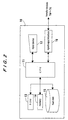
provides, as shown in FIG. 3, a schedule calculator 21, a
solution judging unit 22, a timetable generator 23, an action
commander 24, and a retrying unit 25. The hard disk 15 (or
the memory 14) stores a timetable 17 generated (updated) by
the timetable generator 23 described later.
A substrate transfer controlling process performed
by the substrate transfer controlling apparatus 10 will be
described below. FIG. 4 is a flowchart showing the substrate
transfer controlling process performed by the substrate
transfer controlling apparatus 10 according to the present
embodiment.
Before the substrate processing apparatus starts to
operate, times required for actions of the transfer devices 1a
through 1c in the semiconductor fabrication apparatus
(hereinafter referred to as "expected action times") are
inputted (Step 1). For example, an expected time required for
the transfer devices 1a through 1c to receive substrates from
processing devices, and an expected time required for the
transfer devices 1a through 1c to move from a processing
device to another processing device are inputted. The
expected action times are inputted with the input device 12.
Times required for processing substrates in the
processing devices 3a through 9d (hereinafter referred to as
"expected processing times") are inputted (Step 2). For
example, an expected time required to clean a substrate in the
rough cleaning device 7 is inputted. The expected processing
times are also inputted with the input device 12.
The input device for inputting the expected action
times and the expected processing times is not limited to a
keyboard, a pointing device, and the like. For example, the
expected action times and the expected processing times may be
prestored as a file in the storage device 14 or 15, and may
then be inputted by reading the file. Alternatively, such a
file may be saved in another computer, and the expected action
times and the expected processing times may be inputted by
reading the file through a communication device. For storing
expected action times as a file, times actually required for
the actions of transfer devices may be measured by a computer
connected to the transfer devices, and may be stored as
expected action times in a file. In this case, by measuring
times required for the actions of transfer devices while the
apparatus is being in operation, performing averaging or the
like, and then updating the expected action times stored in
the file, the accuracy of expected action times can be
increased, and the apparatus can cope with time-dependent
changes thereof.
Next, the schedule calculator 21 derives action
times of the actions of the transfer devices 1a through 1c
(hereinafter referred to as "execution times") for allowing
the time when a final one of the substrates to be processed is
fully processed and returned from the semiconductor
fabrication apparatus to be earliest (Step 3). The schedule
calculator 21 derives execution times by calculating a
solution satisfying a certain conditional formula, and the
details of this process will be described later.
A solution satisfying the above certain conditional
formula may not necessarily be derived. After calculations
carried out by the schedule calculator 21, the solution
judging unit 22 determines whether or not a solution
satisfying the above certain conditional formula has been
obtained (Step 4).
If the solution judging unit 22 determines that a
solution satisfying the above certain conditional formula has
been obtained, then the timetable generator 23 generates
(updates) a timetable 17 based on the execution times, i.e., a
timetable in which the obtained execution times are associated
with the actions of the transfer devices that are to be
performed at the execution times, and stores the timetable 17
in the hard disk 15 (Step 5).
When the semiconductor fabrication apparatus is in
operation, the action commander 24 controls the transfer
devices 1a through 1c by referring to the timetable 17 stored
in the hard disk 15. Specifically, the action commander 24
transmits a command for an action of the corresponding
transfer device through the input/output interface 16 to the
transfer device at an execution time described in the
timetable 17. As a result, the time when a final one of the
substrates to be processed is fully processed and returned
from the semiconductor fabrication apparatus is made earliest.
Before the action commander 24 transmits a command for an
action of each of the transfer devices 1a through 1c, the
action commander 24 confirms that the transfer device is
inoperative, and that the processing of a substrate in the
processing device as a transfer source is completed, and that
no preceding substrate is present in the processing device as
a transfer destination and the resetting of the processing
device is completed. If these conditions are not satisfied,
then the action commander 24 waits until the conditions are
satisfied and thereafter transmits a command.
If the solution judging unit 22 determines that a
solution satisfying the above certain conditional formula has
not been obtained, then the retrying unit 25 corrects the
conditional formula so as to reduce the average number of
substrates which are simultaneously present on the transfer
devices and the processing devices in the apparatus, i.e., by
adjusting intervals at which substrates are introduced, and
retries the processes from Step 3 (Step 6). The conditional
formula is corrected by inserting a virtual substrate
(hereinafter referred to as "dummy substrate") for which the
expected action times of the transfer devices and the expected
processing times of the processing devices are zero, at a
suitable interval between substrates. At this time, if the
number of the substrates that are simultaneously present in
the apparatus is reduced, then the frequency of the actions of
the transfer devices is reduced and hence the transfer devices
can be operated more freely, so that the probability that a
solution will be obtained is increased. If no solution is
obtained even after the retrying unit 25 retries the process,
then the conditional formula is further corrected to reduce
the number of the substrates which are simultaneously present
in the apparatus. In extreme cases, after a preceding
substrate is fully processed and returned to the cassette 2a
or 2b, a next substrate is introduced into the apparatus.
Next, the setting of a conditional formula and the
deriving of the execution times in the schedule calculator 21
will be described below with a specific example. The setting
of a conditional formula and the deriving of the execution
times which will be described below are examples thereof, and
can be performed according to any of all other processes.
First, the numbers (action numbers) k of actions of
the transfer devices 1a through 1c are defined successively as
1, 2, 3, ···, K along a path from the introduction of a
substrate into the semiconductor fabrication apparatus to the
return of the substrate from the semiconductor fabrication
apparatus. It is assumed that a sufficient time has elapsed
from the start of operation of the semiconductor fabrication
apparatus and the semiconductor fabrication apparatus is in
steady operation with a sufficient number of substrates
present therein, and the number of a next action to be
executed by a transfer device performing an action k is
represented by kp(k). It is also assumed that a suitable
number of dummy substrates are present before the first
substrate at the start of operation of the semiconductor
fabrication apparatus and after the final substrate at the end
of operation of the semiconductor fabrication apparatus, with
the substrate number n being determined in the order in which
substrates including the dummy substrates are introduced from
the cassette 2a or 2b into the semiconductor fabrication
apparatus, and an increment in the substrate number of
substrates to be handled when the action k changes to the next
action kp(k) is represented by np(k). For example, with
regard to the semiconductor fabrication apparatus shown in
FIG. 1, the actions are defined as follows:
An action A of the transfer device 1a to transfer a
substrate loaded in the cassette 2a or 2b to the temporary
stage 3a is defined as k=1, an action B of the transfer device
1b to transfer a substrate on the temporary stage 3a to the
other temporary stage 3b is defined as k=2, the action C of
the transfer device 1c to move to the temporary stage 3b and
receive a substrate therefrom is defined as k=3, the action D
of the transfer device 1c to transfer the received substrate
to the preprocessing tank 8a or 8b and deliver the substrate
thereto is defined as k=4, the action E of the transfer device
1c to move to the preprocessing tank 8a or 8b and receive the
substrate therefrom is defined as k=5, the action F of the
transfer device 1c to transfer the received substrate to the
plating tanks 9a through 9d and deliver the substrate thereto
is defined as k=6, and the action G of the transfer device 1c
to move to the plating tanks 9a through 9d, receive a plated
substrate therefrom, move to the rough cleaning device 7, and
deliver the substrate thereto is defined as k=7.
On the assumption that a sufficient time has
elapsed from the start of operation of the semiconductor
fabrication apparatus and the semiconductor fabrication
apparatus is in steady operation with a sufficient number of
substrates present therein, a sequence of actions of the
transfer devices is determined. For example, a sequence of
actions of the transfer device 1c is defined as a periodic
sequence of 3 → 5 → 4 → 6 → 7 → 3 → ··· in terms of the
action numbers. In this example, next actions are represented
as follows:
kp(3) = 5
kp(4) = 6
kp(5) = 4
kp(6) = 7
kp(7) = 3
The increments np in the substrate number when the action k
changes to the next action kp(k) are defined as shown below.
The increments np are determined in view of the number of each
type of the processing devices 3a through 9d.
np(3) = - 2
np(4) = - 2
np(5) = + 2
np(6) = - 3
np(7) = + 6
If each of substrates is assigned periodically in
an introduced sequence to the processing devices of the same
type (e.g., 8a and 8b, 9a through 9d), then expected action
times are uniquely determined as shown below. These expected
action times are inputted with the
input device 12 or
calculated in view of the positions and paths of the transfer
devices based on the inputted values.
These expected action times may occasionally be
zero.
The sum of the above expected action times is
defined as Tg(k, n). Specifically,
Tg(k, n) = M1(k, n) + G1(k, n)
+ M(k, n) + G2(k, n) + M2(k, n)
The following non-negative variables are defined:
The waiting time xw(k, n) is defined only with
respect to actions including the reception of the substrate
from the processing device. The idle time xf(k, n) is defined
only with respect to actions including the delivery of the
substrate to the processing device. Practically, however, the
idle time xf(k, n) may be limited to actions to deliver the
substrate to a relay-type processing device which is used to
receive and deliver substrates between transfer devices.
If the time to start an action k on a substrate n
is represented by t(k, n), then the following three equations
are established.
t(kp(k), n+np(k))
= t(k, n) + Tg(k, n)
+ xr(kp(k), n+np(k))
t(k+1, n)
= t(k, n) + Tg(k, n) - M2(k, n) + P(k, n)
- M1(k+1, n) + xw(k+1, n)
t(k, n)
= t(k+1, n-U(k))
+ M1(k+1, n-U(k)) + G1(k+1, n-U(k))
- M1(k, n) - G1(k, n) - M(k, n) + xf(k, n)
P(k, n) in the equation (2) represents an expected
processing time of the substrate number n after an action
indicated by the action number k, which is either inputted
with the input device 12 or calculated based on inputted
values. The expected processing time P(k, n) includes, in
addition to a time for plating, cleaning, or the like, which
is normally specified for each of substrates, a time required
for pre-actions such as shutter closing and liquid filling
performed before the substrate is processed by the processing
device, and a time required for post-actions such as liquid
removal and shutter opening performed after the substrate is
processed by the processing device. U(k) in the equation (3)
represents the number of processing devices of one type to
which the substrate is delivered by the action k.
The equation (1) represents a time to start an
action to be carried out by the same transfer device next
after the action k on the substrate n. The equation (2)
represents a time to start an action k+1 to be carried out
next after the substrate n is processed by the processing
device. The equation (3) represents a time to start an action
of the transfer device to deliver the next substrate n after
having received the processed substrate from the processing
device.
The equations (1) through (3) can be modified as
follows:
T = Rm Xr + Rv
Xw = Wm Xr + Wv
Xf = Fm Xr + Fv
where T, Xr, Xw, Xf represent column vectors having t(k, n),
xr(k, n), xw(k, n), xf(k, n) as respective elements, and Rm,
Wm, Fm represent suitable matrixes, and Rv, Wv, Fv represent
suitable column vectors.
The vector T on the left side of the equation (1a)
contains an element corresponding to t(K, N) which represents
a time to start an action to return the final substrate N
(except for a dummy substrate). If a corresponding element in
the vector Rm Xr on the right side of the equation (1a) is
minimum, then the time when the final substrate to be
processed is fully processed and returned from the
semiconductor fabrication apparatus is made earliest.
The condition for allowing the time for returning
substrates to be earliest can be expressed as follows:
cXr → minimum
where c represents a suitable row vector.
The conditions under which the transfer actions
represented by the above equations (1a) through (3a) are
physically established are normally indicated by Xr≧0, Xw≧0,
Xf≧0. From these inequalities and the above equations (1a)
through (3a), there can be derived the following inequalities:
Xr ≧ 0
Wm Xr ≧ -Wv
Fm Xr ≧ -Fv
If a certain time is required from the reception of
a preceding substrate from a processing device by a transfer
device until the delivery of a next substrate to the
processing device by a transfer device, then the required time
is added to the corresponding element on the right side of the
inequality (3b). For example, after the transfer device 1a
receives a reversed substrate from the inverter 4, the
transfer device 1b can deliver a next substrate to the
inverter 4 only when the reversing mechanism of the inverter 4
is reset. In this case, a time required to reset the
reversing mechanism is added to the corresponding element on
the right side of the inequality (3b).
As indicated by the equation (1a), since all the
times to start actions are expressed by a linear expression of
Xr, a linear constraint in relation to an arbitrary action
time can be expressed by a linear inequality relative to Xr.
For example, if the constraint is such that a substrate
immediately after it has been processed is immediately
received by an action k0, i.e., if xw(k0, n)=0, then the row
corresponding to k0 in the equation (2a) is taken out and can
be expressed by the following linear inequality.
-Wm0 Xr0 ≧ Wv0
If a constraint is given to provide an upper limit
for the time from the reception of a substrate n0 from an
immediately prior processing device in an action k0 until the
delivery of the substrate n0 to a next processing device in an
action k0+1, then an inequality of a similar form can be
derived. Similarly, it is possible to give a constraint to
provide a lower limit between times to start two actions, for
thereby scheduling the transfer devices with a certain time
allowance. Furthermore, it is also possible to define a
waiting time from the delivery of a substrate n to a
processing device in an action k until the start of an actual
process on the substrate n as xww(k, n), and formulate it so
as to be included in the above variable vector Xr. In this
case, the probability satisfying a constraint to provide an
upper limit for xw(k+1, n) can be increased.
The inequalities (1b) through (3b) and (5) can be
expressed as follows:
AXr ≧ b
where A represents a suitable matrix and b represents a
suitable column vector.
Therefore, in order to allow the time to return the
final substrate to be earliest, it is necessary to determine a
minimum value of the equation (4) under the inequality (6).
Such a solution Xr can be obtained as a solution to a problem
of a linear programming process. Once the solution Xr is
obtained, the execution times of respective actions for
allowing the time to return the final substrate to be earliest
can be obtained from the equation (1a), and the above
timetable can be generated (updated) based on the obtained
execution times.
A substrate transfer controlling apparatus
according to a second embodiment of the present invention will
be described below with reference to FIGS. 5 through 7. FIG.
5 is a block diagram showing a configuration of the substrate
transfer controlling apparatus 10 according to the present
embodiment, FIG. 6 is a flowchart showing a substrate transfer
controlling process carried out by the substrate transfer
controlling apparatus 10 according to the present embodiment,
and FIG. 7 is a diagram showing a visual representation of a
time domain to be scheduled according to the present
embodiment.
For operating a semiconductor fabrication apparatus
continuously for a long period of time, expected processing
times for substrates may not necessarily be predetermined, but
expected processing times may be determined for unprocessed
substrates in a cassette while the semiconductor fabrication
apparatus is in operation, e.g., each time a new cassette is
loaded, and the transfer of the substrates may be controlled
based on those expected processing times. The substrate
transfer controlling apparatus according to the second
embodiment can cope with such a situation.
Specifically, the substrate transfer controlling
apparatus 10 according to the present embodiment shifts a time
domain to be scheduled as shown in FIG. 7 backward during
operation of the semiconductor fabrication apparatus, repeats
the scheduling successively, and joins the results of
respective scheduling events consistently for controlling the
transfer of the substrates.
As shown in FIG. 5, the substrate transfer
controlling apparatus 10 according to the present embodiment
has a calculation time table 18 stored in the hard disk 15. A
computer program stored in the storage devices 13 through 15
in cooperation with the CPU 11 provides a schedule judging
unit 31, a calculating condition determiner 32, a schedule
calculator 33, a solution judging unit 34, a timetable
generator 35, an action commander 36, and a retrying unit 37.
A substrate transfer controlling process carried
out by the substrate transfer controlling apparatus according
to the present embodiment will be described below.
As with the first embodiment, expected action times
are inputted with the input device 12 (Step 21), and expected
processing times are inputted with the input device 12 (Step
22). In the second embodiment, data inputted with the input
device are temporarily stored in the storage device 14 or 15,
and then read to enter expected action times and expected
processing times.
After the expected action times and the expected
processing times are inputted, the schedule judging unit 31
determines whether or not a new scheduling process is required
(Step 23), i.e., determines whether there is a substrate that
has not scheduled yet even though expected processing times
have been inputted.
If the schedule judging unit 31 judges that there
is no substrate that has not scheduled yet, i.e., no new
scheduling process is required, then the process returns to
Step 22 and waits for expected processing times to be
inputted.
If the schedule judging unit 31 judges that there
is a substrate that has not scheduled yet, then the
calculating condition determiner 32 determines an assumed time
subsequent to the present time and a final substrate (except
for a dummy substrate) to be subject to scheduling
calculations (Step 24). The final substrate is a final one of
new substrates to be subject to scheduling calculations, which
are added to the substrates which have already been scheduled,
and is not a dummy substrate.
The assumed time and the final substrate are
determined as follows: In the results of a past scheduling
process, as shown in FIG. 7, the time when a substrate
including a dummy substrate is first returned to the cassette
2a or 2b after a final non-dummy substrate (which is not a
dummy substrate) has been introduced into the semiconductor
fabrication apparatus is regarded as an assumed time. The
number of additional substrates in a range where scheduling
calculations therefor can be completed with an allowance from
the present time to the assumed time is presumed, and thus a
final one of the additional substrates is determined. The
number of additional substrates is presumed with the range of
substrates which have not been scheduled yet but for which
expected processing times have been inputted. If no positive
number of additional substrates is obtained, then the assumed
time is shifted to the returning time of a next scheduled
substrate, and the number of additional substrates is
determined. In this manner, the interval from the assumed
time to the time at which the final substrate is returned
represents an approximate time domain to be scheduled, as
shown in FIG. 7.
Here, the average value of times required to
perform scheduling calculations on added substrates is saved
as the calculation time table 18 in the hard disk 15. The
calculating condition determiner 32 estimates a suitable
number of added substrates in view of the times required for
calculations which are saved in the calculation time table 18.
The time to return the final substrate according to
the new scheduling process is usually later than a true
earliest value (earliest time) which is achieved when the
expected processing times of all substrates are given in
advance. If the number of substrates added in each scheduling
process is set to a relatively large value, then the time to
return the final substrate according to the new scheduling
process can be approximated to the true earliest value.
After the calculating condition determiner 32 has
determined an assumed time and a final substrate to be subject
to scheduling calculations, the schedule calculator 33 derives
execution times of the actions of the transfer devices within
the above time domain to be scheduled based on the conditional
formula after the above additional substrates have been added
(Step 25).
A lower limit for substrate numbers to be noticed
for each action k is determined by referring to a set of
action numbers of which execution times are subsequent to the
assumed time and substrate numbers in the results of the past
scheduling process. Alternatively, a lower limit for
substrate numbers may be determined by determining actions
which can happen subsequent to the assumed time due to the
order of actions of the transfer devices depending on expected
processing times and expected action times. In this manner,
the execution times of most actions prior to the assumed time
are held, and the execution times of some actions may not be
held in the vicinity of the assumed time, in the results of
the past scheduling process.
Further, an upper limit for substrate numbers is
determined by determining actions which can happen prior to
the time to start the returning action of the final substrate
to be subject to the above scheduling calculations to the
cassette. It is assumed that dummy substrates of which action
times and processing times are zero exist subsequent to the
final substrate.
Based on the lower limit and the upper limit thus
determined for substrate numbers, unknown column vectors T,
Xr, and the like are constructed, and scheduling calculations
are carried out. In each of scheduling calculations, the
average value of times required for scheduling calculations,
which has been saved in the calculation time table 18, is
updated based on the times that are actually required for the
calculations.
When the semiconductor fabrication apparatus starts
continuous operation, the immediacy of scheduling is
particularly important. Therefore, action times are
determined in the order of actions k = 1, 2, ···, K as minimum
values satisfying the equations (1) through (3) with respect
to the first substrate. If a single substrate is processed in
the semiconductor fabrication apparatus, then the action times
thus determined allow the time to return the substrate to be
earliest. Unless expected processing times and expected
action times have extreme values, the substrate is processed
by each of the processing devices 3a through 9d and then
immediately transferred to the next processing device by the
transfer devices 1a through 1c. Thus, an optimum solution
satisfying the given constraint is determined.
After the schedule calculator 33 has performed its
processing operation, as with the first embodiment, the
solution judging unit 34 determines whether or not a solution
of execution times has been obtained (Step 26). If a solution
of execution times has been obtained, then the timetable
generator 35 generates (updates) a timetable (Step 27). After
the timetable has been generated (updated), the process
returns to Step 22, and the subsequent steps are repeated.
The action commander 36 refers to the timetable 17
stored in the hard disk 15 to control the transfer devices 1a
through 1c, as with the first embodiment.
On the other hand, if the solution judging unit 34
judges that a solution of execution times has not been
obtained, then the retrying unit 37 inserts a dummy substrate
between substrates (Step 28), as with the first embodiment.
In this case, the calculating condition determiner 32
determines an assumed time and a final substrate to be subject
to scheduling calculations such that a non-dummy additional
substrate will exist, also in view of the inserted dummy
substrate.
In the present embodiment, since the execution
times of actions of the transfer devices which are determined
by the new scheduling process may possibly be prior to the
assumed time, it is necessary to set a margin of safety to a
large value in presuming the number of additional substrates
for finishing scheduling calculations earlier than the assumed
time to allow the action commander 36 to issue action commands
to the transfer devices.
A substrate transfer controlling apparatus
according to a third embodiment of the present invention will
be described below with reference to FIGS. 8 and 9. FIG. 8 is
a block diagram showing a configuration of the substrate
transfer controlling apparatus 10 according to the present
embodiment.
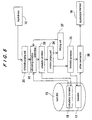
As shown in FIG. 8, the substrate transfer
controlling apparatus 10 according to the third embodiment
comprises a scheduler 40, a schedule corrector 50, and an
action commander 60, and has a progress data file 19 stored in
the hard disk 15. The action commander 60 corresponds to the
action commander 36 according to the second embodiment.
The scheduler 40 is constituted by the schedule
judging unit, the calculating condition determiner, the
schedule calculator, the solution judging unit, the timetable
generator, the action commander, and the retrying unit
according to the second embodiment. The schedule corrector 50
comprises an actual time acquisition unit 51, a rescheduling
judging unit 52, an invalidating unit 53, a progress data
acquisition unit 54, a corrector 55, and a validating unit 56.
The scheduler 40 and the schedule corrector 50 are provided by
a computer program stored in the storage devices 13 through 15
in cooperation with the CPU 11.
A substrate transfer controlling process carried
out by the substrate transfer controlling apparatus according
to the present embodiment will be described below. FIG. 9 is
a flowchart of a process carried out by the schedule corrector
50 in the substrate transfer controlling apparatus according
to the present embodiment.
The basic process carried out by the scheduler 40
is the same as the aforementioned process according to the
second embodiment, but differs therefrom in that the
conditional data including expected action times and expected
processing times, the times t(k, n), xr(k, n), and the data of
scheduling results such as the scheduled final substrate
number and the like are shared as the progress data file 19
with the schedule corrector 50 and updated consistently.
Specifically, when the semiconductor fabrication
apparatus starts operation, expected action times of the
individual transfer devices are inputted with the input device
12, and stored as the progress data file 19 in the memory 14
or the hard disk 15. After the semiconductor fabrication
apparatus starts continuous operation, when expected
processing times of each type of the processing devices for
substrates are inputted with the input device 12, these
expected processing times are also stored as the progress data
file 19 in the memory 14 or the hard disk 15. Thereafter, in
order to reflect the execution times of actions of the
transfer devices as corrected by the schedule corrector 50,
the progress data file 19 is read, and the process is carried
out up to the step of generating (updating) the timetable 17
with the timetable generator based on the progress data file
19. The results are accumulated in the progress data file 19.
The data accumulated in the progress data file 19 which are
old and unnecessary are successively deleted at respective
times by referring to the numbers of substrates actually fully
processed and returned to the cassette.
When the schedule judging unit is to determine
whether new scheduling calculations are necessary and when the
calculating condition determiner is to determine a final
substrate, a limitation may be posed on the range of
substrates to be subject to scheduling calculations in view of
the storage capacity for the progress data file 19 and the
frequency of time corrections.
In the present embodiment, the schedule corrector
50 performs the following process independently of the above
process carried out by the scheduler 40.
The actual time acquisition unit 51 acquires times
(hereinafter referred to as "actual times") at which the
transfer devices 1a through 1c actually start their actions,
via the input/output interface 16 (Step 41). Then, the
rescheduling judging unit 52 determines the difference between
the actual times acquired by the actual time acquisition unit
51 and the execution times scheduled in the past and described
in the timetable 17, and determines whether or not the
difference exceeds a predetermined allowable range (Step 42).
If the above delay time does not exceed the
allowable range, then the actual time acquisition unit 51
acquires actual times again (Step 41). On the other hand, if
the above delay time exceeds the allowable range, then the
execution times described in the timetable 17 need to be
corrected. Therefore, a process described below is performed
(Steps 43 through 47). The rescheduling judging unit 52 may
determine whether or not actions are inconsistent in relation
to the actual times and the execution times described in the
timetable 17. For example, when an action of a transfer
device is delayed and another transfer device is scheduled to
receive a substrate from a relay-type processing device before
the above transfer device actually delivers a substrate to the
relay-type processing device, such actions are inconsistent,
and hence the execution times may be corrected.
When the actual time acquisition unit 51 is to
acquire actual times, the actual time acquisition unit 51 may
acquire, in addition to the times when the transfer devices
start to perform their actions, data representing the progress
of the actions, e.g., times to move to processing devices as
transfer sources and transfer destinations, times to end
receiving and delivering substrates, and times to end
processing in processing devices, for correcting execution
times with higher accuracy.
The Steps 43 through 47 are carried out as follows:
The invalidating unit 53 invalidates or stops the process of
the scheduler 40 (Step 43), and the progress data acquisition
unit 54 acquires the progress data by referring to the
progress data file 19 (Step 44).
Then, the corrector 55 calculates new (corrected)
execution times which satisfy the above equations (1) through
(3), as minimum values not smaller than the times scheduled in
the past, for actions that are not performed at present, with
respect to substrates (including dummy substrates) present on
the transfer devices and the processing devices in the
semiconductor fabrication apparatus and a single first
substrate (including a dummy substrate) to be introduced into
the semiconductor fabrication apparatus, based on the progress
data and the actual times inputted by the actual time
acquisition unit 51 (Step 45). At this time, the final
substrate which has been scheduled is the single first
substrate to be introduced into the semiconductor fabrication
apparatus, and a suitable number of dummy substrates are
inserted subsequent to the final substrate for calculation
purposes. The corrector 55 then updates the timetable 17 and
the progress data file 19 based on the corrected execution
times (Step 46).
In calculating the above new execution times, for
the sake of brevity, the times scheduled in the past may be
shifted altogether back in timed relation to a delay in the
latest actual time. The time for a transfer device to end
receiving a substrate from a processing device as a transfer
source or the time for a transfer device to end delivering a
substrate to a processing device as a transfer destination may
be compared with the results of the past scheduling process.
Thereafter, the validating unit 56 validates or
resumes the process of the scheduler 40 which has been
invalidated or stopped by the invalidating unit 53 (Step 47).
After being validated or resumed, the scheduler 40 performs
its process based on the updated data in the progress data
file 19.
If an action of a transfer device is delayed later
than expected, the constraint relative to the action times of
the transfer device being considered is not necessarily
satisfied. Any deviation from the constraint can be reduced
to a negligible level by setting a delay reference in the
rescheduling judging unit 52 to an appropriate value. After
the process of the scheduler 40 has been validated or resumed,
it is possible to determine an optimum value in the view of a
constraint according to a linear programming process with
respect to subsequent substrates, thus eliminating the effect
of a time delay in the future.
A substrate transfer controlling apparatus
according to a fourth embodiment of the present invention will
be described below with reference to FIGS. 10 and 11. FIG. 10
is a block diagram showing a configuration of the substrate
transfer controlling apparatus 10 according to the present
embodiment.
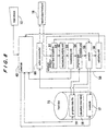
As shown in FIG. 10, the substrate transfer
controlling apparatus 10 according to the present embodiment
comprises a scheduler 40, a schedule corrector 70, and an
action commander 60, and has a progress data file 19 stored in
the hard disk 15. The scheduler 40 and the schedule corrector
70 are provided by a computer program stored in the storage
devices 13 through 15 in cooperation with the CPU 11. The
schedule corrector 70 in the present embodiment is constituted
by a condition change detector 71, an invalidating unit 72, a
progress data acquisition unit 73, an expected processing time
updater 74, a corrector 75, and a validating unit 76.
The process performed by the scheduler 40 is the
same as the process described above in the second and third
embodiments. The schedule corrector 70 performs a process
which is different from the process carried out by the
schedule corrector 50 according to the third embodiment. The
process carried out by the schedule corrector 70 in the
present invention will be described below. The process
carried out by the schedule corrector 70 is performed
independently of the process performed by the scheduler 40.
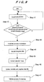
FIG. 11 is a flowchart of the process carried out by the
schedule corrector 70 according to the present embodiment.
After the semiconductor fabrication apparatus
starts to operate, the condition change detector 71 detects,
through the input device 12, whether there is a change in
conditions with respect to a substrate (hereinafter referred
to as "unintroduced substrate") expected to be introduced into
the semiconductor fabrication apparatus, e.g., a cancellation
of the introduction of an unintroduced substrate into the
semiconductor fabrication apparatus, a change in the expected
processing time of an unintroduced substrate, or a change in
the sequence of introduction of an unintroduced substrate into
the semiconductor fabrication apparatus (Step 51). If the
condition change detector 71 detects a change in conditions
with respect to an unintroduced substrate, then since
execution times described in the timetable 17 need to be
corrected, the following process is carried out.
The invalidating unit 72 invalidates or stops the
process of the scheduler 40 (Step 52), and the progress data
acquisition unit 73 acquires the progress data by referring to
the progress data file 19 (Step 53). The expected processing
time updater 74 refers to a change in the conditions with
respect to an unintroduced substrate (a cancellation of the
introduction of an unintroduced substrate into the
semiconductor fabrication apparatus, a change in the expected
processing time of an unintroduced substrate, or a change in
the sequence of introduction of an unintroduced substrate into
the semiconductor fabrication apparatus), and updates the data
regarding the expected processing times which has been
accumulated as part of the progress data (Step 54). For an
unintroduced substrate which has been changed in conditions, a
new introducing sequence is established, and the expected
processing times are updated based on the new introducing
sequence. If constraints relative to the transfer are
specified for individual substrates, then these constraints
are also updated.
If the first substrate for which expected
processing times have been updated in Step 54 has already been
scheduled in the past, then the corrector 75 cancels the
results of the scheduling process for the substrate and
subsequent substrates among the results of the past scheduling
process in the progress data, and inserts a suitable number of
dummy substrates. Then, the corrector 75 calculates new
(corrected) execution times which satisfy the above equations
(1) through (3), as minimum values not smaller than the times
scheduled in the past (Step 55). At this time, the final
substrate which has been scheduled is the final substrate for
which expected processing times have not been changed in Step
54. The corrector 75 then updates the timetable 17 and the
progress data file 19 based on the corrected execution times
(Step 56). The time for a transfer device to end receiving a
substrate from a processing device as a transfer source or the
time for a transfer device to end delivering a substrate to a
processing device as a transfer destination may be compared
with the results of the past scheduling process.
Thereafter, the validating unit 76 validates or
resumes the process of the scheduler 40 which has been
invalidated or stopped by the invalidating unit 72 (Step 57).
After being validated or resumed, the scheduler 40 performs
its process based on the updated data in the progress data
file 19. As a result, the execution times of actions on the
first substrate and subsequent substrates for which expected
processing times have been changed in Step 54 can be
recalculated based on the changed expected processing times.
Even when a change occurs in the conditions with respect to an
unintroduced substrate, such as a cancellation of the
introduction of an unintroduced substrate into the
semiconductor fabrication apparatus, a change in the expected
processing time of an unintroduced substrate, or a change in
the sequence of introduction of an unintroduced substrate into
the semiconductor fabrication apparatus, the substrate
processing apparatus can thus be operated flexibly based on
the change in the conditions.
The schedule corrector 70 according to the present
embodiment and the schedule corrector 50 according to the
third embodiment may be arranged so as to function
simultaneously with each other.
As described above, the schedule calculator in each
of the above embodiments derives the execution times of
actions of the transfer devices such that the time at which
the final substrate has been fully processed and returned from
the semiconductor fabrication apparatus is made earliest.
According to the present invention, even if a certain
substrate is instructed not to be processed by a certain
processing device, it is possible to calculate the execution
times of actions of the transfer devices to transfer the
substrate so as to skip the processing device instructed not
to process the substrate. The substrate may be instructed not
to be processed by the processing device by setting the
expected processing time in the processing device for the
substrate to zero.
For transferring the substrate to skip the
processing device, a suitable number of dummy substrates are
inserted immediately before the processing device to be
skipped and also immediately prior to the substrate. The
execution times are then calculated based on the above linear
programming process on the assumption of the inserted dummy
substrates. By thus inserting a suitable number of dummy
substrates, it is possible to transfer the substrate to skip
the processing device. Insertion of such dummy substrates
will be described below.
It is assumed that processing device types S1
through S3 are installed in a substrate processing apparatus,
as shown in FIG. 12. It is also assumed that actions k-1, k,
k+1 including the delivery of substrates to the processing
device types S1 through S3 are carried out by the same
transfer device, and that substrates A, B, C are introduced
into and transferred in and processed by the substrate
processing apparatus in the order named.
Here, a situation where the expected processing
time of the substrates B, C with the processing device type S2
is set to zero, and hence the substrates B, C are transferred
to skip the process in the processing device type S2 will be
considered. FIGS. 13 and 15 show examples of flows of
substrates between the processing device types shown in FIG.
12, with the time axis being directed downwardly.
In this case, as shown in FIG. 16A, a certain
number of dummy substrates which correspond to the number 2 of
processing devices of the processing device type S2 minus 1,
i.e., one dummy substrate 2 ○ is inserted immediately prior to
the substrate B. The action [k, 3] including the reception of
the substrate B (3 ○) from the processing device type S1 is
handled as an action on the dummy substrate, and the
processing device type as a transfer source for a next action,
i.e., the action [k+1, 2] on the dummy substrate 2 ○ , is
changed from S2 to S1. As a result, as indicated by the
dotted line in FIG. 15, the substrate B is transferred from
the processing device type S1 to the processing device type
S3.
Similarly, the action [k, 4] including the
reception of the substrate C (4 ○) from the processing device
type S1 is handled as an action on the dummy substrate, and
the processing device type as a transfer source for the action
[k+1, 3] on the dummy substrate 3 ○ is changed from S2 to S1.
As a result, as indicated by the dotted line in FIG. 15, the
substrate C is transferred from the processing device type S1
to the processing device type S3.
In this manner, the reception of the substrate B
from the processing device type S1 is completed before the
action [k-1, 4] including the delivery of the substrate C to
the processing device type S1, and the reception of the
substrate C from the processing device type S1 is also
completed before the action [k-1, 5] including the delivery of
the substrate D to the processing device type S1. Therefore,
the transfer device can transfer these substrates C, D to the
processing device type S1 without problems. The dummy
substrate which was present before the substrates B, C is
moved backward of the substrates B, C after the action [k+1,
3], as shown in FIG. 16B.
In the above description, one processing device
type is skipped, and the action k-1 is carried out by the same
transfer device as the actions k, k+1. For transferring a
substrate so as to skip a plurality of processing device
types, dummy substrates are inserted in view of all those
processing device types to be skipped to allow the substrate
to be transferred while skipping those processing device
types.
Even if the action k-1 is carried out by another
transfer device, an action of a transfer device for receiving
a substrate from and delivering a substrate to the other
transfer device via a relay-type processing device type is
taken into consideration instead of the action k-1, and the
number of dummy substrates to be inserted is determined so as
not to affect the action sequence of the other transfer device
for thereby making it possible to skip the processing transfer
device types.
Next, it is assumed that processing device types S1
through S4 are installed in a substrate processing apparatus,
as shown in FIG. 17. It is also assumed that actions k-1, k,
k+1, k+2 including the delivery of substrates to the
processing device types S1 through S4 are carried out by the
same transfer device, and that substrates A, B, C, D, E, F are
introduced into and transferred in and processed by the
substrate processing apparatus in the order named. It is
further assumed that the action sequence of the transfer
device is represented by k+2, k+1, k, k-1 during steady
operation of the substrate processing apparatus, and the
actions of the transfer device are performed in the order
shown in FIG. 18, with the time axis being directed downwardly
in FIG. 18.
Here, a situation where the substrates C, D are
transferred so as to skip the process in the processing device
type S3 and the substrates E, F are transferred so as to skip
the process in the processing device type S2 will be
considered.
In this case, as shown in FIG. 19A, a certain
number of dummy substrates which correspond to the number of
processing devices of the processing device type S3, i.e., two
dummy substrates 3 ○, 4 ○ are inserted immediately prior to the
substrate C. The processing device type as a transfer source
for the action [k+2, 3] on the dummy substrate 3 ○ is changed
from S3 to S2, and the action [k+2, 3] is carried out prior to
the action [k+1, 5] including the reception of the substrate C
(5 ○) from the processing device type S2. Thus, the substrate
C is transferred so as to skip the processing device type S3.
Further, the processing device type as a transfer
source for the action [k+1, 5] is changed from S2 to S1, and
the action [k+1, 5] is carried out prior to the action [k, 7]
including the reception of the substrate E (7 ○) from the
processing device type S1. Thus, the substrate E is
transferred so as to skip the processing device type S2. At
this time, one of the dummy substrates is moved backward of
the substrate D, as shown in FIG. 19B.
Similarly, the processing device type as a transfer
source for the action [k+2, 4] is changed from S3 to S2, and
the action [k+2, 4] is carried out prior to the action [k+1,
6] including the reception of the substrate D from the
processing device type S2. Thus, the substrate D is
transferred so as to skip the processing device type S3.
Furthermore, the processing device type as a
transfer source for the action [k+1, 6] is changed from S2 to
S1, and the action [k+1, 6] is carried out prior to the action
[k, 8] including the reception of the substrate F (8 ○) from
the processing device type S1. Thus, the substrate F is
transferred so as to skip the processing device type S2. At
this time, the two dummy substrates are moved backward of the
substrate F, as shown in FIG. 19C.
According to the present invention, since each of
substrates can be transferred so as to skip an unwanted
processing device type or types and a plurality of processing
device types can selectively be used depending on the purpose
of processes performed thereby while the substrate processing
apparatus is being continuously operated, the substrate
processing apparatus can flexibly be operated for multi-product
small-lot production. For example, the throughput can
be made much greater than that in the case where the
continuous operation is temporarily stopped and substrates to
be processed differently are handled. The cost can also be
made much lower than that in the case where different
substrate processing apparatuses are employed to serve
different processing purposes.
When the schedule calculator (denoted by the
reference numeral 21 in FIG. 3, the reference numeral 33 in
FIG. 5) is arranged in view of skipping processing device
types, the corrector (denoted by the reference numeral 55 in
FIG. 8, the reference numeral 75 in FIG. 10) is also arranged
in view of skipping processing device types.
A substrate processing apparatus incorporating a
substrate transfer controlling apparatus according to the
present invention will be described below with reference to
the accompanying drawings. FIG. 20 is a block diagram showing
an overall arrangement of a substrate processing apparatus
(semiconductor fabrication apparatus) according to the present
embodiment. The substrate processing apparatus has the
transfer devices 1a through 1c, the cassettes 2a, 2b, and the
processing devices 3a through 9d shown in FIG. 1 as a main
assembly. The substrate processing apparatus also has an
apparatus controller 110 comprising a computer or the like, a
scheduler 102 comprising an independent computer or the like,
a display unit 104 for displaying statuses of the apparatus,
and the aforementioned input device 12 for inputting operating
conditions and control conditions of the apparatus.
Storage devices in the apparatus controller 100 and
the scheduler 102 store a computer program for controlling
substrates and a computer program for controlling the
apparatus. The apparatus controller 100 and the scheduler 102
may be implemented by a plurality of computers in cooperation
with each other or a single computer.
The apparatus controller 100 mainly comprises
controllers 110 through 112 connected to the transfer devices
1a through 1c, the cassettes 2a, 2b, and the processing
devices 3a through 9d in the main assembly, and a main
controller 120 connected to the controllers 110 through 112.
The controllers 110 through 112 receive commands from the main
controller 120 and transmit the commands to the devices 1a
through 9d. The controllers 110 through 112 monitor the
devices 1a through 9d and transmit signals representative of
the statuses of the devices 1a through 9d to the main
controller 20. The main controller 120 has a function to
transmit starting commands, processing conditions, and the
like to the processing devices 3a through 9d, and also
includes an action commander (denoted by the reference numeral
24 in FIG. 3, the reference numeral 36 in FIG. 5, the
reference numeral 60 in FIGS. 8 and 10), an actual time
acquisition unit (denoted by the reference numeral 51 in FIG.
8), a rescheduling judging unit (denoted by the reference
numeral 52 in FIG. 8), and a condition change detector
(denoted by the reference numeral 71 in FIG. 10), all for
controlling the transfer devices. The display unit 104 and
the input device 12 are connected to the main controller 120.
The scheduler 102 includes a schedule calculator
(denoted by the reference numeral 21 in FIG. 3, the reference
numeral 33 in FIG. 5), a solution judging unit (denoted by the
reference numeral 22 in FIG. 3, the reference numeral 34 in
FIG. 5), a retrying unit (denoted by the reference numeral 25
in FIG. 3, the reference numeral 37 in FIG. 5), a timetable
generator (denoted by the reference numeral 23 in FIG. 3, the
reference numeral 35 in FIG. 5), a schedule judging unit
(denoted by the reference numeral 31 in FIG. 5), a calculating
condition determiner (denoted by the reference numeral 32 in
FIG. 5), an invalidating unit (denoted by the reference
numeral 53 in FIG. 8, the reference numeral 72 in FIG. 10), a
progress data acquisition unit (denoted by the reference
numeral 54 in FIG. 8, the reference numeral 73 in FIG. 10), a
corrector (denoted by the reference numeral 55 in FIG. 8, the
reference numeral 75 in FIG. 10), a validating unit (denoted
by the reference numeral 56 in FIG. 8, the reference numeral
76 in FIG. 10), and an expected processing time updater
(denoted by the reference numeral 74 in FIG. 10).
The above arrangements of the main controller 120
and the scheduler 102 are examples thereof, and the main
controller 120 and the scheduler 102 may of course be arranged
differently.
Operation of the substrate processing apparatus
incorporating the substrate transfer controlling apparatus
will be described below.
The power supply of the main assembly is ganged
with the power supplies of the apparatus controller 100, the
display unit 104, the input device 12, and the scheduler 102.
When the power supply of the main assembly is turned on, the
power supplies of the apparatus controller 100, the display
unit 104, the input device 12, and the scheduler 102 are
automatically turned on, for thereby activating the apparatus
controller 100, the display unit 104, the input device 12, and
the scheduler 102. At this time, the scheduler 102 is in a
standby state waiting for a signal from the main controller
120.
Before the main assembly is operated, information
as to whether the processing devices 3a through 9d are to be
used or not, a transferring path indicative of the sequence of
transfer of substrates between the types of the processing
devices 3a through 9d with the transfer devices 1a through 1c,
and the sequence of basic actions of the transfer devices 1a
through 1c in steady operation of the substrate processing
apparatus are inputted with the input device 12. The main
controller 120 may transmit action commands to the transfer
devices 1a through 1c in the main assembly to operate the
transfer devices 1a through 1c, and acquire times required for
the actions of the transfer devices 1a through 1c. If the
acquired times and other settings are stored in a magnetic
disk or a nonvolatile memory in the apparatus controller 100,
then the substrate processing apparatus can be operated based
on those acquired times and other settings even after the
power supply thereof is turned off.
When a starting command for operation of the
apparatus is inputted with the input device 12, the main
controller 120 instructs the devices to start their
processing, i.e., to return the transfer devices 1a through 1c
to their home positions and initialize the processing devices
3a through 9d, and also transmits an operation starting
command and data indicative of the transferring path, the
sequence of basic actions, and expected action times to the
scheduler 102. The scheduler 102 reads these data and
performs an initializing process such as a setting process of
its internal memory.
When the cassettes 2a, 2b loaded with unprocessed
substrates are mounted in the main assembly, expected
processing times for those unprocessed substrates and
constraints about the transfer of the unprocessed substrates
are inputted with the input device 12. These inputted data
are transmitted via the main controller 120 to the scheduler
102.
The scheduler 102 reads the data of the expected
processing times and the constraints, generates a timetable by
calculating execution times of the actions with respect to the
first substrate according to the above substrate transfer
controlling process, and transmits the generated timetable to
the main controller 120. Based on the timetable, the main
controller 120 starts the actions of the transfer devices and
the processes in the processing devices corresponding to the
actions of the transfer devices, and starts measuring the
execution times of the actions. When transmitting action
commands to the transfer devices 1a through 1c, the main
controller 120 confirms not only the passage of times
indicated in the timetable, but also that the transfer devices
are inoperative, the processing of substrates in processing
devices as transfer sources has been completed, and preceding
substrates are not present in processing devices as transfer
destinations and the resetting of those processing devices has
been completed. In this manner, no problem occurs even if the
action times of the transfer devices 1a through 1c, the
processing times of the processing devices 3a through 9d, and
the reset times deviate from expected times.
Simultaneously with transmitting the action
commands, the main controller 120 transmits the execution
times of the actions to the scheduler 120, and also transmits
information about the positions of the substrates and the
progress of the processes to the output device 104.
Subsequently, these status data of the main assembly are
continuously transmitted at suitable given intervals.
Then, the scheduler 102 sets a suitable number of
additional substrates with respect to the second and
subsequent substrates for which expected processing times have
initially been acquired, successively schedules the substrates
according to a linear programming process, and transmits an
updated timetable to the main controller 120. Prior to
transmitting such an updated timetable, the scheduler 120 may
transmit a command to stop the clock in the main controller
120 to inhibit new actions from being started, may transmit
only commands corresponding to unperformed actions in the
timetable, and then may restart the clock in the main
controller 120 after transmitting those commands. In view of
the storage capacity of the storage devices in the main
controller 120, the timetable may be stored and accumulated in
the storage devices in the scheduler 102, and a certain amount
of schedule with unperformed actions at first may periodically
be transmitted sequentially to the main controller 120
irrespective of the timing of scheduling calculations.
When a cassette loaded with new unprocessed
substrates is mounted in the main assembly, expected
processing times and constraints of the transfer thereof are
inputted in the same manner as described above. The inputted
data are transmitted from the main controller 120 to the
scheduler 102. The scheduler 102 reads these data,
accumulates them in the progress data file, and continues the
above successive scheduling according to the linear
programming process.
When expected action times have been calculated
with respect to all unintroduced substrates for which expected
processing times have been inputted, the scheduler 102 waits
until the expected processing time of a next unintroduced
substrate is inputted.
While the main assembly is being in operation, the
main controller 120 measures the execution times of respective
actions, and monitors any differences between the measured
times and the times indicated in the timetable. If the action
times of the transfer devices 1a through 1c the processing
times of the processing devices 3a through 9d, and the reset
times are delayed, then the execution time of a certain action
may be delayed as a result. In such a case, the rescheduling
judging unit in the main controller 120 transmits a time
correction command to the scheduler 102, which corrects the
execution time of the unperformed action to update the
timetable and transmits the updated timetable to the main
controller 120. The main controller 120 stops the clock
before transmitting the time correction command, and restarts
the clock after having received the timetable, so that the
corrected timetable and actual actions are consistent with
each other.
When the mounted cassette loaded with unprocessed
substrates is removed from the main assembly, or the expected
introduction of unintroduced substrates is canceled, or the
expected processing times thereof are changed, or the sequence
of introduction of unintroduced substrates into the main
assembly is changed with the input device 12, the information
indicative of the above event is transferred together with a
correction command for the unintroduced substrates from the
main controller 120 to the scheduler 102. The scheduler 102
updates a portion of the timetable, and transmits the updated
timetable to the main controller 120. As in the case of the
time correction command, the main controller 120 stops the
clock before a correction command for the unintroduced
substrates is transmitted to the scheduler 102, and restarts
the clock after having received the timetable.
When all the substrates loaded in the cassette
mounted in the main assembly have been fully processed and
returned to the cassette, the main controller 120 stops
checking whether or not there is a transmission from the
scheduler 102, performs an ending process such as a releasing
process of the memory, and returns to the state subsequent to
the activation. The scheduler 102 and the input device 12
also return to the state subsequent to the activation. In
this case, the transferring path, the sequence of basic
actions, and expected action times for a next cycle of
operation may be reset with the input device 12.
Alternatively, an operation starting command may be inputted
again with the same settings to resume the processing of
substrates for a cassette loaded with unprocessed substrates.
FIGS. 21 and 22 show examples of the scheduled
results obtained by scheduling execution times of transfer
devices using the substrate transfer controlling apparatus
according to the second embodiment. In FIGS. 21 and 22, the
numerals represent substrate numbers, solid lines sandwiched
by × corresponding to the transfer devices 1a through 1c
indicate that the transfer devices are in operation, and solid
lines sandwiched by * corresponding to the processing devices
3a through 9d indicate that the processing devices are
processing substrates.
FIG. 21 shows the scheduled results obtained
immediately after the substrate transfer controlling apparatus
has started to operate. It can be seen from FIG. 21 that the
transfer devices 1a through 1c have a large allowance at the
time immediately after the substrate transfer controlling
apparatus has started to operate.
FIG. 22 shows the scheduled results obtained in a
steady state after elapse of a certain time from the start of
operation of the substrate transfer controlling apparatus. In
FIG. 22, the quiescent time of each of the transfer devices is
small, and the transfer devices are almost fully in operation.
However, with respect to the plating tanks 9a through 9d
having a constraint of no waiting time to wait for transfer
device after the processing of substrates, the transfer device
starts moving toward the plating tanks before the processing
of substrates is ended, receives the substrates immediately
after they are processed, and transfers them to the rough
cleaning device 7, as indicated by • in FIG. 22.
According to the present invention, as described
above, since the execution times of actions of the transfer
devices can be scheduled so that the time when a final one of
the substrates to be processed is fully processed and returned
from the substrate processing apparatus is made earliest, the
throughput of the substrate processing apparatus can be
maximized.
The time when a final one of the substrates to be
processed is fully processed and returned from the substrate
processing apparatus can be made earliest while satisfying
constraints set in relation to the action times of the
transfer devices without the need for an awkward advance
review and limitations on expected processing times.
Therefore, requirements for the processing of substrates can
be met, and the throughput of the substrate processing
apparatus can be maximized.
Even in a situation where the expected processing
times of substrates while the substrate processing apparatus
is in continuous operation can sequentially be obtained in
divided forms, the throughput can approximately be maximized
while satisfying limitations on the processing of substrates.
Because the number of additional substrates to be
scheduled can be presumed in view of a calculable number of
substrates in each scheduling attempt, a computer of
relatively low processing capability can perform a scheduling
process.
Even if actions of transfer devices or the
processing of substrates in processing devices is delayed
behind expected times, it is possible to minimize any effects
of the delay on limitations on the processing of substrates
and the throughput, and the substrate processing apparatus can
be operated without allowing such effects to remain in the
future.
Even if there is a change in conditions with
respect to an unintroduced substrate, e.g., a cancellation of
the processing of the substrate, a change in the expected
processing time of the substrate, or a change in the sequence
of introduction of the substrate into the substrate processing
apparatus, the substrate processing apparatus can be operated
flexibly based on the change in the conditions.
Since a substrate can be transferred to skip an
unwanted processing device type or types while the substrate
processing apparatus is being continuously operated, a
plurality of processing device types can selectively be used
depending on the purpose of processes performed thereby.
Therefore, the throughput of the substrate processing
apparatus can greatly be increased, and the substrate
processing apparatus can be operated flexibly for multi-product
small-lot production.
Industrial Applicability
The present invention is suitable for use in a
substrate transfer controlling apparatus for transferring a
plurality of substrates in a substrate processing apparatus
such as a semiconductor fabrication apparatus, with transfer
devices, successively to a plurality of processing devices for
processing the substrates therein, and a substrate processing
apparatus in which the transfer of substrates is controlled by
such a substrate transfer controlling apparatus.