EP1252028B1 - Method of fabricating a micro machined structure - Google Patents
Method of fabricating a micro machined structure Download PDFInfo
- Publication number
- EP1252028B1 EP1252028B1 EP00966870A EP00966870A EP1252028B1 EP 1252028 B1 EP1252028 B1 EP 1252028B1 EP 00966870 A EP00966870 A EP 00966870A EP 00966870 A EP00966870 A EP 00966870A EP 1252028 B1 EP1252028 B1 EP 1252028B1
- Authority
- EP
- European Patent Office
- Prior art keywords
- silicon
- wafer
- silicon wafer
- temporary
- temporary bridges
- Prior art date
- Legal status (The legal status is an assumption and is not a legal conclusion. Google has not performed a legal analysis and makes no representation as to the accuracy of the status listed.)
- Expired - Lifetime
Links
- 238000004519 manufacturing process Methods 0.000 title claims description 32
- 230000008878 coupling Effects 0.000 claims abstract description 39
- 238000010168 coupling process Methods 0.000 claims abstract description 39
- 238000005859 coupling reaction Methods 0.000 claims abstract description 39
- XUIMIQQOPSSXEZ-UHFFFAOYSA-N Silicon Chemical compound [Si] XUIMIQQOPSSXEZ-UHFFFAOYSA-N 0.000 claims description 206
- 229910052710 silicon Inorganic materials 0.000 claims description 206
- 239000010703 silicon Substances 0.000 claims description 206
- 238000000034 method Methods 0.000 claims description 44
- VYPSYNLAJGMNEJ-UHFFFAOYSA-N Silicium dioxide Chemical compound O=[Si]=O VYPSYNLAJGMNEJ-UHFFFAOYSA-N 0.000 claims description 42
- 238000005530 etching Methods 0.000 claims description 32
- 238000005459 micromachining Methods 0.000 claims description 23
- 235000012239 silicon dioxide Nutrition 0.000 claims description 21
- 239000000377 silicon dioxide Substances 0.000 claims description 21
- 239000012212 insulator Substances 0.000 claims description 2
- 235000012431 wafers Nutrition 0.000 description 199
- 239000000758 substrate Substances 0.000 description 10
- 230000004927 fusion Effects 0.000 description 4
- 238000001312 dry etching Methods 0.000 description 2
- 238000007517 polishing process Methods 0.000 description 2
- 238000001039 wet etching Methods 0.000 description 2
- 230000000873 masking effect Effects 0.000 description 1
- 239000002184 metal Substances 0.000 description 1
- 238000012986 modification Methods 0.000 description 1
- 230000004048 modification Effects 0.000 description 1
- 230000035939 shock Effects 0.000 description 1
Images


Classifications
-
- B—PERFORMING OPERATIONS; TRANSPORTING
- B81—MICROSTRUCTURAL TECHNOLOGY
- B81C—PROCESSES OR APPARATUS SPECIALLY ADAPTED FOR THE MANUFACTURE OR TREATMENT OF MICROSTRUCTURAL DEVICES OR SYSTEMS
- B81C1/00—Manufacture or treatment of devices or systems in or on a substrate
- B81C1/00015—Manufacture or treatment of devices or systems in or on a substrate for manufacturing microsystems
- B81C1/00134—Manufacture or treatment of devices or systems in or on a substrate for manufacturing microsystems comprising flexible or deformable structures
- B81C1/00142—Bridges
-
- B—PERFORMING OPERATIONS; TRANSPORTING
- B81—MICROSTRUCTURAL TECHNOLOGY
- B81C—PROCESSES OR APPARATUS SPECIALLY ADAPTED FOR THE MANUFACTURE OR TREATMENT OF MICROSTRUCTURAL DEVICES OR SYSTEMS
- B81C1/00—Manufacture or treatment of devices or systems in or on a substrate
- B81C1/00865—Multistep processes for the separation of wafers into individual elements
- B81C1/00896—Temporary protection during separation into individual elements
-
- G—PHYSICS
- G02—OPTICS
- G02B—OPTICAL ELEMENTS, SYSTEMS OR APPARATUS
- G02B26/00—Optical devices or arrangements for the control of light using movable or deformable optical elements
- G02B26/08—Optical devices or arrangements for the control of light using movable or deformable optical elements for controlling the direction of light
- G02B26/0816—Optical devices or arrangements for the control of light using movable or deformable optical elements for controlling the direction of light by means of one or more reflecting elements
-
- B—PERFORMING OPERATIONS; TRANSPORTING
- B81—MICROSTRUCTURAL TECHNOLOGY
- B81B—MICROSTRUCTURAL DEVICES OR SYSTEMS, e.g. MICROMECHANICAL DEVICES
- B81B2201/00—Specific applications of microelectromechanical systems
- B81B2201/04—Optical MEMS
- B81B2201/042—Micromirrors, not used as optical switches
-
- B—PERFORMING OPERATIONS; TRANSPORTING
- B81—MICROSTRUCTURAL TECHNOLOGY
- B81B—MICROSTRUCTURAL DEVICES OR SYSTEMS, e.g. MICROMECHANICAL DEVICES
- B81B2203/00—Basic microelectromechanical structures
- B81B2203/03—Static structures
- B81B2203/0315—Cavities
-
- B—PERFORMING OPERATIONS; TRANSPORTING
- B81—MICROSTRUCTURAL TECHNOLOGY
- B81C—PROCESSES OR APPARATUS SPECIALLY ADAPTED FOR THE MANUFACTURE OR TREATMENT OF MICROSTRUCTURAL DEVICES OR SYSTEMS
- B81C2203/00—Forming microstructural systems
- B81C2203/01—Packaging MEMS
- B81C2203/0118—Bonding a wafer on the substrate, i.e. where the cap consists of another wafer
-
- B—PERFORMING OPERATIONS; TRANSPORTING
- B81—MICROSTRUCTURAL TECHNOLOGY
- B81C—PROCESSES OR APPARATUS SPECIALLY ADAPTED FOR THE MANUFACTURE OR TREATMENT OF MICROSTRUCTURAL DEVICES OR SYSTEMS
- B81C2203/00—Forming microstructural systems
- B81C2203/03—Bonding two components
- B81C2203/033—Thermal bonding
- B81C2203/036—Fusion bonding
Definitions
- the present invention relates to a method of manufacturing micro-machined structures.
- Micro machined structures are used to provide components for use in, for example, strain gauges, accelerometers, and gyroscopes.
- Such components are manufactured by micro machining a silicon substrate using a sequence of photolithographic processes including the steps of masking and etching pre-selected sections of the silicon substrate to produce a three dimensional structure.
- the three dimensional structures produced from the silicon substrate are often extremely fragile and can easily become damaged during the manufacturing process.
- the present invention is directed to overcoming or at least minimizing the limitations of the conventional manufacturing processes for producing micro machined structures.
- a temporary bridge is provided for coupling a micro machined structure to a support structure.
- the temporary bridge is used to temporarily couple the micro machined structure to the support structure. In this manner, the micro machined structure is temporarily coupled to the support structure until decoupled.
- the temporary bridge prevents the decoupling of the micro machined structure from the support structure. In this manner, the micro machined structure is protected from decoupling from the support structure by the additional structural support provided by the temporary bridge.
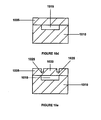
- a micro machined element 100 includes a support structure 105, a mass 110, a resilient coupling 115, and one or more temporary bridges 120.
- the support structure 105 is coupled to the resilient coupling 115. and the temporary bridges 120.
- the support structure 105 is adapted to support the resilient coupling 115 and the temporary bridges 120.
- the mass 110 is coupled to the resilient coupling 115 and the temporary bridges 120.
- the resilient coupling 115 is coupled to the support structure 105 and the mass 110.
- the resilient coupling 115 is adapted to resiliently support the mass 110.
- the mass 110 and resilient coupling 115 are further adapted in a conventional manner to provide a spring-mass system for use in a conventional accelerometer.
- the temporary bridges 120 are coupled to the support structure 105 and the mass 110.
- the temporary bridges 120 are adapted to temporarily support the mass 110 until the temporary bridges 120 are severed during the manufacturing process. In this manner, the temporary bridges 120 prevent damage to the resilient coupling 115 during the manufacturing process.
- the thickness of the temporary bridge 120 is less than the thicknesses of the support structure 105 and the mass 110.
- the thickness of the temporary bridge 120 can be about 1 to 10% of the thickness of the thicknesses of the support structure 105 and the mass 110.
- the thickness of the temporary bridge 120 can be less than about 50 micrometres. In this manner, the structural support of the temporary bridge 120 is maximized while the force required to sever the temporary bridge 120 in minimized.
- the temporary bridge 120 includes one or more cavities 125 in order to further minimize the force required to sever the temporary bridge 120.
- the temporary bridge 120 includes a tapered portion 130 having reduced width in order to further minimize the force required to sever the temporary bridge 120.
- the temporary bridge 120 includes a region 135 of reduced width in order to further minimize the force required to sever the temporary bridge 120.
- the micro machined element 100 can be fabricated from a silicon wafer using one or more of the merged-mask micro machining processes disclosed in U.S. utility patent application serial number 09/352,025, filed on July 13, 1999 .
- a micro machined element 200 includes a support structure 205, a mass 210, resilient couplings 215a and 215b and one or more temporary bridges 220.
- the support structure 205 is coupled to the resilient coupling 215a and 215b and the temporary bridges 120.
- the support structure 205 can be adapted to support the resilient couplings 215a and 215b and the temporary bridges 220.
- the mass 210 is coupled to the resilient couplings 215a and 215b and the temporary bridges 220.
- the resilient couplings 215a and 215b are coupled to the support structure 205 and the mass 210.
- the resilient couplings 215a and 215b can be adapted to resiliently support the mass 210.
- the resilient couplings 215a and 215b can be T-shaped resilient hinges.
- the mass 210 and resilient couplings 215a and 215b can be further adapted to provide a rotating mirror for use in a bar code scanning system as disclosed in U.S. utility patent application serial number 09/352,025 ,
- the temporary bridges 220 are coupled to the support structure 205 and the mass 210.
- the temporary bridges 220 are adapted to temporarily support the mass 210 until the temporary bridges 220 are severed during the manufacturing process. In this manner, the temporary bridges 220 prevent damage to the resilient couplings 215a and 215b during the manufacturing process. Upon the conclusion of the manufacturing process, the temporary bridges 220 are severed and the mass 210 is supported solely by the resilient couplings 215a and 215b.
- the thickness of the temporary bridge 220 is less than the thickness of the support structure 205 and the mass 210.
- the thickness of the temporary bridge 220 can be about 1 to 10% of the thickness of the thicknesses of the support structure 205 and the mass 210.
- the thickness of the temporary bridge 220 can be less than about 50 micrometres. In this manner, the structural support of the temporary bridge 220 is maximized while the force required to sever the temporary bridge 220 is minimized.
- the temporary bridge 220 is tapered in order to further minimize the force required to sever the temporary bridge 220.
- the micro machined element 200 can be fabricated from a silicon wafer using one or more of the merged-mask micro machining processes disclosed in U.S. utility patent application serial number 09/352,025 , filed on july 13, 1999.
- the micro machined element 200 can be coupled to a top cap and a bottom cap, as described in U.S. utility patent application serial number 09/352,025, filed on July 13, 1999 . prior to severing the temporary bridge 220. In this manner, the mass 210 is optimally protected from shock and damage during the subsequent steps of the manufacturing process.
- a method 300 for manufacturing a micro machined structure having one or more temporary bridges includes the steps of: (1) providing a top silicon wafer with an internal layer of silicon dioxide and a bottom silicon wafer in step 305; (2) etching one or more cavities in the top surface of the bottom silicon wafer in step 310; (3) bonding the top surface of the top silicon wafer onto the bottom silicon wafer in step 315; (4) etching the top surface of the top silicon wafer in step 320; and (5) micro machining the top surface of the top silicon wafer to form a three dimensional structure including one or more temporary bridges in step 325.
- a top wafer 405 of silicon having an internal layer 410 of silicon dioxide and a bottom wafer 415 of silicon are provided.
- the top wafer 405 of silicon is a silicon on insulator (SOI) wafer.
- SOI silicon on insulator
- the internal layer 410 of silicon dioxide is positioned about 5 to 50 micrometres above the bottom surface of the top wafer 405 of silicon.
- a cavity 420 is etched in the top surface of the bottom wafer 415 of silicon.
- the cavity 420 may have any number of cross-sectional shapes.
- the cavity 420 can have a substantially rectangular cross-sectional shape.
- the top wafer 405 of silicon is bonded onto the bottom wafer 415 of silicon.
- the top wafer 405 may be bonded to the bottom wafer 415 of silicon using any number of conventional processes for bonding wafers of silicon.
- the top wafer 405 of silicon can be bonded to the bottom wafer 415 of silicon using the process of silicon fusion bonding.
- step 320 the exposed portions of the top wafer 405 and the internal layer 410 of silicon dioxide are etched.
- the exposed portions of the top wafer 405 and the internal layer 410 of silicon dioxide can be etched using a conventional KOH etching process.
- the internal layer 410 of silicon dioxide can be used as an etch stop during the etching process.
- the thickness of the top wafer 405 after the etching process can range from about 5 to 50 micrometres.
- a three dimensional structure 425 is micro machined in the top wafer 405 of silicon above the cavity 420 in the bottom wafer 415 of silicon.
- the structure 425 is coupled to the remaining portions of the top wafer 405 of silicon by one or more temporary bridges 430.
- the structure 425 can be a strain gauge 435.
- the structure 425 and the temporary bridges 430 can be formed using one or more of the merged-mask micro machining processes disclosed in U.S. utility patent serial number 09/352,025, filed on July 13, 1999 .
- the structure 425 is coupled to remaining portions of the top wafer 405 of silicon by temporary bridges 430.
- the structure 425 is then decoupled from the top wafer 405 of silicon by severing the temporary bridges 430. In this manner, the structure is protected from damage prior to subsequent manufacturing operations.
- the temporary bridges 430 can be severed by removing the structure 425 from the top wafer 405 of silicon using a conventional robotic arm.
- the structure 425 can be strain gauge 435 that is decoupled from the top wafer 405 of silicon and subsequently bonded to a substrate and wire bonded.
- a method 500 for manufacturing a micro machined structure having one or more temporary bridges includes the steps of: (1) providing a top silicon wafer with an internal layer of silicon dioxide and a bottom silicon wafer in step 505; (2) etching one or more cavities in the bottom surface of the top silicon wafer in step 510; (3) bonding the top silicon wafer onto the bottom silicon wafer in step 515; (4) etching the top surface of the top silicon wafer in step 520; and (5) micro machining the top surface of the top silicon wafer to form a three dimensional structure including one or more temporary bridges in step 525.
- a top wafer 605 of silicon having an internal layer 610 of silicon dioxide and a bottom wafer 615 of silicon are provided.
- the top wafer 605 of silicon can be an SOI wafer.
- the internal layer 610 of silicon dioxide can be positioned about 5 to 50 micrometres above the bottom surface of the top wafer 605 of silicon.
- a cavity 620 can be etched in the bottom surface of the top wafer 605 of silicon.
- the cavity 620 may have any number of cross-sectional shapes.
- the cavity 620 can have substantially rectangular cross-sectional shape.
- the top wafer 605 of silicon is bonded onto the bottom wafer 615 of silicon.
- the top wafer 605 of silicon may be bonded to the bottom wafer 615 of silicon using any number of conventional processes for bonding wafers of silicon.
- the top wafer 605 of silicon can be bonded to the bottom wafer 615 of silicon using the process of silicon fusion bonding.
- step 520 the exposed portions of the top wafer 605 and the internal layer 610 of silicon dioxide are etched.
- the exposed portions of the top wafer 605 and the internal layer 610 of silicon dioxide are etched using a conventional KOH etching process.
- the internal layer 610 of silicon dioxide is used as an etch stop during the etching process.
- the thickness of the portion of the top wafer 605 of silicon above the cavity 620 after the completion of the etching process can range from about 5 to 50 micrometres.
- a three dimensional structure 625 is micro machined in the top wafer 605 of silicon above the cavity 620 in the bottom surface of the top wafer 605 of silicon.
- the structure 625 is coupled to the remaining portions of the top wafer 605 of silicon by one or more temporary bridges 630.
- the structure 625 and the temporary bridges 630 can be formed using one or more of the merged-mask micro machining processes disclosed in U.S. utility patent application serial number 09/352,025, filed July 13, 1999 .
- the structure 625 is coupled to remaining portions of the top wafer 605 of silicon by the temporary bridge 630.
- the structure 625 is then decoupled from the top wafer 605 of silicon by severing the temporary bridges 630. In this manner, the structure 625 is protected from damage prior to subsequent manufacturing operations.
- the structure 625 can be a strain gauge that is decoupled from the top wafer 605 of silicon and subsequently bonded to a substrate and wire bonded.
- a method 700 for manufacturing a micro machined structure having one or more temporary bridges includes the steps of: (1) providing a top silicon wafer and a bottom silicon wafer in step 705; (2) etching one or more cavities in the bottom surface of the top silicon wafer in step 710; (3) bonding the top silicon wafer onto the bottom silicon wafer in step 715; (4) etching the top surface of the top silicon wafer in step 720; and (5) micro machining the top surface of the top silicon wafer to form a three dimensional structure including one or more temporary bridges in step 725.
- a top wafer 805 of silicon and a bottom wafer 810 of silicon are provided.
- a cavity 815 is etched in the bottom surface of the top wafer 805 of silicon.
- the cavity 815 may have any number of cross-sectional shapes.
- the cavity 815 can have substantially rectangular cross-sectional shape.
- the top wafer 805 of silicon is bonded onto the bottom wafer 810 of silicon.
- the top wafer 805 of silicon may be bonded to the bottom wafer 810 of silicon using any number of conventional processes for bonding wafers of silicon.
- the top wafer 805 of silicon can be bonded to the bottom wafer 810 of silicon using the process of silicon fusion bonding.
- the exposed portions of the top wafer 805 are etched.
- the exposed portions of the top wafer 805 of silicon can be etched using a conventional wet etching process, dry etching process or a wafer polishing process.
- the thickness of the top wafer 805 of silicon above the cavity 815 after the completion of the etching process can range from about 5 to 50 micrometres.
- a three dimensional structure 820 is micro machined in the top wafer 805 of silicon above the cavity 815 in the bottom surface of the top wafer 805 of silicon.
- the structure 820 is coupled to the remaining portions of the top wafer 805 of silicon by one or more temporary bridges 825.
- the structure 820 and the temporary bridges 825 can be formed using one or more of the merged-mask micro machining processes disclosed in U.S. utility patent application serial number 09/352,025, filed on July 13,1999 .
- the structure 820 is coupled to the remaining portions of the top wafer 805 of silicon by the temporary bridges 825.
- the structure 820 is then decoupled from the top wafer 805 of silicon by severing the temporary bridges 825. In this manner, the structure 820 is protected from damage prior to subsequent manufacturing operations.
- the structure 820 can be a strain gauge that is decoupled from the top wafer 805 of silicon and subsequently bonded to a substrate and wire bonded.
- a method 900 of manufacturing a micro machined structure having one or more temporary bridges includes the steps of: (1) providing a top silicon wafer and a bottom silicon wafer in step 905; (2) etching one or more cavities in the top surface of the bottom silicon wafer in step 910; (3) bonding the top silicon wafer onto the bottom silicon wafer in step 915; (4) etching the top surface of the top silicon in step 920; and (5) micro machining the top surface of the top silicon wafer to form a three dimensional structure including one or more temporary bridges in step 925.
- a top wafer 1005 of silicon and a bottom wafer 1010 of silicon are provided.
- a cavity 1015 is etched in the top surface of the bottom wafer 1005 of silicon.
- the cavity 1015 may have any number of cross-sectional shapes.
- the cavity of 1015 can have a substantially rectangular cross-sectional shape.
- the top wafer 1005 of silicon is bonded onto the bottom wafer 1010 of silicon.
- the top wafer 1005 of silicon may be bonded onto the bottom wafer 1010 of silicon using any number of conventional processes for bonding wafers of silicon.
- the top wafer 1005 of silicon can be bonded to the bottom wafer 1010 of silicon using the process of silicon fusion bonding.
- the exposed portions of the top wafer 1005 are etched.
- the exposed portions of the top wafer 1005 of silicon can be etched using a conventional wet etching process, dry etching process, or a wafer polishing process.
- the thickness of the top wafer 1005 of silicon above the cavity 1015 after the completion of the etching process can range from about 5 to 50 micrometres.
- a three dimensional structure 1020 is micro machined in the top wafer 1005 of silicon above the cavity 1015 in the bottom surface of the top wafer 1005 of silicon.
- the structure 1020 is coupled to the remaining portions of the top wafer 1005 of silicon by one or more temporary bridges 1025.
- the structure 1020 and the temporary bridges 1025 can be formed using one or more of the merged-mask micro machining processes disclosed in U.S. utility patent application serial number 09/352,025, filed July 13, 1999 .
- the structure 1020 is coupled to the remaining portions of the top wafer 1005 of silicon by the temporary bridges 1025.
- the structure 1020 is then decoupled from the top wafer 1005 of silicon by severing the temporary bridges 1025. In this manner, the structure 1020 is protected from damage prior to subsequent manufacturing operations.
- the structure 1020 can be a strain gauge that is decoupled from the top wafer 1005 and subsequently bonded to a substrate and wire bonded.
- a micro machined apparatus has been described that includes a support structure, one or more temporary bridges coupled to the support structure, and a mass coupled to the temporary bridge.
- the thickness of the temporary bridges are less than the thicknesses of the support structure and the mass.
- the thickness of the temporary bridges can be about 1 to 10% of the thickness of the support structure and the mass.
- the thickness of the temporary bridges can range from about 5 to 50 micrometres.
- the temporary bridges can include one or more cavities.
- the apparatus further can include one or more resilient couplings coupled to the support and the mass.
- the resilient couplings can be T-shaped hinges.
- the support structure, resilient couplings, and mass can be an accelerometer.
- the support structure, resilient couplings, and mass can be a mirror assembly.
- the mass can be a strain gauge.
- a method of manufacturing a micro machined apparatus also has been described that includes micro machining a support structure coupled to a mass using one or more temporary bridges in a substrate and severing the temporary bridges.
- the mass can be a strain gauge.
- the method further includes micro machining one or more resilient couplings in the substrate for coupling the mass to the support structure.
- the resilient couplings can be T-shaped hinges.
- a method of fabricating a micro machined structure also has been described that includes providing a top silicon wafer and a bottom silicon wafer, forming a cavity in the bottom surface of the top silicon wafer, bonding the top silicon wafer onto the bottom silicon wafer, etching a portion of the top surface of the top silicon wafer and micro machining a three dimensional structure in the portion of the top silicon wafer above the cavity having one or more temporary bridges for coupling the three dimensional structure to the remaining portions of the top silicon wafer.
- the method further includes severing the temporary bridges.
- the three dimensional structure can comprise a strain gauge.
- a method of fabricating a micro machined structure includes providing a top silicon wafer and a bottom silicon wafer, forming a cavity in the top surface of the bottom silicon wafer, bonding the top silicon wafer on to the bottom silicon wafer, etching a portion of the top surface of the top silicon wafer and micro machining a three dimensional structure in the portion of the top silicon wafer above the cavity having one or more temporary bridges for coupling the three dimensional structure to the remaining portions of the top silicon wafer.
- the method further includes severing the temporary bridges.
- the three dimensional structure can comprise a strain gauge.
- a method of fabricating a micro machined structure also has been described that includes providing as top silicon wafer having an internal layer of silicon dioxide and a bottom silicon wafer, forming a cavity in the bottom surface of the top silicon wafer, bonding the top silicon wafer, bonding the top silicon wafer onto the bottom silicon wafer, etching a portion of the top surface of the top surface of the top silicon wafer and micro machining a three dimensional structure in the portion of the top silicon wafer above the cavity having one or more temporary bridges for coupling the three dimensional structure to the remaining portions of the top silicon wafer.
- the method further includes severing the temporary bridges.
- the three dimensional structure can be a strain gauge.
- a method of fabricating a micro machined structure also has been described that includes providing a top silicon wafer having an internal layer of silicon dioxide and a bottom silicon wafer, forming a cavity in the top surface of the bottom silicon wafer, bonding the top silicon wafer onto the bottom silicon wafer, etching a portion of the top surface of the top silicon wafer and micro machining a three dimensional structure in the portion of the top silicon wafer above the cavity having one or more temporary bridges for coupling the three dimensional structure to the remaining portions of the top silicon wafer.
- the method further includes severing the temporary bridges.
- the three dimensional structure can be a strain gauge.
- a method of manufacturing a device including a micro machined structure also has been described that includes temporarily coupling the micro machined structure to a support structure using one or more temporary bridges, decoupling the micro machined structure form the support structure by severing the temporary bridges and coupling the micro machined structure to a substrate.
- a method of protecting a resilient coupling for coupling a mass to a support structure also has been described that includes coupling the mass to the support structure using the resilient coupling and one or more temporary bridges and severing the temporary bridges.
Landscapes
- Engineering & Computer Science (AREA)
- Manufacturing & Machinery (AREA)
- Microelectronics & Electronic Packaging (AREA)
- Physics & Mathematics (AREA)
- General Physics & Mathematics (AREA)
- Optics & Photonics (AREA)
- Micromachines (AREA)
- Pressure Sensors (AREA)
- Bridges Or Land Bridges (AREA)
- Golf Clubs (AREA)
- Electrophonic Musical Instruments (AREA)
- Slide Fasteners, Snap Fasteners, And Hook Fasteners (AREA)
- Particle Formation And Scattering Control In Inkjet Printers (AREA)
- Organic Low-Molecular-Weight Compounds And Preparation Thereof (AREA)
Applications Claiming Priority (3)
| Application Number | Priority Date | Filing Date | Title |
|---|---|---|---|
| US09/406,158 US6458513B1 (en) | 1999-07-13 | 1999-09-27 | Temporary bridge for micro machined structures |
| US406158 | 1999-09-27 | ||
| PCT/US2000/026355 WO2001024228A2 (en) | 1999-09-27 | 2000-09-25 | Temporary bridge for micro machined structures |
Publications (3)
| Publication Number | Publication Date |
|---|---|
| EP1252028A2 EP1252028A2 (en) | 2002-10-30 |
| EP1252028A4 EP1252028A4 (en) | 2006-03-01 |
| EP1252028B1 true EP1252028B1 (en) | 2009-08-12 |
Family
ID=23606774
Family Applications (1)
| Application Number | Title | Priority Date | Filing Date |
|---|---|---|---|
| EP00966870A Expired - Lifetime EP1252028B1 (en) | 1999-09-27 | 2000-09-25 | Method of fabricating a micro machined structure |
Country Status (9)
| Country | Link |
|---|---|
| US (1) | US6458513B1 (enExample) |
| EP (1) | EP1252028B1 (enExample) |
| JP (1) | JP2003510194A (enExample) |
| AT (1) | ATE439249T1 (enExample) |
| AU (1) | AU7715200A (enExample) |
| CA (1) | CA2384889C (enExample) |
| DE (1) | DE60042757D1 (enExample) |
| NO (1) | NO20021507D0 (enExample) |
| WO (1) | WO2001024228A2 (enExample) |
Families Citing this family (8)
| Publication number | Priority date | Publication date | Assignee | Title |
|---|---|---|---|---|
| US6693245B2 (en) * | 2000-09-29 | 2004-02-17 | Anritsu Corporation | Electronic balance which is easily assembled, maintained, downsized and improved with respect to weighing performance, and method for manufacturing the same |
| US6818464B2 (en) * | 2001-10-17 | 2004-11-16 | Hymite A/S | Double-sided etching technique for providing a semiconductor structure with through-holes, and a feed-through metalization process for sealing the through-holes |
| WO2003098302A2 (en) * | 2002-05-15 | 2003-11-27 | Hymite A/S | Optical device receiving substrate and optical device holding carrier |
| US7681306B2 (en) | 2004-04-28 | 2010-03-23 | Hymite A/S | Method of forming an assembly to house one or more micro components |
| JP4651476B2 (ja) * | 2005-07-29 | 2011-03-16 | 株式会社リコー | 光走査装置の組立方法および光走査装置ならびに画像形成装置 |
| EP1967317A1 (en) * | 2007-03-07 | 2008-09-10 | Fujitsu Limited | Method for separating a workpiece and laser processing apparatus |
| CN103149684B (zh) * | 2013-02-07 | 2015-01-28 | 东南大学 | 可双向扭转的交错梳齿静电驱动可变光衰减器及制备方法 |
| WO2021194316A1 (ko) * | 2020-03-26 | 2021-09-30 | 주식회사 위멤스 | 광스캐너 패키지 및 제조 방법 |
Family Cites Families (18)
| Publication number | Priority date | Publication date | Assignee | Title |
|---|---|---|---|---|
| JPS62190748A (ja) * | 1986-02-17 | 1987-08-20 | Nissan Motor Co Ltd | 半導体加速度センサ組立方法 |
| US5060039A (en) * | 1988-01-13 | 1991-10-22 | The Charles Stark Draper Laboratory, Inc. | Permanent magnet force rebalance micro accelerometer |
| US5534111A (en) * | 1988-02-29 | 1996-07-09 | Honeywell Inc. | Thermal isolation microstructure |
| JPH04258175A (ja) * | 1991-02-12 | 1992-09-14 | Mitsubishi Electric Corp | シリコン半導体加速度センサの製造方法 |
| JP3293194B2 (ja) * | 1992-10-13 | 2002-06-17 | 株式会社デンソー | 力学量センサ |
| JPH06350105A (ja) * | 1993-06-07 | 1994-12-22 | Nec Corp | マイクロマシンとその製造方法 |
| US5364497A (en) | 1993-08-04 | 1994-11-15 | Analog Devices, Inc. | Method for fabricating microstructures using temporary bridges |
| JP2775578B2 (ja) * | 1993-09-20 | 1998-07-16 | 仗祐 中田 | 加速度センサとその製造方法 |
| US5369057A (en) * | 1993-12-21 | 1994-11-29 | Delco Electronics Corporation | Method of making and sealing a semiconductor device having an air path therethrough |
| JPH07240395A (ja) * | 1994-02-28 | 1995-09-12 | Matsushita Electric Works Ltd | 半導体装置の製造方法 |
| US5481102A (en) * | 1994-03-31 | 1996-01-02 | Hazelrigg, Jr.; George A. | Micromechanical/microelectromechanical identification devices and methods of fabrication and encoding thereof |
| JPH1096744A (ja) * | 1996-09-20 | 1998-04-14 | Zexel Corp | 容量型加速度センサの製造方法 |
| JPH10163505A (ja) * | 1996-11-29 | 1998-06-19 | Mitsubishi Materials Corp | 半導体慣性センサ及びその製造方法 |
| JPH1172505A (ja) * | 1997-06-17 | 1999-03-16 | Denso Corp | 加速度センサおよびその製造方法 |
| JPH1140820A (ja) * | 1997-07-18 | 1999-02-12 | Denso Corp | 半導体力学量センサの製造方法 |
| US6321134B1 (en) * | 1997-07-29 | 2001-11-20 | Silicon Genesis Corporation | Clustertool system software using plasma immersion ion implantation |
| EP1031736B1 (en) * | 1999-02-26 | 2004-04-28 | STMicroelectronics S.r.l. | Process for manufacturing mechanical, electromechanical and opto-electromechanical microstructures having suspended regions subject to mechanical stresses during assembly |
| JP3580179B2 (ja) * | 1999-05-26 | 2004-10-20 | 松下電工株式会社 | 半導体加速度センサの製造方法 |
-
1999
- 1999-09-27 US US09/406,158 patent/US6458513B1/en not_active Expired - Lifetime
-
2000
- 2000-09-25 DE DE60042757T patent/DE60042757D1/de not_active Expired - Lifetime
- 2000-09-25 AU AU77152/00A patent/AU7715200A/en not_active Abandoned
- 2000-09-25 WO PCT/US2000/026355 patent/WO2001024228A2/en not_active Ceased
- 2000-09-25 AT AT00966870T patent/ATE439249T1/de not_active IP Right Cessation
- 2000-09-25 EP EP00966870A patent/EP1252028B1/en not_active Expired - Lifetime
- 2000-09-25 CA CA2384889A patent/CA2384889C/en not_active Expired - Lifetime
- 2000-09-25 JP JP2001527321A patent/JP2003510194A/ja active Pending
-
2002
- 2002-03-26 NO NO20021507A patent/NO20021507D0/no not_active Application Discontinuation
Also Published As
| Publication number | Publication date |
|---|---|
| EP1252028A4 (en) | 2006-03-01 |
| CA2384889A1 (en) | 2001-04-05 |
| AU7715200A (en) | 2001-04-30 |
| NO20021507L (no) | 2002-03-26 |
| DE60042757D1 (de) | 2009-09-24 |
| WO2001024228A3 (en) | 2002-03-14 |
| US6458513B1 (en) | 2002-10-01 |
| WO2001024228A2 (en) | 2001-04-05 |
| CA2384889C (en) | 2010-05-04 |
| ATE439249T1 (de) | 2009-08-15 |
| NO20021507D0 (no) | 2002-03-26 |
| EP1252028A2 (en) | 2002-10-30 |
| JP2003510194A (ja) | 2003-03-18 |
Similar Documents
| Publication | Publication Date | Title |
|---|---|---|
| US7083997B2 (en) | Bonded wafer optical MEMS process | |
| US5130276A (en) | Method of fabricating surface micromachined structures | |
| EP2259301B1 (en) | Method for preparing and assembling substrates | |
| US7767484B2 (en) | Method for sealing and backside releasing of microelectromechanical systems | |
| ATE511493T1 (de) | Verfahren zur herstellung von genauen mikroelektromechanischen strukturen, und so hergestellte mikrostrukturen | |
| US7399652B2 (en) | Method for manufacturing a micro-electro-mechanical device, in particular an optical microswitch, and micro-electro-mechanical device thus obtained | |
| AU5874099A (en) | Formation of suspended beams using soi substrates, and application to the fabrication of a vibratory gyrometer | |
| EP0763255A1 (en) | Substrate anchor for undercut silicon on insulator microstructures | |
| EP3249371B1 (en) | Differential pressure sensor full overpressure protection device | |
| US20030077881A1 (en) | Method for manipulating MEMS devices, integrated on a wafer semiconductor and intended to be diced one from the other, and relevant support | |
| EP1252028B1 (en) | Method of fabricating a micro machined structure | |
| EP2019081A2 (en) | Boron doped shell for MEMS device | |
| US7387737B2 (en) | Method for fabricating an isolated microelectromechanical system (MEMS) device using an internal void | |
| US8614110B1 (en) | Method for fabricating a dual-crystalline silicon suspension system using pre-fabricated cavities | |
| EP1375416B1 (en) | Micro-electro-mechanical device, in particular micro-actuator for hard-disk drive, and manufacturing process thereof | |
| US7514286B2 (en) | Method for forming individual semi-conductor devices | |
| US6544898B2 (en) | Method for improved die release of a semiconductor device from a wafer | |
| JP2000155030A (ja) | 角速度センサの製造方法 | |
| EP1333008B1 (en) | Systems and methods for thermal isolation of a silicon structure | |
| US20030119275A1 (en) | Process for manufacturing a two-axis mirror | |
| EP1031736B1 (en) | Process for manufacturing mechanical, electromechanical and opto-electromechanical microstructures having suspended regions subject to mechanical stresses during assembly | |
| JP2007015101A (ja) | 隠れヒンジmemsデバイス | |
| KR100324716B1 (ko) | 미세구조물 패키징방법 | |
| RU2830141C1 (ru) | Способ соединения кремниевых пластин | |
| US7256128B2 (en) | Method of double-sided etching |
Legal Events
| Date | Code | Title | Description |
|---|---|---|---|
| PUAI | Public reference made under article 153(3) epc to a published international application that has entered the european phase |
Free format text: ORIGINAL CODE: 0009012 |
|
| 17P | Request for examination filed |
Effective date: 20020429 |
|
| AK | Designated contracting states |
Kind code of ref document: A2 Designated state(s): AT BE CH CY DE DK ES FI FR GB GR IE IT LI LU MC NL PT SE |
|
| AX | Request for extension of the european patent |
Free format text: AL;LT;LV;MK;RO;SI |
|
| RAP1 | Party data changed (applicant data changed or rights of an application transferred) |
Owner name: INPUT/OUTPUT, INC. |
|
| RBV | Designated contracting states (corrected) |
Designated state(s): AT BE CH CY DE DK FR GB LI NL |
|
| A4 | Supplementary search report drawn up and despatched |
Effective date: 20060118 |
|
| RAP1 | Party data changed (applicant data changed or rights of an application transferred) |
Owner name: INPUT/OUTPUT, INC. |
|
| RAP1 | Party data changed (applicant data changed or rights of an application transferred) |
Owner name: ION GEOPHYSICAL CORPORATION |
|
| RTI1 | Title (correction) |
Free format text: METHOD OF FABRICATING A MICRO MACHINED STRUCTURE |
|
| GRAP | Despatch of communication of intention to grant a patent |
Free format text: ORIGINAL CODE: EPIDOSNIGR1 |
|
| GRAS | Grant fee paid |
Free format text: ORIGINAL CODE: EPIDOSNIGR3 |
|
| GRAA | (expected) grant |
Free format text: ORIGINAL CODE: 0009210 |
|
| AK | Designated contracting states |
Kind code of ref document: B1 Designated state(s): AT CH DE FR GB LI NL |
|
| REG | Reference to a national code |
Ref country code: GB Ref legal event code: FG4D |
|
| REG | Reference to a national code |
Ref country code: CH Ref legal event code: EP |
|
| REF | Corresponds to: |
Ref document number: 60042757 Country of ref document: DE Date of ref document: 20090924 Kind code of ref document: P |
|
| PG25 | Lapsed in a contracting state [announced via postgrant information from national office to epo] |
Ref country code: AT Free format text: LAPSE BECAUSE OF FAILURE TO SUBMIT A TRANSLATION OF THE DESCRIPTION OR TO PAY THE FEE WITHIN THE PRESCRIBED TIME-LIMIT Effective date: 20090812 |
|
| REG | Reference to a national code |
Ref country code: CH Ref legal event code: PL |
|
| PLBE | No opposition filed within time limit |
Free format text: ORIGINAL CODE: 0009261 |
|
| STAA | Information on the status of an ep patent application or granted ep patent |
Free format text: STATUS: NO OPPOSITION FILED WITHIN TIME LIMIT |
|
| 26N | No opposition filed |
Effective date: 20100517 |
|
| PG25 | Lapsed in a contracting state [announced via postgrant information from national office to epo] |
Ref country code: LI Free format text: LAPSE BECAUSE OF NON-PAYMENT OF DUE FEES Effective date: 20090930 Ref country code: CH Free format text: LAPSE BECAUSE OF NON-PAYMENT OF DUE FEES Effective date: 20090930 |
|
| PGFP | Annual fee paid to national office [announced via postgrant information from national office to epo] |
Ref country code: DE Payment date: 20110329 Year of fee payment: 11 |
|
| REG | Reference to a national code |
Ref country code: DE Ref legal event code: R119 Ref document number: 60042757 Country of ref document: DE Effective date: 20130403 |
|
| PG25 | Lapsed in a contracting state [announced via postgrant information from national office to epo] |
Ref country code: DE Free format text: LAPSE BECAUSE OF NON-PAYMENT OF DUE FEES Effective date: 20130403 |
|
| REG | Reference to a national code |
Ref country code: FR Ref legal event code: PLFP Year of fee payment: 17 |
|
| REG | Reference to a national code |
Ref country code: FR Ref legal event code: PLFP Year of fee payment: 18 |
|
| REG | Reference to a national code |
Ref country code: FR Ref legal event code: PLFP Year of fee payment: 19 |
|
| PGFP | Annual fee paid to national office [announced via postgrant information from national office to epo] |
Ref country code: NL Payment date: 20180912 Year of fee payment: 19 Ref country code: GB Payment date: 20180919 Year of fee payment: 19 |
|
| PGFP | Annual fee paid to national office [announced via postgrant information from national office to epo] |
Ref country code: FR Payment date: 20190815 Year of fee payment: 20 |
|
| REG | Reference to a national code |
Ref country code: NL Ref legal event code: MM Effective date: 20191001 |
|
| PG25 | Lapsed in a contracting state [announced via postgrant information from national office to epo] |
Ref country code: NL Free format text: LAPSE BECAUSE OF NON-PAYMENT OF DUE FEES Effective date: 20191001 |
|
| GBPC | Gb: european patent ceased through non-payment of renewal fee |
Effective date: 20190925 |
|
| PG25 | Lapsed in a contracting state [announced via postgrant information from national office to epo] |
Ref country code: GB Free format text: LAPSE BECAUSE OF NON-PAYMENT OF DUE FEES Effective date: 20190925 |