EP1249865A2 - Vielschichtige metallische dünne Barriereschichten für Kupfer-Zwischenverbindungen, abgeschieden durch ALCVD - Google Patents
Vielschichtige metallische dünne Barriereschichten für Kupfer-Zwischenverbindungen, abgeschieden durch ALCVD Download PDFInfo
- Publication number
- EP1249865A2 EP1249865A2 EP02006940A EP02006940A EP1249865A2 EP 1249865 A2 EP1249865 A2 EP 1249865A2 EP 02006940 A EP02006940 A EP 02006940A EP 02006940 A EP02006940 A EP 02006940A EP 1249865 A2 EP1249865 A2 EP 1249865A2
- Authority
- EP
- European Patent Office
- Prior art keywords
- barrier metal
- thin film
- metal thin
- chemical species
- film
- Prior art date
- Legal status (The legal status is an assumption and is not a legal conclusion. Google has not performed a legal analysis and makes no representation as to the accuracy of the status listed.)
- Withdrawn
Links
Images


Classifications
-
- H—ELECTRICITY
- H10—SEMICONDUCTOR DEVICES; ELECTRIC SOLID-STATE DEVICES NOT OTHERWISE PROVIDED FOR
- H10W—GENERIC PACKAGES, INTERCONNECTIONS, CONNECTORS OR OTHER CONSTRUCTIONAL DETAILS OF DEVICES COVERED BY CLASS H10
- H10W20/00—Interconnections in chips, wafers or substrates
- H10W20/01—Manufacture or treatment
- H10W20/031—Manufacture or treatment of conductive parts of the interconnections
- H10W20/032—Manufacture or treatment of conductive parts of the interconnections of conductive barrier, adhesion or liner layers
- H10W20/033—Manufacture or treatment of conductive parts of the interconnections of conductive barrier, adhesion or liner layers in openings in dielectrics
- H10W20/035—Manufacture or treatment of conductive parts of the interconnections of conductive barrier, adhesion or liner layers in openings in dielectrics combinations of barrier, adhesion or liner layers, e.g. multi-layered barrier layers
-
- H—ELECTRICITY
- H10—SEMICONDUCTOR DEVICES; ELECTRIC SOLID-STATE DEVICES NOT OTHERWISE PROVIDED FOR
- H10P—GENERIC PROCESSES OR APPARATUS FOR THE MANUFACTURE OR TREATMENT OF DEVICES COVERED BY CLASS H10
- H10P14/00—Formation of materials, e.g. in the shape of layers or pillars
- H10P14/40—Formation of materials, e.g. in the shape of layers or pillars of conductive or resistive materials
- H10P14/42—Formation of materials, e.g. in the shape of layers or pillars of conductive or resistive materials using a gas or vapour
- H10P14/43—Chemical deposition, e.g. chemical vapour deposition [CVD]
- H10P14/432—Chemical deposition, e.g. chemical vapour deposition [CVD] using selective deposition
-
- H—ELECTRICITY
- H10—SEMICONDUCTOR DEVICES; ELECTRIC SOLID-STATE DEVICES NOT OTHERWISE PROVIDED FOR
- H10W—GENERIC PACKAGES, INTERCONNECTIONS, CONNECTORS OR OTHER CONSTRUCTIONAL DETAILS OF DEVICES COVERED BY CLASS H10
- H10W20/00—Interconnections in chips, wafers or substrates
- H10W20/01—Manufacture or treatment
- H10W20/031—Manufacture or treatment of conductive parts of the interconnections
- H10W20/032—Manufacture or treatment of conductive parts of the interconnections of conductive barrier, adhesion or liner layers
-
- H—ELECTRICITY
- H10—SEMICONDUCTOR DEVICES; ELECTRIC SOLID-STATE DEVICES NOT OTHERWISE PROVIDED FOR
- H10W—GENERIC PACKAGES, INTERCONNECTIONS, CONNECTORS OR OTHER CONSTRUCTIONAL DETAILS OF DEVICES COVERED BY CLASS H10
- H10W20/00—Interconnections in chips, wafers or substrates
- H10W20/01—Manufacture or treatment
- H10W20/031—Manufacture or treatment of conductive parts of the interconnections
- H10W20/056—Manufacture or treatment of conductive parts of the interconnections by filling conductive material into holes, grooves or trenches
-
- H—ELECTRICITY
- H10—SEMICONDUCTOR DEVICES; ELECTRIC SOLID-STATE DEVICES NOT OTHERWISE PROVIDED FOR
- H10W—GENERIC PACKAGES, INTERCONNECTIONS, CONNECTORS OR OTHER CONSTRUCTIONAL DETAILS OF DEVICES COVERED BY CLASS H10
- H10W20/00—Interconnections in chips, wafers or substrates
- H10W20/01—Manufacture or treatment
- H10W20/031—Manufacture or treatment of conductive parts of the interconnections
- H10W20/032—Manufacture or treatment of conductive parts of the interconnections of conductive barrier, adhesion or liner layers
- H10W20/0375—Manufacture or treatment of conductive parts of the interconnections of conductive barrier, adhesion or liner layers comprising multiple stacked thin barrier, adhesion or liner layers not being formed in openings in dielectrics
Definitions
- This invention relates to a multi-layered barrier metal thin film and a method of producing the same and, more particularly, to a multi-layered barrier metal thin film for copper interconnect wherein the multi-layered structure is manufactured by atomic layer chemical vapor deposition.
- the thickness of the barrier metal thin film for interconnect metallization within the device is also forced to be reduced.
- the properties of the barrier metal thin film such as its anti-diffusion capability, low resistivity, high density, step coverage, and other such properties, are required to remain the same or even improve.
- MOCVD metal organic chemical vapor deposition
- Plasma densification performed on conventional chemical vapor deposition (CVD) barrier metal films may extend the capabilities of conventional CVD technology.
- CVD chemical vapor deposition
- the film properties of the barrier metal film deposited on a side wall of a trench or a via are different from the film properties of the film deposited on the horizontal surfaces of the deposition surface.
- the blocking diffusion capability of the film is therefore reduced on the side wall of the trench or the via.
- conventional CVD barrier films contain carbon and other impurities that affect the density and resistivity of as-deposited barrier metal thin films. Accordingly, current technology is limited with regard to the thickness to which barrier metal films can be reduced and with regard to the properties of barrier metal films.
- a multi-layered barrier metal thin film is deposited on a substrate by atomic layer chemical vapor deposition (ALCVD).
- the multi-layer film may comprise several different layers of a single chemical species, or several layers each of distinct or alternating chemical species.
- the multi-layer barrier thin film comprises a Tantalum Nitride (TaN) layer on a substrate with a Titanium Nitride (TiN) layer deposited thereon.
- TiN Titanium Nitride
- the thickness of the entire multi-layer film is typically as small as fifty Angstroms.
- the film has superior film characteristics, such as anti-diffusion capability, low resistivity, high density, and step coverage, when compared to films deposited by conventional chemical vapor deposition (CVD).
- the multi-layered barrier metal thin film of the present invention has improved adhesion characteristics and is particularly suited for metallization of a Copper film thereon.
- an object of the invention is to provide a multi-layer barrier metal film, and a method of producing the same.
- Another object of the invention is to provide a multi-layer barrier metal film, and a method of producing the same, having improved film characteristics.
- a further object of the invention is to provide a multi-layer barrier metal film, and a method of producing the same, wherein said film comprises multiple layers of a single chemical species, or several layers of distinct chemical species, deposited by the method of atomic layer chemical vapor deposition.
- Still a further object of the invention is to provide a multi-layer barrier metal film having improved adhesion characteristics for the metallization of a Copper film thereon.
- FIG. 1 is a schematic of the method of atomic layer chemical vapor deposition to deposit a multi-layer barrier metal film on a substrate.
- FIG. 2 is a schematic of the deposited multi-layer barrier metal film of FIG. 1.
- FIG. 3 is a detailed cross sectional view of the first deposited layer of a multi-layer barrier metal film.
- FIG. 4 is a detailed cross sectional view of a multi-layer barrier metal film comprising two layers each of a distinct chemical species.
- FIG. 5 shows the multi-layer barrier metal film of FIG. 4 with a Copper layer deposited thereon.
- FIG. 6 shows a multi-layer barrier metal film having four layers and a Copper layer deposited thereon.
- FIG. 7 is flowchart of the method of the present invention.
- Atomic layer chemical vapor deposition is an emerging technology that is being adopted in mainstream semiconductor research for eventual transfer to manufacturing.
- ALCVD uses fast operating valves to deliver individual reactants to a deposition chamber. Each reactant lays a mono-layer, i.e., an atomic layer, or several mono-layers, on the wafer structure through chemical adsorption and reacts with a previously deposited mono-layer species to form a desired compound.
- the as-formed compound will have a higher density than can be achieved by conventional CVD methods.
- the as-formed compound will also have excellent step coverage. By carefully selecting precursors, multi-layered or alternating layered barrier metal films are achievable.
- Tantalum Nitride/Silicon Nitride TiN/SiN
- Tantalum Nitride/Titanium Nitride TiN/TiN
- Titanium Nitride/Silicon Nitride TiN/SiN thin films, or their combinations, are relatively easy to deposit using the ALCVD technology of the present invention.
- the entire film stack thickness typically is less than 100 Angstroms (100 A), preferably is less than 60 A, and can be as low as fifty Angrstroms (50A), and can exhibit superior barrier film properties.
- a direct application for ALCVD barrier metal films deposited by the current invention is the multi-layered TaN/TiN film stack.
- TaN films have better barrier properties when compared to TiN but often exhibit poor adhesion for the subsequently deposited Copper (Cu) film, when compared to adhesion characteristics of TiN films.
- Single layer films also form grain structures that permit some diffusion along the grain boundaries. Accordingly a single layer film of either TaN or TiN has disadvantages.
- the TaN/TiN multi-layer stack therefore, would be an attractive alternative for a barrier film for Cu metallization.
- ALCVD barrier metal multi-layer thin films controlled to the atomic layer level are not possible with other deposition techniques.
- the ability to alternate from TiN to TaN, or to SiN, over several layers is unique to atomic layer chemical vapor deposition.
- the layer deposition achieved is also insensitive to surface orientation because of its self limited growth character, which means that the multi-layered deposition should be conformal and very uniform.
- a thin layer of the multi-layer structure of the present invention should prevent diffusion of Copper metal as well as a much thicker, more pure Nitride of just Titanium or just Tantalum.
- the film density and resistivity of the thin multi-layer structure should also be superior to the thicker, pure TiN or pure TaN structure.
- FIG. 1 shows a schematic of the atomic layer chemical vapor deposition (ALCVD) process of the present invention.
- a substrate 10 is shown with a first chemical species 12 attached to a surface 14 of the substrate by the process of chemical adsorption.
- substrate is used herein to mean any type of structre adapted for the adsorption of first chemical species 12 thereon.
- substrate 10 may comprise a substrate as defined by conventional standards or may comprise the outermost layer of a previously deposited multi-layer stack, or any other such structure that defines a surface adapted for adsorption of chemical species 12 thereon.
- substrate 10 may comprise a substrate having the following general formulas: SiOx, SiOC, and other polymer materials, typically having a low-k.
- Substrate 10 typically is positioned within a deposition chamber 16 which includes one or more valves, such as valves 18 and 20, and which defines an atmosphere 22 within said chamber. Substrate 10, and more particularly, surface 14 of the substrate, is in contact with atmosphere 22 of chamber 16.
- first chemical species 12 is released into chamber 16 by a valve, such as valve 18.
- Valves 18 and 20 are fast operating valves that are capable of delivering individual reactants, or species, in predetermined quantities. The speed of the valves allows for operation times as short as a fraction of a second, such as approximately 0.4 second reaction times, depending on the chamber size.
- first chemical species 12 attaches to surface 14 of substrate 10 by chemical adsorption.
- First chemical species 12 forms a mono-layer (i.e., one molecule thickness, or one atomic thickness), or several mono-layers (i.e., several molecules thick), 24 on surface 14.
- Chamber 16 is then cleared of the remaining first chemical species 12 within atmosphere 22 that is not adsorbed on surface 14. Purging of the chamber typically takes approximately three or four seconds, depending on the chamber size.
- Valve 20, for example, may then introduce a second chemical species 26 into atmosphere 22.
- Second chemical species 26 reacts with first chemical species 12 in mono-layer 24 in a reaction represented by arrow 28.
- Reaction by-products 30 may or may not be released, depending on the chemical species utilized during reaction 28.
- the first chemical species 12 may comprise a metal halide and the second chemical species 26 may comprise ammonia, an amine, other nitrogen gasses, or the like.
- the deposited film typically is a metal nitride and the by-products typically comprise halide acids, nitrogen, and the like.
- first chemical species 12 may comrpise TiCl 4 and second chemical species 26 may comprise NH 3 .
- the reaction results in a TiN film being deposited on surface 14, and reaction by-products 30 comprise HCl and N 2 .
- the reaction is set forth in Equation (1).
- the wafer temperature typically varies with the chemical species used in making the metal nitride thin film. Typically, the wafer temperature may be/in a range of 300 to 600 °C.
- the pressure of the reaction typically is not an important factor in ALCVD processes. However, the pressure typically will be in a range of 0.001 to 1.0 torr, depending on the reactor size.
- the time period of the reaction typically ranges from 0.4 to five seconds for introducing each species, which may vary by reactor size and chemical species. Several seconds typically is required for purging the reactor vessel between species.
- Equation (2) For the deposition of a TaN mono-layer, the following reaction, shown in Equation (2), may be utilized.
- FIG. 2 shows the results of reaction 28, namely, the formation of a compound 32 secured to surface 14 of substrate 10.
- Compound 32 defines one layer 34 of the multi-layer barrier metal structure, wherein the multi-layered structure has improved film characteristics, such as anti-diffusion capability, low resistivity, high density, and good step coverage, when compared to films deposited by conventional chemical vapor deposition (CVD).
- the multi-layered barrier metal thin film 34 also has improved adhesion characteristics and is particularly suited for metallization of a Copper film thereon.
- Layer 34 may comprise titanium nitride (TiN), tantalum nitride (TaN), tungsten (W), tungsten nitride (WN)or silicon nitride (Si 3 N 4 ).
- the ALCVD process disclosed herein results in an isotropic multi-layer film (shown in FIG. 4) comprised of multiple mono-layers 34 that are evenly distributed across surface 14 and throughout a trench or a via 36 in substrate 10.
- trench 36 is shown, merely for ease of illustration, in a size that is out of proportion with respect to the size of the chemical species.
- Film 34 is evenly distributed on side walls 38 and on the horizontal surfaces, such as bottom surface 40, of trench or via 36 such that the side walls and the bottom surface of the trench have the same or similar film properties. Accordingly, the blocking capability of side walls 38 is not reduced with respect to bottom surface 40 of the trench or via, as is the case with films produced by prior art CVD processes.
- mono-layer barrier metal film 34 does not contain carbon or other impurities that may affect the density and resistivity of the as-deposited multi-layer barrier film or films.
- more that two layers may be deposited on substrate 10.
- five sets of first and second chemical species may be sequentially introduced into chamber 16 for reaction with the previously deposited mono-layer.
- the multiple layers may each be a unique chemical species, the same species, a particular chemical species may be used alternately between different chemical species, or any other combination as is desired.
- the first chemical species attaches to the deposition surface by chemical adsorption and reacts with a previously deposited mono-layer species, or the substrate surface in the case of the first deposited reactant.
- the second chemical species is then added to the reactant chamber to react with the first chemical species to form the mono-layer.
- Subsequent layers repeat the process by laying a mono-layer on the previous deposited layer. In this manner, the film stack is created having the desired film properties.
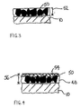
- FIG. 3 shows a detailed cross sectional view of the first deposited layer 50 of the multi-layer barrier metal film.
- First layer 50 in a preferred embodiment, comprises TaN which has superior barrier properties but low adhesion characteristics for the deposition of Copper thereon.
- first layer 50 is controlled to the atomic level, i.e., layer 50 has a thickness 52 which is the thickness of the TaN compound itself. Accordingly, the thickness of layer 50 is much smaller than the thickness of films heretofore achievable from prior art CVD processes. However, in other embodiments, thickness 52 may be on the order of several TaN molecules.
- FIG. 4 shows a detailed cross sectional view of a second deposited layer 54 deposited on first deposited layer 50 of multi-layer barrier metal film 48.
- Layers 50 and 54 together define a thickness 56 of film 48.
- layer 54 comprises TiN so that layers 50 and 54 each comprise a distinct chemical species.
- the TiN layer may not have the same barrier properties of the TaN layer, but the TiN layer typically provides good adhesion for deposition of a copper thin film thereon.
- Thickness 56 of the two layers may be on the order of 50 Angstroms and typically will be less than 100A.
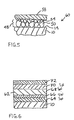
- FIG. 5 shows the multi-layer barrier metal film of FIG. 4 with a Copper layer 58 deposited thereon.
- Upper or outermost layer 54 of stack 48 comprises TiN which has superior adhesion properties for the deposition of a Copper film thereon, when compared to the adhesion properties of a TaN film. Accordingly, Copper layer 58 typically will withstand standard tape tests and will resist peeling or flaking from multi-layer barrier metal film 48.
- Semiconductor device 60 which includes Copper film 58 and multi-layer barrier film 48, therefore, can be manufactured in a small size, and having superior film properties, than heretofore available.
- FIG. 6 shows a schematic of a multi-layer barrier metal film 62 having four layers, 64, 66, 68 and 70, each deposited by ALCVD. Innermost layer 64 is deposited by ALCVD on substrate 10. A Copper film 72 is adhered to the outermost layer 70 of the multi-layer stack 62.
- layers 64 and 68 may comprise TaN whereas layers 66 and 70 may comprise IEN.
- each of layers 64, 66, 68 and 70 may comprise TaN, TiN or Si 3 N 4 so that a multi-layered structure 62 with a variety of layering sequences may be utilized. Of course, other numbers of mono-layers within the stack may be utilized.
- FIG. 7 is a flowchart of the method of the present invention.
- Step 76 comprises providing a substrate having an exposed surface for the ALCVD reaction of a chemical species thereon.
- Step 78 comprises providing chemical species, or reactants, to the exposed surface of the substrate.
- Step 80 comprises reacting the reactants by ALCVD on the exposed surface of the substrate. This step typically takes place in an ALCVD chamber.
- the chamber will have a pressure in a range of 0.001 to 1.0 torr, a temperature in a range of 300 to 600 °C, and a reaction time of approximately one second.
- Step 82 comprises removing the by-products of the reaction of step 80.
- Step 84 comprises deciding whether another layer in the multi-layer stack is desired. If so, the process returns to step 78 for repetition of the reaction with subsequent first and second chemical species. If not, the multi-layer barrier metal layer is complete.
- Step 86 comprises providing Copper to the reactant chamber.
- Step 88 comprises reacting the Copper, or other such subsequent layer or device, on the outermost layer of the multi-layer stack.
- TiN is the outermost layer, which easily allows the adhesion of Copper thereto
- TaN is an inner layer having superior barrier qualitites.
Landscapes
- Chemical Vapour Deposition (AREA)
- Internal Circuitry In Semiconductor Integrated Circuit Devices (AREA)
- Electrodes Of Semiconductors (AREA)
Applications Claiming Priority (2)
| Application Number | Priority Date | Filing Date | Title |
|---|---|---|---|
| US819296 | 1986-01-16 | ||
| US09/819,296 US7015138B2 (en) | 2001-03-27 | 2001-03-27 | Multi-layered barrier metal thin films for Cu interconnect by ALCVD |
Publications (2)
| Publication Number | Publication Date |
|---|---|
| EP1249865A2 true EP1249865A2 (de) | 2002-10-16 |
| EP1249865A3 EP1249865A3 (de) | 2004-01-02 |
Family
ID=25227748
Family Applications (1)
| Application Number | Title | Priority Date | Filing Date |
|---|---|---|---|
| EP02006940A Withdrawn EP1249865A3 (de) | 2001-03-27 | 2002-03-26 | Vielschichtige metallische dünne Barriereschichten für Kupfer-Zwischenverbindungen, abgeschieden durch ALCVD |
Country Status (4)
| Country | Link |
|---|---|
| US (2) | US7015138B2 (de) |
| EP (1) | EP1249865A3 (de) |
| JP (1) | JP2002329680A (de) |
| KR (1) | KR20020076178A (de) |
Families Citing this family (9)
| Publication number | Priority date | Publication date | Assignee | Title |
|---|---|---|---|---|
| US7426067B1 (en) * | 2001-12-17 | 2008-09-16 | Regents Of The University Of Colorado | Atomic layer deposition on micro-mechanical devices |
| US7087480B1 (en) * | 2002-04-18 | 2006-08-08 | Taiwan Semiconductor Manufacturing Company, Ltd. | Process to make high-k transistor dielectrics |
| US20040175926A1 (en) * | 2003-03-07 | 2004-09-09 | Advanced Micro Devices, Inc. | Method for manufacturing a semiconductor component having a barrier-lined opening |
| JP2005203569A (ja) * | 2004-01-15 | 2005-07-28 | Semiconductor Leading Edge Technologies Inc | 半導体装置の製造方法及び半導体装置 |
| JP4601975B2 (ja) * | 2004-03-01 | 2010-12-22 | 東京エレクトロン株式会社 | 成膜方法 |
| KR100578976B1 (ko) | 2004-10-15 | 2006-05-12 | 삼성에스디아이 주식회사 | 접착력이 우수한 다층 박막 및 이의 제조방법 |
| DE102004059668B3 (de) * | 2004-12-10 | 2006-07-13 | Infineon Technologies Ag | Halbleitertechnologieverfahren zur Herstellung einer leitfähigen Schicht |
| CN108777261A (zh) * | 2018-06-07 | 2018-11-09 | 上海华力集成电路制造有限公司 | 一种晶体管的栅极结构及其制造方法 |
| JP7595527B2 (ja) * | 2021-06-18 | 2024-12-06 | 東京エレクトロン株式会社 | 金属含有膜および金属含有膜の製造方法 |
Family Cites Families (9)
| Publication number | Priority date | Publication date | Assignee | Title |
|---|---|---|---|---|
| KR100261017B1 (ko) * | 1997-08-19 | 2000-08-01 | 윤종용 | 반도체 장치의 금속 배선층을 형성하는 방법 |
| JPH11317446A (ja) * | 1998-05-01 | 1999-11-16 | Mitsubishi Electric Corp | 半導体装置およびその製造方法 |
| KR20000022003A (ko) * | 1998-09-10 | 2000-04-25 | 이경수 | 금속과규소를포함한3성분질화물막의형성방법 |
| US6288449B1 (en) * | 1998-12-22 | 2001-09-11 | Agere Systems Guardian Corp. | Barrier for copper metallization |
| US6200893B1 (en) * | 1999-03-11 | 2001-03-13 | Genus, Inc | Radical-assisted sequential CVD |
| US6391785B1 (en) * | 1999-08-24 | 2002-05-21 | Interuniversitair Microelektronica Centrum (Imec) | Method for bottomless deposition of barrier layers in integrated circuit metallization schemes |
| AU1208201A (en) * | 1999-10-15 | 2001-04-30 | Asm America, Inc. | Method for depositing nanolaminate thin films on sensitive surfaces |
| DE60125338T2 (de) * | 2000-03-07 | 2007-07-05 | Asm International N.V. | Gradierte dünne schichten |
| US6368954B1 (en) * | 2000-07-28 | 2002-04-09 | Advanced Micro Devices, Inc. | Method of copper interconnect formation using atomic layer copper deposition |
-
2001
- 2001-03-27 US US09/819,296 patent/US7015138B2/en not_active Expired - Lifetime
-
2002
- 2002-03-26 KR KR1020020016456A patent/KR20020076178A/ko not_active Ceased
- 2002-03-26 EP EP02006940A patent/EP1249865A3/de not_active Withdrawn
- 2002-03-27 JP JP2002089933A patent/JP2002329680A/ja active Pending
-
2005
- 2005-12-19 US US11/311,546 patent/US8264081B2/en not_active Expired - Fee Related
Also Published As
| Publication number | Publication date |
|---|---|
| US7015138B2 (en) | 2006-03-21 |
| KR20020076178A (ko) | 2002-10-09 |
| EP1249865A3 (de) | 2004-01-02 |
| US8264081B2 (en) | 2012-09-11 |
| JP2002329680A (ja) | 2002-11-15 |
| US20020140102A1 (en) | 2002-10-03 |
| US20060091554A1 (en) | 2006-05-04 |
Similar Documents
| Publication | Publication Date | Title |
|---|---|---|
| JP3998830B2 (ja) | 化学気相蒸着法による金属窒化膜形成方法及びこれを用いた半導体装置の金属コンタクト形成方法 | |
| Becker et al. | Diffusion barrier properties of tungsten nitride films grown by atomic layer deposition from bis (tert-butylimido) bis (dimethylamido) tungsten and ammonia | |
| US6368954B1 (en) | Method of copper interconnect formation using atomic layer copper deposition | |
| US7144806B1 (en) | ALD of tantalum using a hydride reducing agent | |
| US7955972B2 (en) | Methods for growing low-resistivity tungsten for high aspect ratio and small features | |
| US6607976B2 (en) | Copper interconnect barrier layer structure and formation method | |
| US6284646B1 (en) | Methods of forming smooth conductive layers for integrated circuit devices | |
| US5972179A (en) | Silicon IC contacts using composite TiN barrier layer | |
| US6139700A (en) | Method of and apparatus for forming a metal interconnection in the contact hole of a semiconductor device | |
| EP1044288B1 (de) | Verfahren zur herstellung eines nitridfilms aus drei komponenten der metall und silizium enthält | |
| US6194310B1 (en) | Method of forming amorphous conducting diffusion barriers | |
| US6413864B1 (en) | Method of manufacturing a copper metal wiring in a semiconductor device | |
| US20040224506A1 (en) | Methods of forming metal layers using metallic precursors | |
| WO2002067319A2 (en) | Copper interconnect structure having diffusion barrier | |
| US6716744B2 (en) | Ultra thin tungsten metal films used as adhesion promoter between barrier metals and copper | |
| US7928006B2 (en) | Structure for a semiconductor device and a method of manufacturing the same | |
| US7015138B2 (en) | Multi-layered barrier metal thin films for Cu interconnect by ALCVD | |
| US7687911B2 (en) | Silicon-alloy based barrier layers for integrated circuit metal interconnects | |
| US6933011B2 (en) | Two-step atomic layer deposition of copper layers | |
| US7276443B2 (en) | Method for forming metal wiring in semiconductor device | |
| KR100449782B1 (ko) | 원자층 적층 방법과 이를 이용한 박막 적층 방법 및금속층 적층 방법 | |
| US20080299765A1 (en) | Method of Fabricating a Structure for a Semiconductor Device | |
| US7186646B2 (en) | Semiconductor devices and methods of forming a barrier metal in semiconductor devices | |
| JP4065351B2 (ja) | 欠陥密度の低いTi−Si−N及びTi−B−Nベースの絶縁保護性障壁膜の製法 | |
| Lee et al. | Comparison of TiN films produced by TDEAT (Ti [N (C2H5) 2] 4), TDMAT (Ti [N (CH3) 2] 4), and a new precursor TEMAT (Ti [N (CH3) C2H5] 4) |
Legal Events
| Date | Code | Title | Description |
|---|---|---|---|
| PUAI | Public reference made under article 153(3) epc to a published international application that has entered the european phase |
Free format text: ORIGINAL CODE: 0009012 |
|
| AK | Designated contracting states |
Kind code of ref document: A2 Designated state(s): AT BE CH CY DE DK ES FI FR GB GR IE IT LI LU MC NL PT SE TR |
|
| AX | Request for extension of the european patent |
Free format text: AL;LT;LV;MK;RO;SI |
|
| PUAL | Search report despatched |
Free format text: ORIGINAL CODE: 0009013 |
|
| AK | Designated contracting states |
Kind code of ref document: A3 Designated state(s): AT BE CH CY DE DK ES FI FR GB GR IE IT LI LU MC NL PT SE TR |
|
| AX | Request for extension of the european patent |
Extension state: AL LT LV MK RO SI |
|
| 17P | Request for examination filed |
Effective date: 20040617 |
|
| AKX | Designation fees paid |
Designated state(s): DE FR GB |
|
| STAA | Information on the status of an ep patent application or granted ep patent |
Free format text: STATUS: THE APPLICATION HAS BEEN WITHDRAWN |
|
| 18W | Application withdrawn |
Effective date: 20080825 |