EP1247112B1 - Ensemble circuit pour simuler la charge d'entree ou de sortie d'un circuit analogique - Google Patents
Ensemble circuit pour simuler la charge d'entree ou de sortie d'un circuit analogique Download PDFInfo
- Publication number
- EP1247112B1 EP1247112B1 EP01907421A EP01907421A EP1247112B1 EP 1247112 B1 EP1247112 B1 EP 1247112B1 EP 01907421 A EP01907421 A EP 01907421A EP 01907421 A EP01907421 A EP 01907421A EP 1247112 B1 EP1247112 B1 EP 1247112B1
- Authority
- EP
- European Patent Office
- Prior art keywords
- input
- output
- driver stage
- circuit
- analog circuit
- Prior art date
- Legal status (The legal status is an assumption and is not a legal conclusion. Google has not performed a legal analysis and makes no representation as to the accuracy of the status listed.)
- Expired - Lifetime
Links
- 238000004088 simulation Methods 0.000 title description 15
- 230000008878 coupling Effects 0.000 claims description 5
- 238000010168 coupling process Methods 0.000 claims description 5
- 238000005859 coupling reaction Methods 0.000 claims description 5
- 239000003990 capacitor Substances 0.000 claims description 3
- 238000005516 engineering process Methods 0.000 claims 1
- 239000008186 active pharmaceutical agent Substances 0.000 description 7
- 230000001939 inductive effect Effects 0.000 description 1
- 230000003071 parasitic effect Effects 0.000 description 1
Images
Classifications
-
- G—PHYSICS
- G01—MEASURING; TESTING
- G01R—MEASURING ELECTRIC VARIABLES; MEASURING MAGNETIC VARIABLES
- G01R31/00—Arrangements for testing electric properties; Arrangements for locating electric faults; Arrangements for electrical testing characterised by what is being tested not provided for elsewhere
- G01R31/28—Testing of electronic circuits, e.g. by signal tracer
- G01R31/2832—Specific tests of electronic circuits not provided for elsewhere
- G01R31/2836—Fault-finding or characterising
- G01R31/2844—Fault-finding or characterising using test interfaces, e.g. adapters, test boxes, switches, PIN drivers
-
- G—PHYSICS
- G01—MEASURING; TESTING
- G01R—MEASURING ELECTRIC VARIABLES; MEASURING MAGNETIC VARIABLES
- G01R31/00—Arrangements for testing electric properties; Arrangements for locating electric faults; Arrangements for electrical testing characterised by what is being tested not provided for elsewhere
- G01R31/28—Testing of electronic circuits, e.g. by signal tracer
- G01R31/2832—Specific tests of electronic circuits not provided for elsewhere
- G01R31/2836—Fault-finding or characterising
- G01R31/2849—Environmental or reliability testing, e.g. burn-in or validation tests
Definitions
- the invention relates to a circuit arrangement for simulation the input or output load of an analog circuit.
- US 5,945,822 describes a programmable load circuit with two power sources acting as a load for one to be tested Circuit arrangement serve.
- the power shift continues to include a diode bridge that can be switched between the current sources and parasitic capacitances connectable to the diode bridge.
- a first solution to this problem described in claim 1 provides that the output of the analog circuit with the input is connected to a driver stage that for recording the Output voltage of the analog circuit between a measuring element the input of the driver stage and reference potential and that between the output of the driver stage and reference potential there is a controllable coupling resistor whose control input connected to the control output of a digital simulator is.
- a second solution to this problem described in claim 2 provides that the output of a driver stage with the input the analog circuit is connected to the input of the Driver stage a parallel connection from a first controllable Current or voltage source, from a first resistor and lies from a first capacitance and that the control input the first controllable current or voltage source connected to the first control output of a digital simulator is.
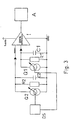
- the output load of an analog circuit A is its Output connected to the input of a driver stage I.
- the output of driver stage I is above a controllable coupling resistor RI to reference potential, its control input connected to the control output of a digital simulator DS is.
- a measuring element V for detecting the output voltage the analog circuit A.
- the digital simulator DS simulates by changing the coupling resistance RI different output loads for the Analog circuit A.
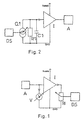
- FIG. 2 is a circuit arrangement according to the invention shown to simulate the input load of an analog circuit.
- a parallel circuit is connected to the input of a driver stage I. from a controllable current source Q1, a resistor R1 and a capacitance C1 connected.
- the control output a digital simulator DS is the controllable at the control input Power source Q1 connected.
- the output of the driver stage I is connected to the input of the analog circuit A.
- the digital simulator DS controls real-world simulations the controllable current source Q1.
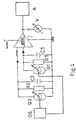
- 3 is an embodiment of the invention to simulate the input or output load of an analog circuit shown.
- FIG. 3 has the same structure as the exemplary embodiment shown in FIG. 2, is however characterized by a parallel connection a second controllable current source Q2 a second resistor R2 and a second capacitor C2 are added to the ENABLE input of driver stage I is connected.
- the control input the current source Q2 is with a second control output of the digital simulator DS connected.
- the digital simulator simulates DS by turning on the power source Q2 and controlling the Current source Q1 different input loads for the analog circuit A.
- the output of the analog circuit A connected to the output of driver stage I the Driver stage I switched off by the digital simulator DS.
- FIG. 4 is a further exemplary embodiment according to the invention to simulate the input or output load of a Analog circuit shown.
- FIG. 4 has the same structure as the embodiment Fig. 3.
- To detect the output voltage of the analog circuit A lies between the output of driver stage I and the reference potential a measuring element V.
- driver stage I CMOS inverter stage or a so-called default driver provided.
- the coupling to the analog circuit is preferably carried out via an RC link.
- the invention is characterized by the advantage that it also the simulation of the input or output load of an analog circuit sufficiently critical with critical input signals performs so additional simulations don't are more needed.
Landscapes
- Engineering & Computer Science (AREA)
- General Engineering & Computer Science (AREA)
- Physics & Mathematics (AREA)
- General Physics & Mathematics (AREA)
- Environmental & Geological Engineering (AREA)
- Logic Circuits (AREA)
- Tests Of Electronic Circuits (AREA)
Claims (8)
- Ensemble circuit pour simuler la charge de sortie d'un circuit analogique (A),
caractérisé en ce que
la sortie du circuit analogique (A) est reliée à l'entrée d'un étage de puissance (I), un élément (V) de mesure se trouve entre l'entrée de l'étage de puissance (I) et le potentiel de référence pour l'acquisition de la tension de sortie du circuit analogique (A), et entre la sortie de l'étage de puissance (I) et le potentiel de référence se trouve une résistance de couplage pilotable (RI) dont l'entrée de commande est reliée avec la sortie de commande d'un simulateur numérique (DS). - Ensemble circuit pour simuler la charge d'entrée d'un circuit analogique (A),
caractérisé en ce que
la sortie d'un étage de puissance (I) est reliée à l'entrée du circuit analogique (A), à l'entrée de l'étage de puissance (I) on a un circuit parallèle composé d'une première source pilotable de courant ou de tension (Q1), d'une première résistance (R1) et d'une première capacité (C1), et l'entrée de commande de la première source pilotable de courant ou de tension (Q1) est reliée avec la première sortie de commande d'un simulateur numérique (DS). - Ensemble circuit selon la revendication 2,
caractérisé en ce qu'
à l'entrée ENABLE de l'étage de puissance (I) est relié un circuit parallèle composé d'une deuxième source pilotable de courant ou de tension (Q2), d'une deuxième résistance (R2) et d'une deuxième capacité (C2), et l'entrée de commande de la deuxième source pilotable de courant ou de tension (Q2) est reliée avec la deuxième sortie de commande d'un simulateur numérique (DS). - Ensemble circuit selon la revendication 3,
caractérisé en ce qu'
un élément de mesure (V) se trouve entre la sortie de l'étage de puissance (I) et le potentiel de référence. - Ensemble circuit selon la revendication 1, 2, 3, ou 4,
caractérisé en ce que
l'étage de puissance (I) est constitué en tant qu'étage inverseur. - Ensemble circuit selon la revendication 5,
caractérisé en ce que
l'étage de puissance (I) est réalisé en technique CMOS. - Ensemble circuit selon la revendication 5 ou 6,
caractérisé en ce qu'
un « default driver », étage de puissance par défaut, est prévu pour l'étage de puissance (I). - Ensemble circuit selon l'une quelconque des revendications précédentes 2 à 7,
caractérisé en ce que
des cellules RC sont prévues dans le circuit analogique (A) pour le découplage.
Applications Claiming Priority (3)
| Application Number | Priority Date | Filing Date | Title |
|---|---|---|---|
| DE10001154A DE10001154A1 (de) | 2000-01-13 | 2000-01-13 | Schaltungsanordnung zur Simulation der Eingangs- oder Ausganslast einer Analogschaltung |
| DE10001154 | 2000-01-13 | ||
| PCT/EP2001/000169 WO2001051938A1 (fr) | 2000-01-13 | 2001-01-09 | Ensemble circuit pour simuler la charge d'entree ou de sortie d'un circuit analogique |
Publications (2)
| Publication Number | Publication Date |
|---|---|
| EP1247112A1 EP1247112A1 (fr) | 2002-10-09 |
| EP1247112B1 true EP1247112B1 (fr) | 2004-08-04 |
Family
ID=7627395
Family Applications (1)
| Application Number | Title | Priority Date | Filing Date |
|---|---|---|---|
| EP01907421A Expired - Lifetime EP1247112B1 (fr) | 2000-01-13 | 2001-01-09 | Ensemble circuit pour simuler la charge d'entree ou de sortie d'un circuit analogique |
Country Status (4)
| Country | Link |
|---|---|
| US (1) | US7096168B2 (fr) |
| EP (1) | EP1247112B1 (fr) |
| DE (2) | DE10001154A1 (fr) |
| WO (1) | WO2001051938A1 (fr) |
Families Citing this family (3)
| Publication number | Priority date | Publication date | Assignee | Title |
|---|---|---|---|---|
| DE10043905A1 (de) * | 2000-09-06 | 2002-03-14 | Infineon Technologies Ag | Stromkopplung bei der gemischten Simulation von Schaltungen |
| US7952395B2 (en) | 2009-10-13 | 2011-05-31 | King Fahd University Of Petroleum And Minerals | Universal CMOS current-mode analog function synthesizer |
| US20170024504A1 (en) * | 2015-07-22 | 2017-01-26 | Texas Instruments Incorporated | Logical to Multi-Variable-Record Connect Element to Interface Logical Signals Between Analog and Digital Simulations |
Family Cites Families (13)
| Publication number | Priority date | Publication date | Assignee | Title |
|---|---|---|---|---|
| US3631232A (en) * | 1969-10-17 | 1971-12-28 | Xerox Corp | Apparatus for simulating the electrical characteristics of a network |
| US3728616A (en) * | 1971-02-02 | 1973-04-17 | Western Electric Co | Continuity testing apparatus utilizing a plurality of paired resistors |
| US3916306A (en) * | 1973-09-06 | 1975-10-28 | Ibm | Method and apparatus for testing high circuit density devices |
| US4002974A (en) * | 1975-11-13 | 1977-01-11 | Bell Telephone Laboratories, Incorporated | Method and apparatus for testing circuits |
| US4158808A (en) * | 1977-08-18 | 1979-06-19 | The Valeron Corporation | Load source simulator |
| US4835726A (en) * | 1986-06-26 | 1989-05-30 | University Of Toronto Innovations Foundation | Apparatus for analog simulation of a circuit |
| US4712058A (en) * | 1986-07-22 | 1987-12-08 | Tektronix, Inc. | Active load network |
| US5196788A (en) * | 1991-07-03 | 1993-03-23 | The United States Of America As Represented By The Secretary Of The Navy | Self-contained functional test apparatus for modular circuit cards |
| GB2274716A (en) * | 1992-09-22 | 1994-08-03 | Mistrock Microsystems Limited | Circuit tester |
| US6480817B1 (en) * | 1994-09-01 | 2002-11-12 | Hynix Semiconductor, Inc. | Integrated circuit I/O pad cell modeling |
| JPH08288462A (ja) | 1995-04-14 | 1996-11-01 | Mitsubishi Electric Corp | 半導体集積回路装置 |
| US5945822A (en) * | 1996-09-05 | 1999-08-31 | Advantest Corporation | Programmable load circuit |
| DE19736197C1 (de) | 1997-08-20 | 1999-03-04 | Siemens Ag | Integrierte Schaltung mit Kondensatoren |
-
2000
- 2000-01-13 DE DE10001154A patent/DE10001154A1/de not_active Ceased
-
2001
- 2001-01-09 WO PCT/EP2001/000169 patent/WO2001051938A1/fr not_active Ceased
- 2001-01-09 DE DE50103092T patent/DE50103092D1/de not_active Expired - Lifetime
- 2001-01-09 EP EP01907421A patent/EP1247112B1/fr not_active Expired - Lifetime
-
2002
- 2002-07-15 US US10/195,731 patent/US7096168B2/en not_active Expired - Lifetime
Also Published As
| Publication number | Publication date |
|---|---|
| US7096168B2 (en) | 2006-08-22 |
| WO2001051938A1 (fr) | 2001-07-19 |
| EP1247112A1 (fr) | 2002-10-09 |
| DE10001154A1 (de) | 2001-07-26 |
| DE50103092D1 (de) | 2004-09-09 |
| US20030004700A1 (en) | 2003-01-02 |
Similar Documents
| Publication | Publication Date | Title |
|---|---|---|
| DE60100109T2 (de) | Umschaltbare Testschaltung für asymmetrischen und differentiellen Abschluss | |
| DE69016947T2 (de) | Auf einem Substrat integriertes Prüfsystem und Verfahren zur Nutzung dieses Prüfsystems. | |
| DE69429741T2 (de) | Analoge, selbstständige Prüfbusstruktur zum Testen integrierter Schaltungen auf einer gedruckten Leiterplatte | |
| DE2905271A1 (de) | Integrierte schaltungsanordnung in mos-technik mit feldeffekttransistoren | |
| DE3427986A1 (de) | Schaltungsanordnung zur ansteuerung von fluessigkristall-anzeigen | |
| DE3020107A1 (de) | Ueberwachungseinrichtung fuer einen lc-filterkreis an einem wechselspannungsnetz | |
| DE3885188T2 (de) | Elektrische Schaltung mit Verwendungsmöglichkeit in einem A/D-Wandler. | |
| DE2706428A1 (de) | Fensterkomparatorschaltung | |
| EP1247112B1 (fr) | Ensemble circuit pour simuler la charge d'entree ou de sortie d'un circuit analogique | |
| CH684665A5 (de) | MOSFET-gesteuerter Vervielfacher. | |
| DE4434792C1 (de) | Integrierte, in einem ersten und einem zweiten Betriebsmodus betreibbare Schaltungsanordnung | |
| DE2821812A1 (de) | Schaltungsanordnung zur potentialgetrennten uebertragung digitaler und analoger signale | |
| DE3412734A1 (de) | Schaltungsanordnung ..., insbesondere namurverstaerker | |
| DE4200935C1 (en) | Single power supply for multiple micro controlled A=D converters - has isolating switch stages coupled to output of DC=DC converter for connection to multiple A=D converters and amplifiers | |
| EP1983348A1 (fr) | Circuit pour mesurer, limiter et commuter un courant de charge | |
| DE29514423U1 (de) | EMV-Kompaktsensor | |
| WO2001014895A1 (fr) | Circuit et procede d'evaluation de capacites | |
| DE60019868T2 (de) | Galvanisch isolierende Schaltung | |
| DE3938459A1 (de) | Schaltungsanordnung zur kompensation von impulslaengenveraenderungen | |
| DE102023127259A1 (de) | Steuergerät mit wenigstens einer Schnittstelle für einen Sensor und Anordnung aus diesem Steuergerät und dem Sensor, der über eine Leitung an die Schnittstelle des Steuergerätes angeschlossen ist | |
| DE3305627C2 (de) | Schaltungsanordnung zur Überwachung des Arbeitsbereiches eines Operationsverstärkers | |
| DE4124474C2 (de) | Schaltungsanordnung zur Prüfung einphasiger Elektrizitätszähler mit galvanisch verbundenem Strom- und Spannungspfad | |
| DE4321014A1 (de) | Verfahren und Schaltung zum Schutz von Eingängen integrierter Schaltkreise gegen Übersprechen | |
| EP0446639B1 (fr) | Convertisseur analogique numérique parallèle | |
| WO2016078916A1 (fr) | Dispositif de mesure d'une grandeur électrique |
Legal Events
| Date | Code | Title | Description |
|---|---|---|---|
| PUAI | Public reference made under article 153(3) epc to a published international application that has entered the european phase |
Free format text: ORIGINAL CODE: 0009012 |
|
| 17P | Request for examination filed |
Effective date: 20020423 |
|
| AK | Designated contracting states |
Kind code of ref document: A1 Designated state(s): AT BE CH CY DE DK ES FI FR GB GR IE IT LI LU MC NL PT SE TR |
|
| 17Q | First examination report despatched |
Effective date: 20030113 |
|
| GRAP | Despatch of communication of intention to grant a patent |
Free format text: ORIGINAL CODE: EPIDOSNIGR1 |
|
| GRAS | Grant fee paid |
Free format text: ORIGINAL CODE: EPIDOSNIGR3 |
|
| GRAA | (expected) grant |
Free format text: ORIGINAL CODE: 0009210 |
|
| AK | Designated contracting states |
Kind code of ref document: B1 Designated state(s): DE FR GB IT |
|
| PG25 | Lapsed in a contracting state [announced via postgrant information from national office to epo] |
Ref country code: IT Free format text: LAPSE BECAUSE OF FAILURE TO SUBMIT A TRANSLATION OF THE DESCRIPTION OR TO PAY THE FEE WITHIN THE PRESCRIBED TIME-LIMIT;WARNING: LAPSES OF ITALIAN PATENTS WITH EFFECTIVE DATE BEFORE 2007 MAY HAVE OCCURRED AT ANY TIME BEFORE 2007. THE CORRECT EFFECTIVE DATE MAY BE DIFFERENT FROM THE ONE RECORDED. Effective date: 20040804 Ref country code: GB Free format text: LAPSE BECAUSE OF FAILURE TO SUBMIT A TRANSLATION OF THE DESCRIPTION OR TO PAY THE FEE WITHIN THE PRESCRIBED TIME-LIMIT Effective date: 20040804 |
|
| REG | Reference to a national code |
Ref country code: GB Ref legal event code: FG4D Free format text: NOT ENGLISH |
|
| REG | Reference to a national code |
Ref country code: IE Ref legal event code: FG4D Free format text: GERMAN |
|
| REF | Corresponds to: |
Ref document number: 50103092 Country of ref document: DE Date of ref document: 20040909 Kind code of ref document: P |
|
| GBT | Gb: translation of ep patent filed (gb section 77(6)(a)/1977) |
Effective date: 20050216 |
|
| REG | Reference to a national code |
Ref country code: IE Ref legal event code: FD4D |
|
| ET | Fr: translation filed | ||
| PLBE | No opposition filed within time limit |
Free format text: ORIGINAL CODE: 0009261 |
|
| STAA | Information on the status of an ep patent application or granted ep patent |
Free format text: STATUS: NO OPPOSITION FILED WITHIN TIME LIMIT |
|
| 26N | No opposition filed |
Effective date: 20050506 |
|
| REG | Reference to a national code |
Ref country code: FR Ref legal event code: PLFP Year of fee payment: 16 |
|
| PGFP | Annual fee paid to national office [announced via postgrant information from national office to epo] |
Ref country code: DE Payment date: 20160317 Year of fee payment: 16 |
|
| PGFP | Annual fee paid to national office [announced via postgrant information from national office to epo] |
Ref country code: FR Payment date: 20160121 Year of fee payment: 16 Ref country code: GB Payment date: 20160120 Year of fee payment: 16 |
|
| REG | Reference to a national code |
Ref country code: DE Ref legal event code: R119 Ref document number: 50103092 Country of ref document: DE |
|
| GBPC | Gb: european patent ceased through non-payment of renewal fee |
Effective date: 20170109 |
|
| REG | Reference to a national code |
Ref country code: FR Ref legal event code: ST Effective date: 20170929 |
|
| PG25 | Lapsed in a contracting state [announced via postgrant information from national office to epo] |
Ref country code: FR Free format text: LAPSE BECAUSE OF NON-PAYMENT OF DUE FEES Effective date: 20170131 |
|
| PG25 | Lapsed in a contracting state [announced via postgrant information from national office to epo] |
Ref country code: GB Free format text: LAPSE BECAUSE OF NON-PAYMENT OF DUE FEES Effective date: 20170109 Ref country code: DE Free format text: LAPSE BECAUSE OF NON-PAYMENT OF DUE FEES Effective date: 20170801 |