EP1246367A2 - Integrierte Halbleiterschaltung und Verfahren zu deren Herstellung - Google Patents
Integrierte Halbleiterschaltung und Verfahren zu deren Herstellung Download PDFInfo
- Publication number
- EP1246367A2 EP1246367A2 EP02005652A EP02005652A EP1246367A2 EP 1246367 A2 EP1246367 A2 EP 1246367A2 EP 02005652 A EP02005652 A EP 02005652A EP 02005652 A EP02005652 A EP 02005652A EP 1246367 A2 EP1246367 A2 EP 1246367A2
- Authority
- EP
- European Patent Office
- Prior art keywords
- circuit
- interconnect
- impedance
- semiconductor integrated
- integrated circuit
- Prior art date
- Legal status (The legal status is an assumption and is not a legal conclusion. Google has not performed a legal analysis and makes no representation as to the accuracy of the status listed.)
- Ceased
Links
Images


Classifications
-
- H10W44/20—
-
- H—ELECTRICITY
- H03—ELECTRONIC CIRCUITRY
- H03K—PULSE TECHNIQUE
- H03K19/00—Logic circuits, i.e. having at least two inputs acting on one output; Inverting circuits
- H03K19/003—Modifications for increasing the reliability for protection
- H03K19/00346—Modifications for eliminating interference or parasitic voltages or currents
- H03K19/00353—Modifications for eliminating interference or parasitic voltages or currents in bipolar transistor circuits
-
- H—ELECTRICITY
- H03—ELECTRONIC CIRCUITRY
- H03K—PULSE TECHNIQUE
- H03K19/00—Logic circuits, i.e. having at least two inputs acting on one output; Inverting circuits
- H03K19/0175—Coupling arrangements; Interface arrangements
- H03K19/018—Coupling arrangements; Interface arrangements using bipolar transistors only
- H03K19/01825—Coupling arrangements, impedance matching circuits
- H03K19/01831—Coupling arrangements, impedance matching circuits with at least one differential stage
-
- H—ELECTRICITY
- H03—ELECTRONIC CIRCUITRY
- H03K—PULSE TECHNIQUE
- H03K19/00—Logic circuits, i.e. having at least two inputs acting on one output; Inverting circuits
- H03K19/02—Logic circuits, i.e. having at least two inputs acting on one output; Inverting circuits using specified components
- H03K19/08—Logic circuits, i.e. having at least two inputs acting on one output; Inverting circuits using specified components using semiconductor devices
- H03K19/082—Logic circuits, i.e. having at least two inputs acting on one output; Inverting circuits using specified components using semiconductor devices using bipolar transistors
- H03K19/086—Emitter coupled logic
-
- H10W20/495—
-
- H—ELECTRICITY
- H03—ELECTRONIC CIRCUITRY
- H03F—AMPLIFIERS
- H03F2203/00—Indexing scheme relating to amplifiers with only discharge tubes or only semiconductor devices as amplifying elements covered by H03F3/00
- H03F2203/45—Indexing scheme relating to differential amplifiers
- H03F2203/45722—Indexing scheme relating to differential amplifiers the LC comprising one or more source followers, as post buffer or driver stages, in cascade in the LC
Definitions
- the present invention relates to a semiconductor integrated circuit and more particularly to a semiconductor integrated circuit for quickly processing broadband data signals, and a manufacturing method such a semiconductor integrated circuit.
- High performance of an element can be obtained by basically reducing the size of the element.
- a field effect transistor by reducing a gate length
- a bipolar transistor by reducing a base thickness and an emitter width
- a current gain cut-off frequency is improved and by reducing peripheral parts, a parasitic capacitance is reduced, thereby realizing more powerful transistors.
- a conventional emitter coupled logic (ECL) circuit as a fundamental logic circuit using bipolar transistors.
- This ECL circuit comprises a current switch circuit (differential circuit) and an emitter follower circuit.
- the current switch circuit is a circuit that emitters of a pair of driving transistors 603 and 604 are connected in common. Both of the emitters of the driving transistors 603 and 604 are connected to a collector of constant current source transistor 607 in common. Collectors of the transistors 603 and 604 are connected in common to a connection line via a pair of load resistors 605 and 606, respectively and a high level power supply terminal 608 is coupled to the connection line.
- the emitter follower circuit comprises a pair of input transistors 612 and 613 and a pair of load resistors 614 and 615.
- the bases of the two input transistors 612 and 613 are connected to the collectors of the two drive transistors 603 and 604, respectively.
- the emitters of the two input transistors 612 and 613 are commonly linked to the emitter of the constant current source transistor 607 via the respective load resistors 614 and 615 and a connection line and this connection line is coupled to a low level power supply terminal 609.
- the collectors of the two input transistors 612 and 613 are connected in common to the connection line coupled to the high level power supply terminal 608.
- Two output terminals 616 and 617 of the ELC circuit are connected to the respective connection lines connecting the emitters of the input transistors 612 and 613 and the load resistors 614 and 615, respectively.
- the high integration is realized by shortening the interconnect between the current switch circuit and the emitter follower circuit and the interconnect within these two circuits in order to reduce interconnect delay time are shortened to intend the high integration. As a result, the high speed operation of the ECL circuit can be realized.
- L is inductance of interconnect and C is capacitance of the interconnect.
- a circuit using air-bridge interconnect having a low parasitic capacitance is known.
- an inductor component of the interconnect distortion occurs in the data signal even within the circuit.
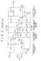
- Fig. 2 there is shown a two-stage ECL circuit constituting two current switch circuits and four emitter follower circuits.
- the two-stage ECL circuit includes the first ECL circuit having two inputs and outputs shown in Fig. 1 and the second ECL circuit having a similar construction to the first ECL circuit.
- the outputs of the first ECL circuit are input to the second ECL circuit via two interconnects 638 and 639.
- the same members as those shown in Fig. 1 are designated by the same numerals and thus the explanation thereof can be omitted.
- the second ECL circuit includes one current switch circuit and one emitter follower circuit in the same manner as the first ECL circuit.
- the emitter follower circuit of the first ECL circuit is called the first stage emitter follower circuit and the emitter follower circuit of the second ECL circuit is the second stage emitter follower circuit.
- the second stage emitter follower circuit includes a pair of input transistors 616 and 617 and a pair of load resistors 618 and 619. More specifically, the base of the input transistor 616 is coupled to the connection line connecting the emitter of the input transistor 612 of the first emitter follower circuit and the load resistor 614 via the interconnect 638, and the base of the input transistor 617 is coupled with to the connection line connecting the emitter of the input transistor 613 of the first emitter follower circuit and the load resistor 615 via the interconnect 639.
- the emitters of the two input transistors 616 and 617 are connected in common to a connection line via the respective load resistors 618 and 619, and this connection line is coupled to the low level power supply terminal 609.
- the collectors of the two input transistors 618 and 619 are connected in common to a connection line to which the high level power supply terminal 608 is coupled.
- the current switch circuit of the second stage ECL circuit in the same manner as the first ECL circuit, includes a pair of drive transistors 623 and 624, a constant current source transistor 627 and a pair of load resistors 625 and 626.
- the emitters of the two drive transistors 623 and 624 are commonly coupled with the collector of the constant current source transistor 627.
- the base of the drive transistor 623 is connected to the connection line connecting the emitter of the input transistor 616 and the load resistor 618, and the base of the drive transistor 624 is connected to the connection line connecting the emitter of the input transistor 617 and the load resistor 619.
- the collectors of the two drive transistors 623 and 624 are connected in common to the connection line via the respective load resistors 625 and 626, and this connection line is coupled to the high level power supply terminal 608.
- the emitter of the constant current source transistor 627 is linked to the connection line to which the low level power supply terminal 609 is coupled.
- the current switch circuit and the emitter follower circuit are connected by the interconnect and the transistors and the resistors within the circuits are connected by the interconnect.
- the interconnects 638 and 639 coupling the first emitter follower circuit with the second emitter follower circuit will now be considered.
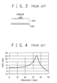
- Fig. 3 shows a cross sectional view of the interconnects 638 and 639 for coupling the first and the second emitter follower circuits of the conventional two-stage ECL circuit.
- the back surface of a semiconductor substrate on which the ECL circuit is formed, is an ground 630.
- a interconnecting layer of Au such as the interconnects 638 and 639 having a thickness of 1 ⁇ m and a width of 6 ⁇ m is formed on the ground 630 via a semiconductor layer 631 of a GaAs layer having a thickness of 120 ⁇ m.
- a interconnect length of the interconnecting layer is 500 ⁇ m.
- Fig. 4 there is shown a frequency characteristic of from DC to 50 GHz gain of the aforementioned two-stage ECL circuit.
- the interconnect length between the first emitter follower circuit and the second emitter follower circuit is shorter than a wavelength of a quarter of 50 GHz, since the length of the interconnects 638 and 639 is 500 ⁇ m, it is found that the gain peaking around 27 GHz.
- the characteristic impedance of the shortened interconnect is necessarily considered.
- the characteristic impedance of such a interconnect has not been considered conventionally, when the frequency becomes high, the distortion of the data signal or the gain peaking of the frequency characteristic occurs and the data signal cannot be propagated well.
- a high frequency differential output circuit includes a differential pair of field effect transistors and a constant current circuit of a field effect transistor, and further includes an inductive circuit for preventing a parasitic capacitance of the field effect transistor from affecting a bad influence to an impedance characteristic of an output terminal by an inductive impedance of the inductive circuit.
- additional interconnect for connecting the inductive circuit to the field effect transistor is necessary and it becomes disadvantageous to realize high integration and low cost.
- a reflection reduction circuit including a first resistor connected between the interconnect and a power source potential and a second resistor connected between the interconnect and an earth potential is placed near the impedance discontinuously changing part of the interconnect.
- the reflection of the signal at the discontinuous part of the interconnect can be reduced, but the aforementioned problem of the reflection caused by the impedance mismatching between the interconnect and its front stage circuit or between the interconnect and its rear stage circuit cannot be solved.
- a semiconductor integrated circuit comprising: a first circuit having an output terminal; a second circuit having an input terminal; and interconnect for connecting the output terminal of the first circuit and the input terminal of the second circuit, a characteristic impedance of the interconnect matching an output impedance of the first circuit in a predetermined frequency range.
- the semiconductor integrated circuit of the present invention can further comprise an impedance converter circuit connected between the interconnect and the output terminal of the first circuit.
- a semiconductor integrated circuit comprising: a first circuit having an output terminal; a second circuit having an input terminal; and interconnect for connecting the output terminal of the first circuit and the input terminal of the second circuit, a characteristic impedance of the interconnect matching an input impedance of the second circuit in a predetermined frequency range.
- the semiconductor integrated circuit of the present invention can further comprise an impedance converter circuit connected between the interconnect and the input terminal of the second circuit.
- a semiconductor integrated circuit comprising: a first circuit having an output terminal; a second circuit having an input terminal; and interconnect for connecting the output terminal of the first circuit and the input terminal of the second circuit, a characteristic impedance of the interconnect matching both an output impedance of the first circuit and an input impedance of the second circuit in a predetermined frequency range.
- the semiconductor integrated circuit of the present invention can further comprise a first impedance converter circuit connected between the interconnect and the output terminal of the first circuit and a second impedance converter circuit connected between the interconnect and the input terminal of the second circuit.
- the predetermined frequency range includes a frequency that distortion is caused in a waveform of a data signal propagating the interconnect by either an inductor or capacitance of the interconnect.
- the characteristic impedance of the interconnect is determined so that an eye opening ratio representing a rate of an amplitude size of an eye pattern of a data signal propagating the interconnect to the amplitude size of the eye pattern of the data signal input to the output terminal of the first circuit may be larger than a predetermined value.
- the interconnect, the first circuit and the second circuit are formed on a same semiconductor substrate to obtain the semiconductor integrated circuit having a monolithic structure.
- a method for producing a semiconductor integrated circuit comprising the steps of forming a first circuit having an output terminal and a second circuit having an input terminal on a semiconductor substrate; and forming interconnect for connecting the output terminal of the first circuit and the input terminal of the second circuit, a characteristic impedance of the interconnect being determined so that an eye opening ratio representing a rate of an amplitude size of an eye pattern of a data signal propagating the interconnect to the amplitude size of the eye pattern of the data signal input to the output terminal of the first circuit may be larger than a predetermined value.
- an output impedance of the first circuit, an input impedance of the second circuit, the characteristic impedance of the interconnect and the eye opening ratio are R1, R2, Z0 and M, respectively, these values can satisfy the following formula in a frequency range for the data signal propagating the interconnect.
- the method for producing a semiconductor integrated circuit of the present invention can further comprise forming an impedance converter circuit connected between the interconnect and the output terminal of the first circuit, and it is assumed that the output impedance, converted by the impedance converter circuit, of the first circuit is R1.
- the method for producing a semiconductor integrated circuit of the present invention can further comprise forming an impedance converter circuit connected between the interconnect and the input terminal of the second circuit, and it is assumed that the input impedance, converted by the impedance converter circuit, of the second circuit is R2.
- a characteristic impedance of interconnect and an output impedance and an input impedance of circuits constituting a semiconductor integrated circuit can be known by calculations (simulation).
- the characteristic impedance of the interconnect can be calculated on the basis of its width, thickness, dielectric constant and the like.
- the characteristic impedance of the interconnect is adapted to match the output impedance of the first circuit, the input impedance of the second circuit, or both the output impedance and the input impedance of the first and the second circuits in a predetermined frequency range (the frequency that the distortion is caused in the waveform of the data signal propagating the interconnect by the inductor or capacitance of the interconnect, more specifically, the frequency of the order of GHz), and thus none of the distortion of the data signal and the gain peaking can be caused.
- the inductive circuit mentioned in the Japanese Patent Laid-open Publication No. 9-162653 is not necessary.
- the characteristic impedance of the interconnect is set so that an eye opening ratio may be larger than a predetermined value, the occurrence of the distortion in the data signal waveform owing to the reflection can be exactly prevented.
- an output impedance of a first circuit, an input impedance of a second circuit, a characteristic impedance of interconnect and an eye opening ratio of a data signal (pulse signal) propagating the interconnect are R1, R2, Z0 and M, respectively.
- the formula (i) mainly restricts a size of overshoot, caused by the reflection, of the data signal waveform and the formula (ii) mainly restricts a size of undershoot, caused by the reflection, of the data signal waveform.
- an open state of an aperture of an eye pattern of the data signal waveform can be set to a certain range by using the formulas (i) and (ii) so that the data signal may be propagated. Hence, the occurrence of the distortion of the data signal waveform owing to the reflection can be exactly prevented.
- FIG. 7 there is shown a semiconductor integrated circuit of an emitter coupled logic (ECL) circuit according to the first embodiment of the present invention.
- ECL emitter coupled logic
- the current switch circuit includes a pair of drive circuits 103 and 104, a pair of load resistors 105 and 106 and a constant current source transistor 109. More specifically, two input terminals 101 and 102 are connected to the bases of the two drive transistors 103 and 104 and the emitters of the two drive transistors 103 and 104 are commonly coupled with the collector of the constant current source transistor 109. The collectors of the two drive transistors 103 and 104 are connected in common to a connection line via the respective load resistors 105 and 106 and this connection line is coupled to a high level power supply terminal 116. Two output terminals 107 and 108 of this current switch circuit are connected to the respective connection lines connecting the collectors of the two drive transistors 103 and 104 and the two load resistors 105 and 106, respectively.
- the emitter follower circuit includes a pair of input transistors 112 and 113 and a pair of load resistors 114 and 115. That is, two input terminals 110 and 111 are coupled with the bases of the two input transistors 112 and 113, respectively.
- the emitters of the two input transistors 112 and 113 are commonly linked to the emitter of the constant current source transistor 109 via the respective load resistors 114 and 115 and a connection line coupled to a low level power supply terminal 117.
- the collectors of the two input transistors 112 and 113 are connected in common to the connection line to which the high level power supply terminal 116 is coupled.
- the two output terminals 107 and 108 of the current switch circuit are connected to the two input terminals 110 and 111 of the emitter follower circuit via two interconnects (wirings) 118 and 119, respectively.
- the two interconnects 118 and 119 connect the collectors of the two drive transistors 103 and 104 and the bases of the two input transistors 112 and 113 via the two output terminals 107 and 108 of the current switch circuit and the two input terminals 110 and 111 of the emitter follower circuit.
- a matching between an output impedance of the current switch circuit and a characteristic impedance of the interconnect 118 and 110 is taken so that an eye opening ratio which represents a rate of an amplitude size of an eye pattern of a data signal propagating the interconnect 118 and 110 to the amplitude size of the eye pattern of the data signal input to the output terminal 107 of the current switch circuit, may be larger than a predetermined value.
- an output impedance of the current switch circuit, an input impedance of the emitter follower circuit, a characteristic impedance of the interconnect and an eye opening ratio of a data signal (pulse signal) propagating the interconnect are R1, R2, Z0 and M, respectively.
- FIG. 8 there is shown an output characteristic such as relationship between an output impedance and a frequency at the output terminals 107 and 108 of the current switch circuit of the ECL circuit shown in Fig. 7.
- the load resistors 105 and 106 having a resistance value of 30 ⁇ are used in the current switch circuit and the output impedance R1 of the current switch circuit is 30 ⁇ + j0 ⁇ 27 ⁇ - j7 ⁇ ((30 +j0) ⁇ (27- j7) ⁇ ) in the frequency range from DC to 100 GHz.
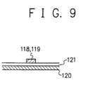
- Fig. 9 there is shown a structure of the interconnects 118 and 119 for connecting the current switch circuit and the emitter follower circuit of the ECL circuit shown in Fig. 7.
- the interconnects 118 and 119 as the second interconnecting layer (strip line) having a thickness of 1 ⁇ m and a width of 4 ⁇ m are formed on an ground 120 as the first interconnecting layer (flat conductor plate) via an interlayer insulating film 121 of SiO 2 having a thickness of 1 ⁇ m.
- This interconnect structure is a micro strip line interconnect and its characteristic impedance Z 0 is approximately 28 ⁇ .
- the characteristic impedance Z 0 of the interconnect 118 and 119 is 28 ⁇ , the real number part of the left side of the formula (3) becomes 0.034 ⁇ 0.018 and the condition of the formula (1) is satisfied. In the same way, the real number part of the left side of the formula (4) becomes 0.001 ⁇ 0.0003 and the condition of the formula (2) is satisfied.
- the characteristic impedance of the interconnects 118 and 119 matches the output impedance of the current switch circuit.
- the interconnect length of the interconnects 118 and 119 is long such as 1 mm, no gain peaking occurs in the frequency characteristic and no distortion arises in the data signal. Hence, the amplitude and the propagation of the data signal can be correctly carried out.
- the characteristic impedance of the interconnects 118 and 119 still does not match the input impedance of the emitter follower circuit at its input terminals 110 and 111.
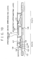
- Fig. 10 is a cross sectional view showing a construction of the semiconductor integrated circuit of the emitter coupled logic circuit shown in Fig. 7.
- a subcollector layer 123, a collector layer 124, a base layer 125 and an emitter layer 126 are successively formed in this order.
- each of an emitter electrode 127, a base electrode 128 and a collector electrode 129 of transistors are formed by using a lithography using a photo-resist film, an etching and an ohmic electrode formation technique.
- the drive transistor 103 or 104 is separated from the input transistor 112 or 113 by an isolation 130.
- a Ti/Pt/Au layer as a first interconnecting layer is formed by a sputtering method and an ion milling method.
- This first interconnecting layer is the ground 120 shown in Fig. 9. While this first interconnecting layer is formed, a resistor 131 is also formed. This resistor 131 is the resistor 105 or 106 shown in Fig. 7.
- the interlayer insulating film (SiO 2 ) is deposited again in thickness of 1 ⁇ m and thereafter a second interconnecting layer of the Ti/Pt/Au layer or an Au layer is formed in the same manner as the first interconnecting layer or by an Au plating method.
- This second interconnecting layer is the interconnect 118 or 119 shown in Fig. 7 and the interlayer insulating film deposited in thickness of 1 ⁇ m is the interlayer insulating film 121 shown in Fig. 9.
- the width and the thickness of the micro strip line are determined so that the characteristic impedance of the interconnect may match the output impedance of the current switch circuit, the input impedance of the emitter follower circuit, or both the output impedance of the current switch circuit and the input impedance of the emitter follower circuit.
- the width and the thickness of the micro strip line are determined so that at least one of the two formulas (1) and (2) may be satisfied.
- a semiconductor integrated circuit having a monolithic structure (interconnects and circuits are formed on a same semiconductor substrate) including the micro strip line interconnect shown in Fig. 9 can be produced.
- ECL circuit using the bipolar transistors has been described, the same effects and advantages can be obtained in an integrated circuit using other devices such as field effect transistors (FETs) of GaAs and/or MOS (metal oxide semiconductor) transistors.
- FETs field effect transistors
- MOS metal oxide semiconductor
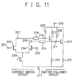
- FIG. 11 there is shown a semiconductor integrated circuit having an ECL circuit structure according to a second embodiment of the present invention.
- This ECL circuit includes a current switch circuit and an emitter follower circuit.
- the current switch circuit includes a pair of drive transistors 203 and 204 and a constant current source transistor 209. More specifically, the emitters of the drive transistors 203 and 204 are connected in common to the collector of the constant current transistor 209. Two input terminals 201 and 202 are connected to the bases of the drive transistors 203 and 204, respectively, and two output terminals 207 and 208 are linked to the collectors of the drive transistors 203 and 204, respectively.
- the emitter follower circuit includes a pair of input transistors 212 and 213 and a pair of load resistors 214 and 215. That is, two input terminals 210 and 211 are coupled with the bases of the input transistors 212 and 213, respectively.
- the collectors of the two input transistors 212 and 213 are connected to their own bases via two load resistors 205 and 206, respectively. Further, the collectors of the two input transistors 212 and 213 are connected in common to a connection line coupled to a high level power supply terminal 216.
- the emitters of the two input transistors 212 and 213 are commonly linked to the emitter of the constant current transistor 209 via the respective load resistors 214 and 215 and a connection line and this connection line is coupled to a low level power supply terminal 217.
- the two load resistors 205 and 206 are the load resistors of the current switch circuit.
- the two output terminals 207 and 208 of the current switch circuit are coupled with the two input terminals 210 and 211 of the emitter follower circuits via the interconnects 218 and 219, respectively. That is, the current switch circuit and the emitter follower circuit are connected by the interconnects 218 and 219 arranged between the two drive transistors 203 and 204 and the two load resistors 205 and 206 of the current switch circuit.
- a matching is made between a characteristic impedance of the interconnects 218 and 219 and an input impedance of the emitter follower circuit so that an eye opening ratio may be larger than a predetermined value.
- the load resistors 205 and 206 of the current switch circuit are directly connected to the input transistors 212 and 213 of the emitter follower circuit different from the first embodiment described above.
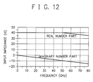
- Fig. 12 illustrates the input impedance at the input terminals 210 and 211 of the emitter follower circuit.
- the load resistors 205 and 206 having a resistance value of 40 ⁇ are used and the input impedance R 2 at the input terminals 210 and 211 of the emitter follower circuit is 40 ⁇ + j0 ⁇ 35 ⁇ - j15 ⁇ in the frequency range from DC to 80 GHz.
- Fig. 13 there is shown a structure of the interconnects 218 and 219 for connecting the drive transistors 203 and 204 and the load resistors 205 and 206 of the current switch circuit.
- the interconnects 218 and 219 as the second interconnecting layer (strip line) having a thickness of 1 ⁇ m and a width of 4 ⁇ m are formed on an ground 220 as the first interconnecting layer (flat conductor plate) via an interlayer insulating film 221 of SiO 2 having a thickness of 1.5 ⁇ m.
- This interconnect structure is a micro strip line interconnect and its characteristic impedance Z 0 is approximately 38 ⁇ .
- the characteristic impedance of the interconnects 218 and 219 matches the input impedance of the emitter follower circuit.
- the interconnect length of the interconnects 218 and 219 is as long as 500 ⁇ m, no gain peaking occurs in the frequency characteristic and no distortion arises in the data signal.
- the amplitude and the propagation of the data signal can be correctly performed.
- the characteristic impedance of the interconnects 218 and 219 still mismatches the output impedance of the current switch circuit at its output terminals 207 and 208.
- the matching is made between the characteristic impedance of the interconnect and the input impedance of the emitter follower circuit has been described in this embodiment by using the aforementioned formulas (1) and (2), the matching between the characteristic impedance of the interconnect and the output impedance of the current switch circuit and further the matching between the characteristic impedance of the interconnect and both the output impedance of the current switch circuit and the input impedance of the emitter follower circuit may be matched.
- the ECL circuit of this embodiment can be produced by using almost the same manufacturing process as the first embodiment described above and the width and the thickness of the micro strip line of the interconnect can be suitably determined so that at least one of the formulas (1) and (2) may be satisfied.
- ECL circuit using the bipolar transistors has been described, the same effects and advantages can be obtained in an integrated circuit using other devices such as the field effect transistors (FETs) of GaAs and the MOS transistors.
- FETs field effect transistors
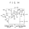
- FIG. 14 there is shown a semiconductor integrated circuit having an ECL circuit structure according to a third embodiment of the present invention.
- This ECL circuit further includes a pair of load resistors 325 and 326 of the current switch circuit besides the ECL circuit shown in Fig. 7.
- the same members as those shown in Fig. 7 are designated by the same numerals and thus the description thereof can be omitted.
- one ends of the two load resistors 325 and 326 are connected to the bases of the respective input transistors 112 and 113 of the emitter follower circuit and also to the respective input terminals 110 and 111 and the other ends of the two load resistors 325 and 326 are connected in common to the connection line to which the high level power supply terminal 116 is coupled.
- a matching between a characteristic impedance of the interconnects 118 and 119 and an input impedance of the emitter follower circuit and a matching between the characteristic impedance of the interconnects 118 and 119 and an output impedance of an emitter follower circuit are executed so that an eye opening ratio may be larger than a predetermined value.
- the load resistance value of the current switch circuit is determined by a parallel circuit of the resistors 105, 106, 325 and 326.
- the resistors 105, 106, 325, and 326 having a resistance value of 100 ⁇ are used in the current switch circuit and the load resistance value becomes 50 ⁇ .
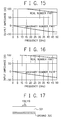
- Fig. 15 illustrates an input impedance of the current switch circuit on the input side of the interconnects 118 and 119 for connecting the current switch circuit and the emitter follower circuit of the ECL circuit shown in Fig. 14.
- the output impedance R1 of the current switch circuit is 100 ⁇ + j0 ⁇ 80 ⁇ - j38 ⁇ in the frequency range from DC to 50 GHz.
- Fig. 16 illustrates an input impedance of the emitter follower circuit on the output side of the interconnects 118 and 119 for connecting the current switch circuit and the emitter follower circuit of the ECL circuit shown in Fig. 14.
- the resistors 325 and 326 as a part of the whole load resistors of the current switch circuit are directly connected to the input transistors 112 and 113 of the emitter follower circuit in the same manner as the second embodiment described above, and the input impedance R2 of the emitter follower circuit is 100 ⁇ + j0 ⁇ 81 ⁇ - j35 ⁇ in the frequency range from DC to 50 GHz.
- Fig. 17 there is shown a structure of the interconnects 118 and 119 for connecting the current switch circuit and the emitter follower circuit.
- the interconnects (strip line) 118 and 119 of Au having a thickness of 1 ⁇ m and a width of 6 ⁇ m are formed on an ground 320 as the first interconnecting layer (flat conductor plate) via a semiconductor layer 321 of GaAs having a thickness of 80 ⁇ m.
- This interconnect structure is a micro strip line interconnect and its characteristic impedance Z 0 is approximately 100 Q .
- the necessary eye opening ratio M for the pulse signal propagating the interconnect is 0.8. Since both the right sides of the formulas (1) and (2) are 0.1, the real number part of the left side of the formula (1) becomes 0 ⁇ 0.006 and the real number part of the left side of the formula (2) becomes 0 ⁇ 0. As a result, both the conditions of the formulas (1) and (2) are satisfied.
- the characteristic impedance of the interconnects 118 and 119 matches both the output impedance of the current switch circuit and the input impedance of the emitter follower circuit.
- the ECL circuit of this embodiment can be produced by using almost the same producing process as the first embodiment described above and the width and the thickness of the micro strip line of the interconnect can be suitably determined so that both the formulas (1) and (2) may be satisfied.
- ECL circuit using the bipolar transistors has been described, the same effects and advantages can be obtained in an integrated circuit using other devices such as the field effect transistors (FETs) of GaAs and the MOS transistors.
- FETs field effect transistors
- the semiconductor integrated circuit includes a first emitter follower circuit and a second emitter follower circuit and further includes an impedance converter circuit using a resistor is placed at the output of the first emitter follower circuit.
- the first emitter follower circuit includes an input transistor 402 and a load resistor 403 and the second emitter follower circuit includes an input transistor 406 and a load resistor 407. More specifically, in the first emitter follower circuit, an input terminal 401 is connected to the base of the input transistor 402 and an output terminal 404 is connected to a connection line connecting the emitter of the input transistor 402 and the load resistor 403. In the second emitter follower circuit, an input terminal 405 is connected to the base of the input transistor 406 and an output terminal 408 is connected to a connection line connecting the emitter of the input transistor 406 and the load resistor 407.
- the collectors of the input transistors 402 and 406 are connected in common to a connection line coupled to a high level power supply terminal 409, and the emitters of the input transistors 402 and 406 are linked in common to a connection line via the respective load resistors 403 and 407 and this connection line is coupled to a low level power supply terminal 410.
- the impedance converter circuit includes a resistor 411. One end of the resistor 411 is connected to the output terminal of the first emitter follower circuit and the other end of the resistor 411 is coupled with an output terminal 412 of the impedance converter circuit. This output terminal 412 of the impedance converter circuit is linked to the input terminal 405 of the second emitter follower circuit via a interconnect 413 for coupling the first and the second emitter follower circuits.
- a matching is made between a characteristic impedance of the interconnect 413 and an output impedance, converted by the impedance converter circuit, of the first emitter follower circuit so that an eye opening ratio may be larger than a predetermined value.
- the interconnect 413 for coupling the first and the second emitter follower circuits has the same interconnect structure as the semiconductor substrate shown in Fig. 3. That is, the interconnect 413 of a interconnecting layer of Au having a thickness of 1 ⁇ m and a width of 6 ⁇ m is formed on an ground 630 via a semiconductor layer 631 of a GaAs layer having a thickness of 120 ⁇ m, and its characteristic impedance Z 0 is approximately 105 ⁇ .
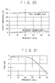
- Fig. 19 there is shown an output impedance of the first emitter follower circuit at output of the output terminal 404 and frequency.
- the output impedance of the first emitter follower circuit is 21 ⁇ + j0 ⁇ ⁇ 27 ⁇ + j8 ⁇ in the frequency range from DC to 50 GHz.
- the characteristic impedance of the interconnect 413 matches the output impedance of the first emitter follower circuit that the impedance converter circuit is connected to its output.
- the interconnect length of the interconnect 413 is long such as 500 ⁇ m, unwanted gain peaking does not occur in the frequency characteristic and no distortion arises in the data signal. Hence, the amplitude and the propagation of the data signal can be correctly carried out.
- the impedance converter circuit can be placed at the input of the second emitter follower circuit to execute the impedance matching between the interconnect 413 and the second emitter follower circuit in the same manner as described above.
- the input impedance, converted by the impedance converter circuit, of the second emitter follower circuit is R 2
- the matching between the characteristic impedance of the interconnect 413 and the input impedance, converted by the impedance converter circuit, of the second emitter follower circuit is conducted so as to satisfy the aforementioned formulas (3) and (2).
- the impedance matching between the interconnect and the first emitter follower circuit and between the interconnect and the second emitter follower circuit can be performed in the same manner as described above.
- An impedance converter circuit is placed between the first and the second emitter follower circuits.
- two impedance converter circuits are required, that is, a pair of impedance converter circuits are placed just before the pair of interconnects 638 and 639, respectively, for coupling the first and the second emitter follower circuits.
- a interconnect length of a resistor of each impedance converter circuit is 500 ⁇ m.
- Fig. 21 there is shown a frequency characteristic of gain of the two-stage ECL circuit shown in Fig. 2, to which the semiconductor integrated circuit shown in Fig. 18 is applied.
- the frequency-gain characteristic shown in Fig. 21 there is no gain peaking different from the frequency-gain characteristic shown in Fig. 4.
- Fig. 22 there is shown a waveform of an output data signal of the two-stage ECL circuit when a data signal having a pseudo-random pattern of 20 Gbit/s is input to the two-stage ECL circuit.
- the data signal having no error can be propagated.
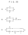
- Figs. 23(A), 23(B) and 23(C) show other impedance converter circuits to be used in the present invention.
- a first impedance converter circuit shown in Fig. 23(A) includes a resistor R and a capacitor C which are connected in parallel.
- a second impedance converter circuit shown in Fig. 23(B) includes a first resistor R 1 and a capacitor C which are connected in parallel and a second resistor R 2 .
- a third impedance converter circuit shown in Fig. 23(C) includes a capacitor C, a second resistor R 2 and a coil L which are linked in series and further includes a first resistor R 1 connected in parallel with the series of the capacitor C, the second resistor R 2 and the coil L.
- the semiconductor integrated circuit of this embodiment can be also produced by using almost the same producing process as the first embodiment described above and the width and the thickness of the micro strip line of the interconnect can be suitably determined so that at least one ofthe formulas (1) and (2) may be satisfied.
- the semiconductor integrated circuit includes first and second inverter circuits using complementary metal oxide semiconductor (CMOS) transistors and a interconnect 511 for coupling the first and the second inverter circuits.
- CMOS complementary metal oxide semiconductor
- the first inverter circuit includes an N type MOS (N-channel metal oxide semiconductor) transistor 502 and a P type MOS (P-channel metal oxide semiconductor) transistor 503.
- the second inverter circuit includes an N type MOS transistor 506 and a P type MOS transistor 507. More specifically, in the first inverter circuit, the gates of the N type MOS transistor 502 and the P type MOS transistor 503 are commonly coupled by a line connected to an input terminal 501. The drains of the N type MOS transistor 502 and the P type MOS transistor 503 are commonly coupled by a line connected to an output terminal 504. In the second inverter circuit, the gates of the N type MOS transistor 506 and the P type MOS transistor 507 are commonly coupled by a line connected to an input terminal 505.
- the drains of the N type MOS transistor 506 and the P TYPE MOS transistor 507 are commonly coupled by a line connected to an output terminal 508.
- the output terminal 504 of the first inverter circuit is coupled with the input terminal 505 of the second inverter circuit via the interconnect 511.
- a matching between a characteristic impedance of the interconnect 511 and an output impedance of the first inverter circuit is executed so that an eye opening ratio may be larger than a predetermined value.
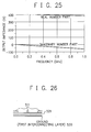
- FIG. 25 there is shown an output impedance of the first inverter circuit at its output terminal 504 with reference to a frequency.
- the output impedance R 1 of the first inverter circuit is 400 ⁇ + j0 ⁇ 387 ⁇ - j55 ⁇ in the frequency range from DC to 1 GHz.
- FIG. 26 there is shown a structure of the interconnect 511 for coupling the first and second inverter circuits of the semiconductor integrated circuit shown in Fig. 24.
- Acentral conductor 511a as a second interconnecting layer such as the interconnect 511 having a thickness of 0.4 ⁇ m and a width of 4 ⁇ m and grounds 511b as the second interconnecting layer, 20 ⁇ m apart from the central conductor 511a, are formed on an ground 520 as a first interconnecting layer (flat conductor plate) via an interlayer insulating film 521 of SiO 2 having a thickness of 0.4 ⁇ m, and its characteristic impedance Z 0 is approximately 390 ⁇ .
- the necessary eye opening ratio M for the pulse signal propagating the interconnect is 0.8. Since both the right sides of the formulas (1) and (2) are 0.1, the real number part of the left side of the formula (1) becomes 0.013 ⁇ 0.004 and the real number part of the left side of the formula (2) becomes 0 ⁇ 0 (nearly equal 0). As a result, both the conditions of the formulas (1) and (2) are satisfied.
- the characteristic impedance of the interconnect 511 matches the output impedance of the first inverter circuit.
- the semiconductor integrated circuit of this embodiment can be also produced by using almost the same producing process as the first embodiment described above and the width and the thickness of the micro strip line of the interconnect can be suitably determined so that both the formulas (1) and (2) may be satisfied.
- an inverter such as a direct coupled FET logic (DCFL) circuit and a buffered FET logic (BFL) circuit using FETs of GaAs and other integrated circuits can constitute the semiconductor integrated circuit of the present invention.
- DCFL direct coupled FET logic
- BFL buffered FET logic
- the impedance converter circuits can be placed at the input and the output of the interconnect to match its characteristic impedance, as described above with respect to the fourth embodiment.
- the impedance matching between the interconnect and its front and rear circuits can be carried out, but it is simple and desirable to match the characteristic impedance of the interconnect with a smaller variation impedance of the output impedance and the input impedance of the front and the rear circuits in the usage frequency range (the frequency range that the distortion is caused in the waveform of the data signal propagating the interconnect by the inductor or capacitance of the interconnect) from the viewpoint of the circuit designing.
- the occurrence of the distortion of the waveform of the data signal and the gain peaking of the frequency characteristic can be prevented, and hence the high-level signal processing with high reliability can be realized.
- a layout of an integrated circuit can be produced regardless of interconnect lengths and the degree of freedom or flexibility in the designing of the semiconductor circuit can be improved.
Landscapes
- Engineering & Computer Science (AREA)
- Computer Hardware Design (AREA)
- Physics & Mathematics (AREA)
- Computing Systems (AREA)
- General Engineering & Computer Science (AREA)
- Mathematical Physics (AREA)
- Power Engineering (AREA)
- Semiconductor Integrated Circuits (AREA)
- Logic Circuits (AREA)
- Metal-Oxide And Bipolar Metal-Oxide Semiconductor Integrated Circuits (AREA)
- Bipolar Integrated Circuits (AREA)
- Amplifiers (AREA)
Applications Claiming Priority (2)
| Application Number | Priority Date | Filing Date | Title |
|---|---|---|---|
| JP2001069029A JP2002270773A (ja) | 2001-03-12 | 2001-03-12 | 半導体集積回路およびその製造方法 |
| JP2001069029 | 2001-03-12 |
Publications (2)
| Publication Number | Publication Date |
|---|---|
| EP1246367A2 true EP1246367A2 (de) | 2002-10-02 |
| EP1246367A3 EP1246367A3 (de) | 2009-04-29 |
Family
ID=18927124
Family Applications (1)
| Application Number | Title | Priority Date | Filing Date |
|---|---|---|---|
| EP02005652A Ceased EP1246367A3 (de) | 2001-03-12 | 2002-03-12 | Integrierte Halbleiterschaltung und Verfahren zu deren Herstellung |
Country Status (3)
| Country | Link |
|---|---|
| US (1) | US6781404B2 (de) |
| EP (1) | EP1246367A3 (de) |
| JP (1) | JP2002270773A (de) |
Cited By (1)
| Publication number | Priority date | Publication date | Assignee | Title |
|---|---|---|---|---|
| WO2005043749A1 (en) * | 2003-10-24 | 2005-05-12 | Intel Corporation | Techniques to lower drive impedance and provide reduced dc offset |
Families Citing this family (8)
| Publication number | Priority date | Publication date | Assignee | Title |
|---|---|---|---|---|
| JP2004153237A (ja) * | 2002-10-10 | 2004-05-27 | Nec Corp | 半導体装置 |
| US6984870B2 (en) * | 2002-10-18 | 2006-01-10 | M/A-Com, Inc. | High speed cross-point switch using SiGe HBT technology |
| US7397288B2 (en) * | 2005-03-21 | 2008-07-08 | Semiconductor Components Industries, L.L.C. | Fan out buffer and method therefor |
| US7368902B2 (en) * | 2005-10-28 | 2008-05-06 | International Business Machines Corporation | Impedance calibration for source series terminated serial link transmitter |
| WO2010001456A1 (ja) | 2008-06-30 | 2010-01-07 | 富士通株式会社 | 波形整形回路および光スイッチ装置 |
| WO2012141008A1 (ja) | 2011-04-11 | 2012-10-18 | 日本電気株式会社 | 半導体集積回路 |
| US20130043924A1 (en) * | 2011-08-16 | 2013-02-21 | The Aerospace Corporation | Systems, Methods, and Apparatus for High-Speed Signal Buffer Circuitry |
| JP7432567B2 (ja) * | 2021-09-21 | 2024-02-16 | アンリツ株式会社 | 信号発生装置及び信号発生方法 |
Citations (6)
| Publication number | Priority date | Publication date | Assignee | Title |
|---|---|---|---|---|
| US4390851A (en) | 1980-11-25 | 1983-06-28 | Rockwell International Corporation | Monolithic microwave amplifier having active impedance matching |
| US5111157A (en) | 1991-05-01 | 1992-05-05 | General Electric Company | Power amplifier for broad band operation at frequencies above one ghz and at decade watt power levels |
| JPH0555898A (ja) * | 1991-08-27 | 1993-03-05 | Fujitsu Ltd | データ転送方式 |
| EP0700152A1 (de) * | 1994-08-30 | 1996-03-06 | Mitsubishi Denki Kabushiki Kaisha | Impendanzanpassungsschaltung |
| DE19900337A1 (de) * | 1998-01-09 | 1999-07-15 | Advantest Corp | Differenzsignalübertragungsschaltung |
| US5939922A (en) * | 1995-09-13 | 1999-08-17 | Kabushiki Kaisha Toshiba | Input circuit device with low power consumption |
Family Cites Families (10)
| Publication number | Priority date | Publication date | Assignee | Title |
|---|---|---|---|---|
| US5185650A (en) * | 1989-02-28 | 1993-02-09 | Kabushiki Kaisha Toshiba | High-speed signal transmission line path structure for semiconductor integrated circuit devices |
| JP2902016B2 (ja) * | 1989-11-21 | 1999-06-07 | 株式会社日立製作所 | 信号伝送方法および回路 |
| JP2892732B2 (ja) * | 1990-01-12 | 1999-05-17 | 株式会社日立製作所 | 集積回路装置 |
| US5341039A (en) | 1991-04-19 | 1994-08-23 | Mitsubishi Denki Kabushiki Kaisha | High frequency integrated circuit device including a circuit for decreasing reflected signals in wiring formed on a semiconductor substrate |
| JP2842463B2 (ja) | 1991-12-18 | 1999-01-06 | 三菱電機株式会社 | 半導体集積回路装置 |
| JPH09162653A (ja) | 1995-12-04 | 1997-06-20 | Hitachi Ltd | 高周波差動出力回路 |
| JPH11177189A (ja) * | 1997-12-12 | 1999-07-02 | Fujitsu Ltd | プリント基板上配線の終端構造 |
| US6265893B1 (en) * | 1998-09-29 | 2001-07-24 | Intel Corporation | Signal line drivers |
| US6198307B1 (en) * | 1998-10-26 | 2001-03-06 | Rambus Inc. | Output driver circuit with well-controlled output impedance |
| JP3503572B2 (ja) * | 2000-05-10 | 2004-03-08 | 日本電気株式会社 | Ecl終端回路 |
-
2001
- 2001-03-12 JP JP2001069029A patent/JP2002270773A/ja active Pending
-
2002
- 2002-03-11 US US10/093,449 patent/US6781404B2/en not_active Expired - Lifetime
- 2002-03-12 EP EP02005652A patent/EP1246367A3/de not_active Ceased
Patent Citations (6)
| Publication number | Priority date | Publication date | Assignee | Title |
|---|---|---|---|---|
| US4390851A (en) | 1980-11-25 | 1983-06-28 | Rockwell International Corporation | Monolithic microwave amplifier having active impedance matching |
| US5111157A (en) | 1991-05-01 | 1992-05-05 | General Electric Company | Power amplifier for broad band operation at frequencies above one ghz and at decade watt power levels |
| JPH0555898A (ja) * | 1991-08-27 | 1993-03-05 | Fujitsu Ltd | データ転送方式 |
| EP0700152A1 (de) * | 1994-08-30 | 1996-03-06 | Mitsubishi Denki Kabushiki Kaisha | Impendanzanpassungsschaltung |
| US5939922A (en) * | 1995-09-13 | 1999-08-17 | Kabushiki Kaisha Toshiba | Input circuit device with low power consumption |
| DE19900337A1 (de) * | 1998-01-09 | 1999-07-15 | Advantest Corp | Differenzsignalübertragungsschaltung |
Cited By (2)
| Publication number | Priority date | Publication date | Assignee | Title |
|---|---|---|---|---|
| WO2005043749A1 (en) * | 2003-10-24 | 2005-05-12 | Intel Corporation | Techniques to lower drive impedance and provide reduced dc offset |
| US7212071B2 (en) | 2003-10-24 | 2007-05-01 | Intel Corporation | Techniques to lower drive impedance and provide reduced DC offset |
Also Published As
| Publication number | Publication date |
|---|---|
| JP2002270773A (ja) | 2002-09-20 |
| US20020158659A1 (en) | 2002-10-31 |
| EP1246367A3 (de) | 2009-04-29 |
| US6781404B2 (en) | 2004-08-24 |
Similar Documents
| Publication | Publication Date | Title |
|---|---|---|
| Ahn et al. | A 0.5-8.5 GHz fully differential CMOS distributed amplifier | |
| Kehrer et al. | 40-Gb/s 2: 1 multiplexer and 1: 2 demultiplexer in 120-nm standard CMOS | |
| US6946849B1 (en) | Circuit for calibrating a resistance | |
| US9048017B2 (en) | Circuits for and methods of implementing a gain stage in an integrated circuit | |
| JP2002325019A (ja) | 出力ドライバおよび高周波補償方法 | |
| US7362174B2 (en) | Current-controlled CMOS (C3MOS) wideband input data amplifier for reduced differential and common-mode reflection | |
| US7091791B1 (en) | Transformer implementation using bonding wires | |
| JP2002033627A (ja) | 分布増幅器 | |
| US20040258115A1 (en) | System and method for using an output transformer for packaged laser diode drivers | |
| EP1246367A2 (de) | Integrierte Halbleiterschaltung und Verfahren zu deren Herstellung | |
| EP0401632B1 (de) | Verfahren und Gerät für die Breitbandimpedanzanpassung | |
| US7053670B2 (en) | Semiconductor integrated circuit device and semiconductor integrated circuit | |
| US6496082B1 (en) | Matched broadband switch matrix with active diode isolation | |
| US6710426B2 (en) | Semiconductor device and transceiver apparatus | |
| CN108666722B (zh) | 高频用差分信号传输线路及信号传输系统 | |
| US7142052B2 (en) | Travelling wave amplifiers | |
| JPH0851179A (ja) | 集積回路装置およびリードフレーム | |
| Toifl et al. | A 23GHz differential amplifier with monolithically integrated T-coils in 0.09/spl mu/m CMOS technology | |
| Kim et al. | Bandwidth Extension of CMOS Amplifier Using Mutually Coupled Three-Inductor Coil | |
| JP2000269429A (ja) | 半導体集積回路 | |
| JP3470020B2 (ja) | 半導体集積回路の配線構造 | |
| US20070236280A1 (en) | Active Bandpass Filter | |
| Yano et al. | Performance of Ku-band on-chip matched Si monolithic amplifiers using 0.18-/spl mu/m-gatelength MOSFETs | |
| JP2971110B2 (ja) | 半導体論理集積回路 | |
| EP4318943A1 (de) | Signalabschluss für verstärker |
Legal Events
| Date | Code | Title | Description |
|---|---|---|---|
| PUAI | Public reference made under article 153(3) epc to a published international application that has entered the european phase |
Free format text: ORIGINAL CODE: 0009012 |
|
| AK | Designated contracting states |
Kind code of ref document: A2 Designated state(s): AT BE CH CY DE DK ES FI FR GB GR IE IT LI LU MC NL PT SE TR |
|
| AX | Request for extension of the european patent |
Free format text: AL;LT;LV;MK;RO;SI |
|
| PUAL | Search report despatched |
Free format text: ORIGINAL CODE: 0009013 |
|
| AK | Designated contracting states |
Kind code of ref document: A3 Designated state(s): AT BE CH CY DE DK ES FI FR GB GR IE IT LI LU MC NL PT SE TR |
|
| AX | Request for extension of the european patent |
Extension state: AL LT LV MK RO SI |
|
| 17P | Request for examination filed |
Effective date: 20090708 |
|
| 17Q | First examination report despatched |
Effective date: 20090925 |
|
| AKX | Designation fees paid |
Designated state(s): DE FR GB IT |
|
| STAA | Information on the status of an ep patent application or granted ep patent |
Free format text: STATUS: THE APPLICATION HAS BEEN REFUSED |
|
| 18R | Application refused |
Effective date: 20141209 |