EP1246291A2 - Abschirmung für dielektrisches Filter und damit versehenes dielektrisches Filter - Google Patents
Abschirmung für dielektrisches Filter und damit versehenes dielektrisches Filter Download PDFInfo
- Publication number
- EP1246291A2 EP1246291A2 EP02007241A EP02007241A EP1246291A2 EP 1246291 A2 EP1246291 A2 EP 1246291A2 EP 02007241 A EP02007241 A EP 02007241A EP 02007241 A EP02007241 A EP 02007241A EP 1246291 A2 EP1246291 A2 EP 1246291A2
- Authority
- EP
- European Patent Office
- Prior art keywords
- shield
- dielectric filter
- metallic plate
- metallic
- plate
- Prior art date
- Legal status (The legal status is an assumption and is not a legal conclusion. Google has not performed a legal analysis and makes no representation as to the accuracy of the status listed.)
- Ceased
Links
Images


Classifications
-
- H—ELECTRICITY
- H01—ELECTRIC ELEMENTS
- H01P—WAVEGUIDES; RESONATORS, LINES, OR OTHER DEVICES OF THE WAVEGUIDE TYPE
- H01P1/00—Auxiliary devices
- H01P1/20—Frequency-selective devices, e.g. filters
-
- H—ELECTRICITY
- H01—ELECTRIC ELEMENTS
- H01P—WAVEGUIDES; RESONATORS, LINES, OR OTHER DEVICES OF THE WAVEGUIDE TYPE
- H01P1/00—Auxiliary devices
- H01P1/20—Frequency-selective devices, e.g. filters
- H01P1/201—Filters for transverse electromagnetic waves
- H01P1/205—Comb or interdigital filters; Cascaded coaxial cavities
- H01P1/2056—Comb filters or interdigital filters with metallised resonator holes in a dielectric block
Definitions
- the present invention relates to a shield and a dielectric filter, and more specifically, to a shield that can prevent the thickness of a dielectric filter from increasing without increasing the manufacturing cost of the dielectric filter and a dielectric filter equipped with the shield.
- a dielectric block having through holes passing from one surface to the opposite surface and all of whose surfaces except said one surface are metallized is used to a dielectric filter.
- the through holes formed on the dielectric block work as resonators for the high frequency signal.
- a filter circuit such as a band pass filter circuit is formed by adding capacitance and so forth to the resonators.
- the metallization formed on the surfaces of the dielectric block is grounded.
- the metallization formed on the top surface of the dielectric block (top metallization) is far from a ground electrode formed on the printed circuit board, the potential of the top metallization easily fluctuates. Because such a fluctuation may deteriorate the filter characteristic, grand potential is conventionally bypassed and given to the top metallization using a shield so as to reduce the fluctuation.
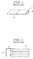
- Figure 1 is a schematic perspective view showing a conventional shield 1.
- Figure 2 is a schematic sectional view showing the dielectric filter 5 equipped with the shield 1.
- the conventional shield 1 is a metal plate shaped like a capital L having a first plate 2 and a second plate 3 perpendicular to the first plate 2.
- the shield 1 is fixed to the dielectric filter 5 by adhering the first plate 2 on the top metallization of the dielectric filter 5.
- the dielectric filter 5 equipped with the shield 1 is mounted on the printed circuit board, the end of the second plate 3 and the ground electrode formed on the printed circuit board are electrically and mechanically connected so that the fluctuation of the potential on the top metallization of the dielectric filter 5 is restrained.
- the end of the second plate 3 of the conventional shield 1 is connected to the ground electrode formed on the printed circuit board, it is necessary that the end of the second plate 3 and the bottom surface of the dielectric filter 5 are coplanar when the shield 1 is attached to the dielectric filter 5.
- the size and the shape of a dielectric block which constitutes the dielectric filter 5 depend on the manufacture conditions, it is extremely difficult to form the shield 1 so that the end of the second plate 3 and the bottom surface of the dielectric filter 5 are coplanar.
- the shield 1 is grounded, the filter characteristics of the dielectric filter 5 changes with the gap between the second plate 3 and the dielectric filter 5.
- the conventional shield 1 is attached to the top metallization of the dielectric filter 5, it is difficult to fix the gap between the second plate 3 and the dielectric filter 5 to a desired distance.
- One of features of the present invention is to provide an improved shield for a dielectric filter that can prevent the thickness of the dielectric filter from increasing without increasing the manufacturing cost of the dielectric filter.
- Another object of the present invention is to provide a dielectric filter equipped with such a shield.
- a shield attachable to a dielectric filter comprising:
- the shield according to the present invention can be attached to the dielectric filter such that the second and third metallic plates pinch the dielectric filter from the side surfaces thereof and that the metallic projecting part is in contact with the metallization of the dielectric filter, the shield does not increase total thickness of the dielectric filter equipped therewith. For this reason, it is enabled to satisfy the demand to thin the total thickness of the dielectric filter. Further, according to the present invention, the distance between the shield and the dielectric filter is fixed by the length of the metallic projecting part. Therefore, the distance does not vary so that the fluctuation of the filter characteristics can be avoided. Moreover, since the shield after attached to the dielectric filter has sufficient mechanical strength, the shield can be made of a thin metal plate.
- a length of the metallic projecting part according to the predetermined direction is shorter than either lengths of the second and third metallic plates according to the predetermined direction.
- the metallic projecting part is elongated from a third end or its adjacent portion, the third end being perpendicular to the first end of the first metallic plate.
- the metallic projecting part is formed on substantially throughout between first and second ends of the first metallic plate.
- the metallic projecting part is formed by folding a part of the first metallic plate using slits formed on the first metallic plate.
- the metallic projecting part is made of projection member attached to the first metallic plate.
- the first metallic plate has a removed portion at a fourth end opposite to the third end.
- the shield further comprises another metallic projecting part elongated from the fourth end or its adjacent portion.
- a shield attachable to a dielectric filter comprising:
- the shield according to the present invention can be attached to the dielectric filter such that the second and third metallic plates pinch the dielectric filter from the side surfaces thereof and that the first and second metallic projecting parts are in contact with the metallization of the dielectric filter, the shield does not increase total thickness of the dielectric filter equipped therewith. Further, according to the present invention, because the distance between the shield and the dielectric filter is fixed by the length of the first and second metallic projecting parts, the distance does not vary so that the fluctuation of the filter characteristics can be avoided. Moreover, since the shield after attached to the dielectric filter has sufficient mechanical strength, the shield can be made of a thin metal plate.
- the first metallic projecting part is formed by folding a part of the second metallic plate using slits formed on the second metallic plate
- the second metallic projecting part is formed by folding a part of the third metallic plate using slits formed on the third metallic plate.
- a dielectric filter comprising:
- the shield because the total thickness of the dielectric filter is not increased by attaching the shield, it is enabled to satisfy the demand to thin the total thickness of the dielectric filter. Further, according to the present invention, because the distance between the shield and the dielectric block is fixed by the length of the metallic projecting part, the distance does not vary so that the fluctuation of the filter characteristics can be avoided. Moreover, since the shield after attached to the dielectric block has sufficient mechanical strength, the shield can be made of a thin metal plate.
- the dielectric filter further comprises a top metallization formed on the top surface of the dielectric block, the top metallization and the third metallization being electrically connected to each other.
- the dielectric block has through holes passing from the third side surface to a fourth side surface opposite to the third surface.
- the metallic projecting part is elongated from a third end or its adjacent portion, the third end being perpendicular to the first end of the first metallic plate.
- the metallic projecting part is formed on substantially throughout between first and second ends of the first metallic plate.
- a fourth end of the first metallic plate opposite to the third end and a bottom surface of the dielectric block opposite to the top surface are substantially coplanar.
- the first metallic plate has a removed portion at the fourth end.
- the dielectric filter further comprises a fourth metallization formed on the third side surface of the dielectric block, the shield further comprising another metallic projection part being in contact with the fourth metallization elongated from the fourth end or its adjacent portion.
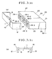
- the shield 10 has a first plate 11, second and third plates 12 and 13 bent substantially perpendicularly to the first plate 11 and a projecting part 14 formed at the upper edge of the first plate 11.
- the shield 10 can be fabricated by bending a piece of metal plate.
- the dielectric block 21 has a top surface 22, a bottom surface 23, side surfaces 24 to 27, and through holes 28-1, 28-2, and 28-3 passing from the side surface 24 to the side surface 25 opposite to the side surface 24. Further, cavities 29-1, 29-2, and 29-3 are formed on the side surface 24 at the portions corresponding to the through holes 28-1, 28-2, and 28-3, respectively.
- a metallization 30-1 is provided on the entire top surface 22, the entire side surfaces 25 to 27, a part of the bottom surface 23 with prevented from contacting with the metallizations 31-1 and 31-2 as input/output terminals by the clearance portions 32, and the inner walls of the through holes 28-1, 28-2, and 28-3 and the cavities 29-1, 29-2, and 29-3; a metallization 30-2 is provided on the upper portion of the side surface 24 of the dielectric block 21.
- the metallizations 30-1 and 30-2 are electrically connected to each other. They are grounded when the dielectric filter 20 is mounted on the printed circuit board.
- the resonators formed by the through holes 28-1, 28-2, and 28-3 are coupled to one another by the cavities 29-1, 29-2, and 29-3 formed on the side surfaces 24 of the dielectric block 21 so that the dielectric filter 20 acts as a band pass filter.
- the metallized portions are shown in the color of the drawing sheet and the portion without metallization is speckled.
- the metallizations 30-1 and 30-2 are formed of silver paste.
- the present invention is not limited to using silver and other kinds of metal can be used instead.
- the distance between the second plate 12 and the third plate 13 of the shield 10 is equal to or a little smaller than the width of the dielectric block 21 (distance between the side surface 26 to the side surface 27). Further, the distance between the lower edge of the first plate 11 and the projecting part 14 of the shield 10 is substantially equal to the distance between the bottom surface 23 of the dielectric block 21 and the metallization 30-2.
- the dielectric filter 20 When attaching the shield 10 to the dielectric filter 20, the dielectric filter 20 should be lied on a planar stage so that the bottom surface 23 faces the stage, and insert the shield 10 such that the second and third plates 12 and 13 pinch the side surfaces 26 and 27 of the dielectric block 21. In this time, the lower edges of the first to third plates 11 to 13 of the shield 10 should be in contact with the stage and the projecting part 14 of the shield 10 should be in contact with the metallization 30-2 of the dielectric filter 20.
- the shield 10 can be attached to the dielectric filter 20 having the width greater than the distance between the second and third plates 12 and 13 since the second and third plates 12 and 13 act as a spring. Therefore, in the case where the shield 10 in which the inside portion 15 and the outside portion 16 of the shield 10 are a little dilated is used, the shield 10 can be surely attached to the dielectric filter 20 even if the width of the dielectric block 21 vary owing to the fabricating conditions.
- a solder metal of high temperature is provided to an interface between the shield 10 and the dielectric filter 20 and reflowing the solder metal to establish the electrical and mechanical connections therebetween. Then, attaching the shield 10 to the dielectric filter 20 is completed.
- Figure 4 is a schematic perspective view from a bottom surface 23 of the dielectric block 21 showing the dielectric filter 20 equipped with the shield 10.
- Figure 5 is a schematic sectional view showing the dielectric filter 20 equipped with the shield 10.
- the lower edge of the shield 10 and the bottom surface 23 of the dielectric block 21 are coplanar. Further, since the distance between the first plate 11 of the shield 10 and the side surface 24 of the dielectric block 21 is fixed by the length of the projecting part 14, the distance does not vary caused by a fluctuation of the fabricating conditions of the dielectric block 21. Moreover, since the projecting part 14 is in contact with the metallization 30-2 provided on the side surface 24 of the dielectric block 21, the total thickness of the dielectric filter 20 does not increase even the shield 10 is attached.
- the metallizations 31-1 and 31-2 as input/output terminals are connected to the signal terminals of the printed circuit board, and the metallization 30-1 provided on the bottom surface 23 of the dielectric block 21 and the lower edge of the first plate 11 of the shield 10 are connected to the ground terminals of the printed circuit board.
- ground potential is applied to the metallization 30-1 provided on the top surface 22 of the dielectric block 21 via not only the metallization 30-1 provided on the side surfaces 25 to 27 of the dielectric block 21 but also the first plate 11 of the shield 10 and the metallization 30-2. Therefore, a fluctuation of the potential on the metallization 30-1 provided on the top surface 22 of the dielectric block 21 is effectively restrained.
- a solder is used to connect the metallizations of the dielectric filter 20 to the electrodes of the printed circuit board.
- the printed circuit board is dipped into a clearing solvent in order to clean a soldering flux off.
- the clearing solvent is provided and discharged to/from the space formed between the shield 10 and the dielectric filter 20 via openings formed by the upper edge of the first plate 11 of the shield 10 except that the projecting part 14 is formed and the dielectric block 21.
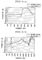
- Figures 6(a) and 6(b) are graphs showing the effect of the shield 10.
- an attenuation in the cut-off band is markedly increased by equipping the dielectric filter 20 with the shield 10.
- the shield 10 of this embodiment is fixed to the dielectric filter 20 by pinching the side surfaces 26 and 27 of the dielectric block 21 and the projecting part 14 is in contact with the metallization 30-2 provided on the side surface 24 of the dielectric block 21. Therefore, a coplanarity of the lower edge of the shield 10 and the bottom surface 23 of the dielectric block 21 can be easily ensured. Further, because the distance between the first plate 11 of the shield 10 and the side surface 24 of the dielectric block 21 is fixed, the distance does not vary so that the fluctuation of the filter characteristics can be avoided. Moreover, since the total thickness of the dielectric filter 20 does not increase even the shield 10 is attached, it is enabled to satisfy the demand to thin.
- the shield 10 is fixed to the dielectric filter 20 by pinching the side surfaces 26 and 27 of the dielectric block 21, a mechanical strength of attached shield 10 is high compared with the conventional shield so that the thin metal plate can be used for the shield 10.
- Figure 7 is a schematic perspective view showing a shield 40 and a dielectric filter 50 to be equipped with the shield 40 that is another preferred embodiment of the present invention.
- the shield 40 has a first plate 41, second and third plate 42 and 43 bent substantially perpendicularly to the first plate 41 and a projecting part 44 formed at the upper edge of the first plate 41.
- the shield 40 has a removed portion 45 formed at the lower edges of the first and second plate 41 and 42 and a removed portion 46 formed at the lower edges of the first and third plates 41 and 43 different from the shield 10 of the above embodiment. Further, the shield 40 of this embodiment is different from the shield 10 that the projecting part 44 is formed on substantially throughout the upper edge of the first plate 41.
- the shield 40 can be fabricated by bending a piece of metal plate. It is preferable that the inside portion and the outside portion of the bent portions of the first and second plates 41 and 42 and the first and third plates 41 and 43 have a little dilated shape.
- the dielectric block 51 has a top surface 52, a bottom surface 53, side surfaces 54 to 57, and through holes 58-1, 58-2, and 58-3 passing from the side surface 54 to the side surface 55 opposite to the side surface 54. No cavities are formed on the side surface 54, that is different from the dielectric filter 20.
- a metallization 60-1 is provided on the entire top surface 52, the entire side surfaces 55 to 57, a part of the bottom surface 53 with prevented from contacting with the metallizations 61-1 and 61-2 as input/output terminals by the clearance portions 62, a part of the side surface 54, and the inner walls of the through holes 58-1, 58-2, and 58-3; a metallization 60-2 is provided on the upper portion of the side surface 54 of the dielectric block 51.
- the metallization 60-1 provided on the side surface 54 has a predetermined pattern.
- the metallizations 60-1 and 60-2 are electrically connected to each other. They are grounded when the dielectric filter 50 is mounted on the printed circuit board.
- Metallizations 63-1 and 63-2 are also provided on the side surface 54 of the dielectric block 51.
- the metallizations 63-1 and 63-2 are connected to the metallizations 61-1 and 61-2 as input/output terminals, respectively.
- the resonators formed by the through holes 58-1, 58-2, and 58-3 are coupled to one another by the metallization 60-1 provided on the side surfaces 54 of the dielectric block 51 so that the dielectric filter 50 acts as a band pass filter.
- the distance between the second plate 42 and the third plate 43 of the shield 40 is equal to or a little smaller than the width of the dielectric block 51 (distance between the side surface 56 to the side surface 57). Further, the distance between the lower edge of the first plate 41 and the projecting part 44 of the shield 40 is substantially equal to the distance between the bottom surface 53 of the dielectric block 51 and the metallization 60-2.
- the same method can be used to attach the shield 40 to the dielectric filter 50 that described above.
- the dielectric filter 50 should be lied on a planar stage so that the bottom surface 53 faces the stage, and inserts the shield 40 such that the second and third plates 42 and 43 pinch the side surfaces 56 and 57 of the dielectric block 51.
- the lower edges of the first to third plates 41 to 43 of the shield 40 should be in contact with the stage and the projecting part 44 of the shield 40 should be in contact with the metallization 60-2 of the dielectric filter 50.
- a solder metal of high temperature is provided to an interface between the shield 40 and the dielectric filter 50 and reflowing the solder metal to establish the electrical and mechanical connections therebetween.
- attaching the shield 40 to the dielectric filter 50 is completed.
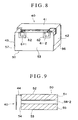
- Figure 8 is a schematic perspective view from a bottom surface 53 of the dielectric block 51 showing the dielectric filter 50 equipped with the shield 40.
- Figure 9 is a schematic sectional view showing the dielectric filter 50 equipped with the shield 40.
- the lower edge of the shield 40 and the bottom surface 53 of the dielectric block 51 are coplanar similar to the above described embodiment. Further, since the distance between the first plate 41 of the shield 40 and the side surface 54 of the dielectric block 51 is fixed by the length of the projecting part 44, the distance does not vary caused by a fluctuation of the fabricating conditions of the dielectric block 51. Moreover, since the projecting part 44 is in contact with the metallization 60-2 provided on the side surface 54 of the dielectric block 51, the total thickness of the dielectric filter 50 does not increase even the shield 40 is attached.
- the metallizations 61-1 and 61-2 as input/output terminals are connected to the signal terminals of the printed circuit board, and the metallization 60-1 provided on the bottom surface 53 of the dielectric block 51 and the lower edge of the first plate 41 of the shield 40 are connected to the ground terminals of the printed circuit board.
- the ground potential is applied to the metallization 60-1 provided on the top surface 52 of the dielectric block 51 via not only the metallization 60-1 provided on the side surfaces 55 to 57 of the dielectric block 51 but also the first plate 41 of the shield 40 and the metallization 60-2. Therefore, a fluctuation of the potential on the metallization 60-1 provided on the top surface 52 of the dielectric block 51 is effectively restrained.
- the shield 40 of this embodiment has the removed portions 45 and 46, the signal wirings elongated from the signal electrodes which are connected to the metallizations 61-1 and 61-2 can be led out through the removed portions 45 and 46. Furthermore, the clearing solvent can be easily provided and discharged to/from the space formed between the shield 40 and the dielectric filter 50 via the removed portions 45 and 46.
- the shield 40 of this embodiment similar effects obtaining by the shield 10 can be also obtained: a coplanarity of the lower edge of the shield 40 and the bottom surface 53 of the dielectric block 51 can be also easily ensured; the distance between the first plate 41 of the shield 40 and the side surface 54 of the dielectric block 51 does not vary; and the total thickness of the dielectric filter 50 does not increase even the shield 40 is attached.
- the shield 40 of this embodiment since the shield 40 of this embodiment has the removed portions 45 and 46, an effect that the signal wirings connected to the metallizations 61-1 and 61-2 can be led out through the removed portions 45 and 46 is obtained.
- Figure 10 is a schematic perspective view showing a shield 70 and a dielectric filter 80 to be equipped with the shield 70 that is a further preferred embodiment of the present invention.
- the shield 70 has a first plate 71, second and third plates 72 and 73 bent substantially perpendicularly to the first plate 71, a first projecting part 74 formed at the upper edge of the first plate 71, and second projecting parts 75-1 and 75-2 elongated from the lower edge of the first plate 71.
- the distance between the first plate 71 and the tip of the first projecting part 74 according to a horizontal direction is substantially the same as the distance between the first plate 71 and the tips of the second projecting parts 75-1 and 75-2 according to a horizontal direction. It is preferable that the inside portion and the outside portion of the bent portions of the first and second plates 71 and 72 and the first and third plates 71 and 73 have a little dilated shape.
- the dielectric filter 80 is a band pass filter, and has the same structure as the dielectric filter 50 except that the metallization 60-3 is provided on the side surface 54 of the dielectric block 51.
- the metallization 60-3 is connected to the metallization 60-1 provided on the bottom surface 53 of the dielectric block 51.
- the distance between the second plate 72 and the third plate 73 of the shield 70 is equal to or a little smaller than the width of the dielectric block 51 (distance between the side surface 56 to the side surface 57). Further, the distance between the tip of the first projecting part 74 and tips of the second projecting parts 75-1 and 75-2 according to a vertical direction is substantially equal to the distance between the metallizations 60-2 and 60-3 provided on the side surface 54 of the dielectric block 51.
- the same method can be used to attach the shield 70 to the dielectric filter 80 that described above.
- the dielectric filter 80 when attaching the shield 70 to the dielectric filter 80, the dielectric filter 80 should be lied on a planar stage so that the bottom surface 53 faces the stage, and inserts the shield 70 such that the second and third plates 72 and 73 pinch the side surfaces 56 and 57 of the dielectric block 51.
- the lower edges of the second and third plates 72 and 73 of the shield 70 should be in contact with the stage
- the first projecting part 74 of the shield 70 should be in contact with the metallization 60-2 of the dielectric filter 80
- the second projecting parts 75-1 and 75-2 of the shield 70 should be in contact with the metallization 60-3 of the dielectric filter 80.
- a solder metal of high temperature is provided to an interface between the shield 70 and the dielectric filter 80 and reflowing the solder metal to establish the electrical and mechanical connections therebetween.
- attaching the shield 70 to the dielectric filter 80 is completed.
- Figure 11 is a schematic perspective view from a bottom surface 53 of the dielectric block 51 showing the dielectric filter 80 equipped with the shield 70.
- Figure 12 is a schematic sectional view showing the dielectric filter 80 equipped with the shield 70.
- the metallizations 61-1 and 61-2 as input/output terminals are connected to the signal terminals of the printed circuit board, and the metallization 60-1 provided on the bottom surface 53 of the dielectric block 51 is connected to the ground terminals of the printed circuit board.
- the ground potential is applied to the metallization 60-1 provided on the top surface 52 of the dielectric block 51 via not only the metallization 60-1 provided on the side surfaces 55 to 57 of the dielectric block 51 but also the metallization 60-3, the first plate 71 of the shield 70 and the metallization 60-2. Therefore, a fluctuation of the potential on the metallization 60-1 provided on the top surface 52 of the dielectric block 51 is effectively restrained.
- the gap is formed between the lower edge of the first plate 71 of the shield 70 and the printed circuit board, the signal wirings elongated from the signal electrodes which are connected to the metallizations 61-1 and 61-2 can be easily led out through the gap. Furthermore, the clearing solvent can be easily provided and discharged to/from the space formed between the shield 70 and the dielectric filter 80 via the gap.
- the shield 70 of this embodiment similar effects obtaining by the shields 10 and 40 can be also obtained: the distance between the first plate 71 of the shield 70 and the side surface 54 of the dielectric block 51 does not vary; and the total thickness of the dielectric filter 80 does not increase even the shield 70 is attached.
- the ground potential is applied to the shield 70 via the metallization 60-3 provided on the side surface 54 of the dielectric block 51, no ground electrode is required to connect to the shield 70. Therefore, a degree of freedom of a design can be increased.
- This embodiment is an example that the shield 40 that is above described embodiment is attached to a dielectric filter consisting of a plurality of resonators each of which is constituted of an individual dielectric block.
- Figure 13 is a schematic perspective view showing a dielectric filter 90 consisting of resonators 91 to 93 and the shield 40 to be attached thereto.
- the dielectric filter 90 to be equipped with the shield 40 consists of three resonators 91 to 93 each of which is constituted of an individual dielectric block. These dielectric blocks have through holes 94 passing from one side surface to the opposite surface and the metallizations provided on the predetermined portions. Coupling between these resonators 91 to 93 is established by exposed portions 95 where no metallization is provided.
- the present invention can be applied to the dielectric filter 90 having aforementioned configuration.
- the dielectric filter 90 is suitable for a custom production because the dielectric filter 90 can be configured by selecting from general resonators (such as the resonators 91 to 93) based on the required characteristics.
- This embodiment is an example that the coupling between the resonators is established by chip components.
- Figure 14 is a schematic perspective view showing a dielectric filter 100 consisting of resonators 101 to 103 and the shield 40 to be attached thereto.
- the dielectric filter 100 to be equipped with the shield 40 consists of three resonators 101 to 103 each of which is constituted of an individual dielectric block. These dielectric blocks have through holes 104 passing from one side surface to the opposite surface and the metallizations provided on the predetermined portions. Coupling between these resonators 101 to 103 is established by chip components 105 mounted thereon.
- the present invention can be applied to the dielectric filter 100 having aforementioned configuration.
- the dielectric filter 100 is suitable for a custom production because the dielectric filter 100 can be configured by selecting from general resonators (such as the resonators 101 to 103) and by selecting from general chip components (such as the components 105) based on the required characteristics.
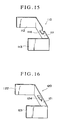
- Figure 15 is a schematic perspective view showing a shield 110 that is a further preferred embodiment of the present invention.
- the shield 110 has a first plate 111, second and third plates 112 and 113 bent substantially perpendicularly to the first plate 111 and a projecting part 114 formed by folding downward the upper portion of the first plate 111 using two parallel slits formed on the first plate 111.
- the shield 110 can be also fabricated by bending a piece of metal plate.
- Figure 16 is a schematic perspective view showing a shield 120 that is a further preferred embodiment of the present invention.
- the shield 120 has a first plate 121, second and third plates 122 and 123 bent substantially perpendicularly to the first plate 121 and a projecting part 124 formed by folding upward the upper portion of the first plate 121 using three slits formed on the first plate 121.
- the shield 120 can be also fabricated by bending a piece of metal plate.
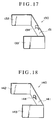
- Figure 17 is a schematic perspective view showing a shield 130 that is a further preferred embodiment of the present invention.
- the shield 130 has a first plate 131, second and third plates 132 and 133 bent substantially perpendicularly to the first plate 131 and a projecting part 134 formed by folding sideways the upper portion of the first plate 131 using two slits perpendicular to each other formed on the first plate 131.
- the shield 130 can be also fabricated by bending a piece of metal plate.
- Figure 18 is a schematic perspective view showing a shield 140 that is a further preferred embodiment of the present invention.
- the shield 140 has a first plate 141, second and third plates 142 and 143 bent substantially perpendicularly to the first plate 141 and a projecting part 144 formed by folding sideways the upper portion of the first plate 141 using three slits formed on the first plate 141.
- the shield 140 can be also fabricated by bending a piece of metal plate.
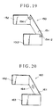
- Figure 19 is a schematic perspective view showing a shield 150 that is a further preferred embodiment of the present invention.
- the shield 150 has a first plate 151, second and third plates 152 and 153 bent substantially perpendicularly to the first plate 151, a first projecting part 154-1 formed by folding downward the upper portion of the second plate 152 using a first slit formed on the edge along the first plate 151 and a second slit parallel to the first slit, and a second projecting part 154-2 formed by folding downward the upper portion of the third plate 153 using a third slit formed on the edge along the first plate 151 and a fourth slit parallel to the third slit.
- the shield 150 can be also fabricated by bending a piece of metal plate.
- Figure 20 is a schematic perspective view showing a shield 160 that is a further preferred embodiment of the present invention.
- the shield 160 has a first plate 161, second and third plates 162 and 163 bent substantially perpendicularly to the first plate 161 and a projecting member 164 adhered to the upper portion of the first plate 161.
- the shield 160 can be fabricated by bending a piece of metal plate and adhering the projecting member 164.
- a ceramic composed mainly of barium titanate is used as the material of the dielectric blocks.
- the present invention is not limited to use of this material and dielectric blocks can instead be made of any of various other materials such as ceramic of barium oxide type.
- the present invention is not limited to use of silver paste and any of various other conductive materials, copper (coppering), for example, can be used instead.
- copper copper
- the copper plating can be performed with a resist formed on the portion where the metallizations should not be formed in advance. It is preferable to use an electroless plating.
- each dielectric filter to be equipped with the shield is the band pass filter
- the present invention is not limited that the dielectric filter to be equipped with the shield is the band pass filter but the shield of the present invention can be attached to other kinds of dielectric filter such as duplexer.
- the shield that can prevent the thickness of a dielectric filter from increasing without increasing the manufacturing cost of the dielectric filter and the dielectric filter equipped therewith can be provided.
Landscapes
- Physics & Mathematics (AREA)
- Electromagnetism (AREA)
- Control Of Motors That Do Not Use Commutators (AREA)
- Shielding Devices Or Components To Electric Or Magnetic Fields (AREA)
Applications Claiming Priority (2)
| Application Number | Priority Date | Filing Date | Title |
|---|---|---|---|
| JP2001097017A JP2002299907A (ja) | 2001-03-29 | 2001-03-29 | シールド板及びこれが装着された誘電体フィルタ |
| JP2001097017 | 2001-03-29 |
Publications (2)
| Publication Number | Publication Date |
|---|---|
| EP1246291A2 true EP1246291A2 (de) | 2002-10-02 |
| EP1246291A3 EP1246291A3 (de) | 2005-01-19 |
Family
ID=18950859
Family Applications (1)
| Application Number | Title | Priority Date | Filing Date |
|---|---|---|---|
| EP02007241A Ceased EP1246291A3 (de) | 2001-03-29 | 2002-03-28 | Abschirmung für dielektrisches Filter und damit versehenes dielektrisches Filter |
Country Status (5)
| Country | Link |
|---|---|
| US (1) | US6734764B2 (de) |
| EP (1) | EP1246291A3 (de) |
| JP (1) | JP2002299907A (de) |
| KR (1) | KR100656563B1 (de) |
| CN (1) | CN1170366C (de) |
Cited By (2)
| Publication number | Priority date | Publication date | Assignee | Title |
|---|---|---|---|---|
| WO2005069426A1 (de) * | 2004-01-13 | 2005-07-28 | Epcos Ag | Duplexer mit schirmung und niedriger bauhöhe |
| GB2555180A (en) * | 2016-07-29 | 2018-04-25 | Radio Design Ltd | Filter apparatus and method of use thereof |
Families Citing this family (2)
| Publication number | Priority date | Publication date | Assignee | Title |
|---|---|---|---|---|
| JP3809817B2 (ja) | 2002-12-19 | 2006-08-16 | 株式会社村田製作所 | 誘電体フィルタ、誘電体デュプレクサおよび通信装置 |
| CN107706488B (zh) * | 2017-09-30 | 2020-12-11 | 厦门松元电子有限公司 | 一种结构型多阶谐振带通滤波器 |
Family Cites Families (20)
| Publication number | Priority date | Publication date | Assignee | Title |
|---|---|---|---|---|
| US4742562A (en) * | 1984-09-27 | 1988-05-03 | Motorola, Inc. | Single-block dual-passband ceramic filter useable with a transceiver |
| US4954796A (en) * | 1986-07-25 | 1990-09-04 | Motorola, Inc. | Multiple resonator dielectric filter |
| JPH0628801Y2 (ja) * | 1987-12-10 | 1994-08-03 | 株式会社村田製作所 | 誘電体フィルタ |
| US5214329A (en) * | 1989-12-07 | 1993-05-25 | Harris Corporation | Bias current modulation for differentially coupled transistor circuit |
| US5144269A (en) * | 1990-03-20 | 1992-09-01 | Sanyo Electric Co., Ltd. | Dielectric filter having external connection formed on dielectric substrate |
| FI87852C (fi) * | 1991-04-12 | 1993-02-25 | Lk Products Oy | Avstaembart keramiskt filter och foerfarande foer dess avstaemning |
| US5130682A (en) * | 1991-04-15 | 1992-07-14 | Motorola, Inc. | Dielectric filter and mounting bracket assembly |
| US5218329A (en) * | 1992-03-25 | 1993-06-08 | Motorola, Inc. | Low profile ceramic filter with self aligning shield |
| US5278527A (en) * | 1992-07-17 | 1994-01-11 | Motorola, Inc. | Dielectric filter and shield therefor |
| JPH07170104A (ja) * | 1993-12-13 | 1995-07-04 | Sony Corp | 誘電体共振器を用いた表面実装部品 |
| JPH07235805A (ja) * | 1994-02-22 | 1995-09-05 | Murata Mfg Co Ltd | 誘電体フィルタ |
| JP3339223B2 (ja) * | 1994-12-26 | 2002-10-28 | 株式会社村田製作所 | 誘電体共振器装置 |
| US5666093A (en) * | 1995-08-11 | 1997-09-09 | D'ostilio; James Phillip | Mechanically tunable ceramic bandpass filter having moveable tabs |
| JP3582922B2 (ja) * | 1995-12-22 | 2004-10-27 | Necトーキン株式会社 | 誘電体フィルタ及びその調整方法 |
| KR970054817A (ko) * | 1995-12-27 | 1997-07-31 | 이형도 | 듀플렉스 유전체 필터 |
| US5745018A (en) | 1996-07-09 | 1998-04-28 | Motorola Inc. | Ceramic filter with a coplanar shield |
| JPH10190313A (ja) * | 1996-12-26 | 1998-07-21 | Kyocera Corp | 表面実装型誘電体フィルタ |
| JP2001053503A (ja) * | 1999-08-13 | 2001-02-23 | Tdk Corp | 誘電体フィルタ |
| KR100343778B1 (ko) * | 1999-12-20 | 2002-07-20 | 한국전자통신연구원 | 전자파 차폐용 차폐물을 갖는 고주파 필터 |
| KR100388017B1 (ko) * | 2000-12-09 | 2003-06-18 | 삼성전기주식회사 | 유전체 블록의 차폐장치 |
-
2001
- 2001-03-29 JP JP2001097017A patent/JP2002299907A/ja active Pending
-
2002
- 2002-03-27 KR KR1020020016711A patent/KR100656563B1/ko not_active Expired - Fee Related
- 2002-03-28 EP EP02007241A patent/EP1246291A3/de not_active Ceased
- 2002-03-28 US US10/112,516 patent/US6734764B2/en not_active Expired - Fee Related
- 2002-03-29 CN CNB021087229A patent/CN1170366C/zh not_active Expired - Fee Related
Cited By (3)
| Publication number | Priority date | Publication date | Assignee | Title |
|---|---|---|---|---|
| WO2005069426A1 (de) * | 2004-01-13 | 2005-07-28 | Epcos Ag | Duplexer mit schirmung und niedriger bauhöhe |
| GB2555180A (en) * | 2016-07-29 | 2018-04-25 | Radio Design Ltd | Filter apparatus and method of use thereof |
| GB2555180B (en) * | 2016-07-29 | 2021-06-09 | Radio Design Ltd | Filter apparatus and method of use thereof |
Also Published As
| Publication number | Publication date |
|---|---|
| EP1246291A3 (de) | 2005-01-19 |
| JP2002299907A (ja) | 2002-10-11 |
| US6734764B2 (en) | 2004-05-11 |
| US20020140528A1 (en) | 2002-10-03 |
| KR100656563B1 (ko) | 2006-12-11 |
| CN1170366C (zh) | 2004-10-06 |
| KR20020077140A (ko) | 2002-10-11 |
| CN1379546A (zh) | 2002-11-13 |
Similar Documents
| Publication | Publication Date | Title |
|---|---|---|
| US5208565A (en) | Dielectric filer having a decoupling aperture between coaxial resonators | |
| US4673902A (en) | Dielectric material coaxial resonator filter directly mountable on a circuit board | |
| EP0859423B1 (de) | Dielektrisches Filter und dielektrischer Duplexer | |
| US5079528A (en) | Dielectric filter | |
| EP0865094A2 (de) | Wellenfilter mit zwei oder mehr dielektrischen Koaxialresonatoren in Juxtaposition | |
| EP1246291A2 (de) | Abschirmung für dielektrisches Filter und damit versehenes dielektrisches Filter | |
| US4737744A (en) | Integrated capacitors for forming components of bandpass filters | |
| JPH02284501A (ja) | 表面実装型ストリップライン共振器 | |
| US20100029241A1 (en) | Rf filter/resonator with protruding tabs | |
| JPH03254201A (ja) | 誘電体帯域阻止フィルタ | |
| US6181223B1 (en) | Dielectric duplexer device | |
| JPH06268464A (ja) | ノイズフィルタブロック | |
| JPH08250962A (ja) | Lcフィルタ | |
| JP2846744B2 (ja) | 誘電体共振器及び誘電体フィルタ | |
| JPS63109601A (ja) | フイルタ | |
| JP4360534B2 (ja) | リード端子、レゾネータ及び電子部品連 | |
| US5939959A (en) | Dielectric filter with elevated inner regions adjacent resonator openings | |
| JP2661004B2 (ja) | 誘電体フィルタ | |
| JPH0212722Y2 (de) | ||
| JPS63299607A (ja) | 面実装形バンドパスフィルタ | |
| KR100199330B1 (ko) | 유전체 필터 | |
| US6034579A (en) | Dielectric filter of the band elimination type | |
| KR200153872Y1 (ko) | 일체형 유전체 필터 | |
| JP2025529413A (ja) | 通信機器用フィルタ | |
| JPH08172302A (ja) | 高誘電率合成樹脂平面フィルタ |
Legal Events
| Date | Code | Title | Description |
|---|---|---|---|
| PUAI | Public reference made under article 153(3) epc to a published international application that has entered the european phase |
Free format text: ORIGINAL CODE: 0009012 |
|
| AK | Designated contracting states |
Kind code of ref document: A2 Designated state(s): AT BE CH CY DE DK ES FI FR GB GR IE IT LI LU MC NL PT SE TR |
|
| AX | Request for extension of the european patent |
Free format text: AL;LT;LV;MK;RO;SI |
|
| RIN1 | Information on inventor provided before grant (corrected) |
Inventor name: TAKUBO, OSAMU Inventor name: ENDO, KENJI |
|
| PUAL | Search report despatched |
Free format text: ORIGINAL CODE: 0009013 |
|
| AK | Designated contracting states |
Kind code of ref document: A3 Designated state(s): AT BE CH CY DE DK ES FI FR GB GR IE IT LI LU MC NL PT SE TR |
|
| AX | Request for extension of the european patent |
Extension state: AL LT LV MK RO SI |
|
| 17P | Request for examination filed |
Effective date: 20050509 |
|
| AKX | Designation fees paid |
Designated state(s): DE FR GB |
|
| STAA | Information on the status of an ep patent application or granted ep patent |
Free format text: STATUS: THE APPLICATION HAS BEEN REFUSED |
|
| 18R | Application refused |
Effective date: 20070429 |