EP1246241A2 - Semiconductor package - Google Patents
Semiconductor package Download PDFInfo
- Publication number
- EP1246241A2 EP1246241A2 EP20020251806 EP02251806A EP1246241A2 EP 1246241 A2 EP1246241 A2 EP 1246241A2 EP 20020251806 EP20020251806 EP 20020251806 EP 02251806 A EP02251806 A EP 02251806A EP 1246241 A2 EP1246241 A2 EP 1246241A2
- Authority
- EP
- European Patent Office
- Prior art keywords
- interposer
- wiring layer
- semiconductor chip
- light blocking
- semiconductor package
- Prior art date
- Legal status (The legal status is an assumption and is not a legal conclusion. Google has not performed a legal analysis and makes no representation as to the accuracy of the status listed.)
- Withdrawn
Links
Images


Classifications
-
- H—ELECTRICITY
- H10—SEMICONDUCTOR DEVICES; ELECTRIC SOLID-STATE DEVICES NOT OTHERWISE PROVIDED FOR
- H10W—GENERIC PACKAGES, INTERCONNECTIONS, CONNECTORS OR OTHER CONSTRUCTIONAL DETAILS OF DEVICES COVERED BY CLASS H10
- H10W42/00—Arrangements for protection of devices
- H10W42/20—Arrangements for protection of devices protecting against electromagnetic or particle radiation, e.g. light, X-rays, gamma-rays or electrons
-
- H—ELECTRICITY
- H10—SEMICONDUCTOR DEVICES; ELECTRIC SOLID-STATE DEVICES NOT OTHERWISE PROVIDED FOR
- H10W—GENERIC PACKAGES, INTERCONNECTIONS, CONNECTORS OR OTHER CONSTRUCTIONAL DETAILS OF DEVICES COVERED BY CLASS H10
- H10W70/00—Package substrates; Interposers; Redistribution layers [RDL]
- H10W70/60—Insulating or insulated package substrates; Interposers; Redistribution layers
- H10W70/62—Insulating or insulated package substrates; Interposers; Redistribution layers characterised by their interconnections
- H10W70/65—Shapes or dispositions of interconnections
- H10W70/657—Shapes or dispositions of interconnections on sidewalls or bottom surfaces of the package substrates, interposers or redistribution layers
-
- H—ELECTRICITY
- H10—SEMICONDUCTOR DEVICES; ELECTRIC SOLID-STATE DEVICES NOT OTHERWISE PROVIDED FOR
- H10W—GENERIC PACKAGES, INTERCONNECTIONS, CONNECTORS OR OTHER CONSTRUCTIONAL DETAILS OF DEVICES COVERED BY CLASS H10
- H10W74/00—Encapsulations, e.g. protective coatings
- H10W74/10—Encapsulations, e.g. protective coatings characterised by their shape or disposition
- H10W74/111—Encapsulations, e.g. protective coatings characterised by their shape or disposition the semiconductor body being completely enclosed
- H10W74/114—Encapsulations, e.g. protective coatings characterised by their shape or disposition the semiconductor body being completely enclosed by a substrate and the encapsulations
-
- H—ELECTRICITY
- H10—SEMICONDUCTOR DEVICES; ELECTRIC SOLID-STATE DEVICES NOT OTHERWISE PROVIDED FOR
- H10W—GENERIC PACKAGES, INTERCONNECTIONS, CONNECTORS OR OTHER CONSTRUCTIONAL DETAILS OF DEVICES COVERED BY CLASS H10
- H10W74/00—Encapsulations, e.g. protective coatings
- H10W74/40—Encapsulations, e.g. protective coatings characterised by their materials
- H10W74/47—Encapsulations, e.g. protective coatings characterised by their materials comprising organic materials, e.g. plastics or resins
- H10W74/473—Encapsulations, e.g. protective coatings characterised by their materials comprising organic materials, e.g. plastics or resins containing a filler
-
- H—ELECTRICITY
- H10—SEMICONDUCTOR DEVICES; ELECTRIC SOLID-STATE DEVICES NOT OTHERWISE PROVIDED FOR
- H10W—GENERIC PACKAGES, INTERCONNECTIONS, CONNECTORS OR OTHER CONSTRUCTIONAL DETAILS OF DEVICES COVERED BY CLASS H10
- H10W70/00—Package substrates; Interposers; Redistribution layers [RDL]
- H10W70/60—Insulating or insulated package substrates; Interposers; Redistribution layers
- H10W70/62—Insulating or insulated package substrates; Interposers; Redistribution layers characterised by their interconnections
- H10W70/65—Shapes or dispositions of interconnections
- H10W70/654—Top-view layouts
- H10W70/655—Fan-out layouts
-
- H—ELECTRICITY
- H10—SEMICONDUCTOR DEVICES; ELECTRIC SOLID-STATE DEVICES NOT OTHERWISE PROVIDED FOR
- H10W—GENERIC PACKAGES, INTERCONNECTIONS, CONNECTORS OR OTHER CONSTRUCTIONAL DETAILS OF DEVICES COVERED BY CLASS H10
- H10W72/00—Interconnections or connectors in packages
- H10W72/071—Connecting or disconnecting
- H10W72/072—Connecting or disconnecting of bump connectors
- H10W72/07251—Connecting or disconnecting of bump connectors characterised by changes in properties of the bump connectors during connecting
-
- H—ELECTRICITY
- H10—SEMICONDUCTOR DEVICES; ELECTRIC SOLID-STATE DEVICES NOT OTHERWISE PROVIDED FOR
- H10W—GENERIC PACKAGES, INTERCONNECTIONS, CONNECTORS OR OTHER CONSTRUCTIONAL DETAILS OF DEVICES COVERED BY CLASS H10
- H10W72/00—Interconnections or connectors in packages
- H10W72/20—Bump connectors, e.g. solder bumps or copper pillars; Dummy bumps; Thermal bumps
-
- H—ELECTRICITY
- H10—SEMICONDUCTOR DEVICES; ELECTRIC SOLID-STATE DEVICES NOT OTHERWISE PROVIDED FOR
- H10W—GENERIC PACKAGES, INTERCONNECTIONS, CONNECTORS OR OTHER CONSTRUCTIONAL DETAILS OF DEVICES COVERED BY CLASS H10
- H10W72/00—Interconnections or connectors in packages
- H10W72/50—Bond wires
- H10W72/531—Shapes of wire connectors
- H10W72/536—Shapes of wire connectors the connected ends being ball-shaped
-
- H—ELECTRICITY
- H10—SEMICONDUCTOR DEVICES; ELECTRIC SOLID-STATE DEVICES NOT OTHERWISE PROVIDED FOR
- H10W—GENERIC PACKAGES, INTERCONNECTIONS, CONNECTORS OR OTHER CONSTRUCTIONAL DETAILS OF DEVICES COVERED BY CLASS H10
- H10W72/00—Interconnections or connectors in packages
- H10W72/50—Bond wires
- H10W72/531—Shapes of wire connectors
- H10W72/5363—Shapes of wire connectors the connected ends being wedge-shaped
-
- H—ELECTRICITY
- H10—SEMICONDUCTOR DEVICES; ELECTRIC SOLID-STATE DEVICES NOT OTHERWISE PROVIDED FOR
- H10W—GENERIC PACKAGES, INTERCONNECTIONS, CONNECTORS OR OTHER CONSTRUCTIONAL DETAILS OF DEVICES COVERED BY CLASS H10
- H10W72/00—Interconnections or connectors in packages
- H10W72/50—Bond wires
- H10W72/541—Dispositions of bond wires
- H10W72/5449—Dispositions of bond wires not being orthogonal to a side surface of the chip, e.g. fan-out arrangements
-
- H—ELECTRICITY
- H10—SEMICONDUCTOR DEVICES; ELECTRIC SOLID-STATE DEVICES NOT OTHERWISE PROVIDED FOR
- H10W—GENERIC PACKAGES, INTERCONNECTIONS, CONNECTORS OR OTHER CONSTRUCTIONAL DETAILS OF DEVICES COVERED BY CLASS H10
- H10W72/00—Interconnections or connectors in packages
- H10W72/50—Bond wires
- H10W72/551—Materials of bond wires
- H10W72/552—Materials of bond wires comprising metals or metalloids, e.g. silver
-
- H—ELECTRICITY
- H10—SEMICONDUCTOR DEVICES; ELECTRIC SOLID-STATE DEVICES NOT OTHERWISE PROVIDED FOR
- H10W—GENERIC PACKAGES, INTERCONNECTIONS, CONNECTORS OR OTHER CONSTRUCTIONAL DETAILS OF DEVICES COVERED BY CLASS H10
- H10W74/00—Encapsulations, e.g. protective coatings
-
- H—ELECTRICITY
- H10—SEMICONDUCTOR DEVICES; ELECTRIC SOLID-STATE DEVICES NOT OTHERWISE PROVIDED FOR
- H10W—GENERIC PACKAGES, INTERCONNECTIONS, CONNECTORS OR OTHER CONSTRUCTIONAL DETAILS OF DEVICES COVERED BY CLASS H10
- H10W74/00—Encapsulations, e.g. protective coatings
- H10W74/01—Manufacture or treatment
- H10W74/012—Manufacture or treatment of encapsulations on active surfaces of flip-chip devices, e.g. forming underfills
-
- H—ELECTRICITY
- H10—SEMICONDUCTOR DEVICES; ELECTRIC SOLID-STATE DEVICES NOT OTHERWISE PROVIDED FOR
- H10W—GENERIC PACKAGES, INTERCONNECTIONS, CONNECTORS OR OTHER CONSTRUCTIONAL DETAILS OF DEVICES COVERED BY CLASS H10
- H10W74/00—Encapsulations, e.g. protective coatings
- H10W74/10—Encapsulations, e.g. protective coatings characterised by their shape or disposition
- H10W74/15—Encapsulations, e.g. protective coatings characterised by their shape or disposition on active surfaces of flip-chip devices, e.g. underfills
-
- H—ELECTRICITY
- H10—SEMICONDUCTOR DEVICES; ELECTRIC SOLID-STATE DEVICES NOT OTHERWISE PROVIDED FOR
- H10W—GENERIC PACKAGES, INTERCONNECTIONS, CONNECTORS OR OTHER CONSTRUCTIONAL DETAILS OF DEVICES COVERED BY CLASS H10
- H10W90/00—Package configurations
- H10W90/701—Package configurations characterised by the relative positions of pads or connectors relative to package parts
- H10W90/721—Package configurations characterised by the relative positions of pads or connectors relative to package parts of bump connectors
- H10W90/724—Package configurations characterised by the relative positions of pads or connectors relative to package parts of bump connectors between a chip and a stacked insulating package substrate, interposer or RDL
Definitions
- the present invention relates to a semiconductor package, and particularly, to a technique of preventing the generation of leak current due to photoexcitation in a thin semiconductor package.
- a earlier semiconductor package is thinned by (1) thinning an interposer of the package and by (2) thinning a resin mold of the package.
- An example of a semiconductor package thinned by the techniques (1) and (2) is a Thin Quad Outline Nonleaded (TQON) package.
- the TQON package employs a flip-chip connection process and guarantees a package thickness of 0.5 mm or thinner.
- Figure 1 is a sectional view showing a semiconductor package according to a related art
- Fig. 2 is a plan view showing a wiring layer formed on an interposer of the package of Fig. 1.
- the wiring layer 48 is formed on the interposer 40.
- a semiconductor chip 10 is mounted upside down and connected to the wiring layer 48 by flip-chip contacts 20.
- the interposer 40, the wiring layer 48, and the contacts 20 are sealed with an underfill material 30.
- the chip 10 and the underfill material 30 are sealed with a resin mold 60.
- the wiring layer 48 includes conductors that are spaced widely apart from one another.
- the thin package according to the related art has a problem (1) that the interposer allows the transmission of light which optically excites semiconductor elements in the semiconductor chip and generates leakage current causing malfunctions.
- the related art fabricates the interposer from a resin substrate made of, for example, glass epoxy resin, Bismaleimide Triazine (BT) resin, or polyimide (PI) resin, instead of a metal lead frame.
- the related art also has a problem (2) that the resin mold on the semiconductor chip allows the transmission of light, in particular, light of 780 nm or longer in wavelength which optically excites the semiconductor elements and generates leakage current causing malfunctions.
- the problem (2) occurs when the resin mold on the semiconductor chip is excessively thinned to reduce the thickness of the package.
- a semiconductor package includes an interposer, a wiring layer formed on the interposer, a semiconductor chip electrically connected to the wiring layer, and a resin mold protecting the wiring layer and semiconductor chip.
- the wiring layer includes conductors formed adjacent to each other at intervals that cause no short circuit among the conductors.
- the package is provided with a light blocking layer formed in areas on the interposer where the conductors are not present.
- the semiconductor package according to the first embodiment includes (a) an interposer 40, (b) a wiring layer 50 containing conductors formed adjacent to each other at intervals that cause no short circuit among the conductors, the wiring layer 50 covering a given area of the interposer 40, to block light from passing through the given area, (c) a light blocking layer 80 covering a no-wiring area of the interposer 40 not covered by the wiring layer 50, to block light from passing through the no-wiring area, (d) a semiconductor chip 10 electrically connected to the wiring layer 50, and (e) a resin mold 62 sealing the wiring layer 50, the light blocking layer 80, and the chip 10.
- An underfill material 30 seals flip-chip contacts 20 that electrically connect the chip 10, which is mounted upside down, to the wiring layer 50.
- the underfill material 30 improves the connection reliability of the contacts 20.
- the resin mold 62 may contain light blocking components such as carbon black powder and metal oxide powder. Even if the resin mold 62 is thinned to about 0.100 mm, the light blocking components in the resin mold 62 allow the transmittance of only about 0 to 1% of light of 780 nm or longer in wavelength.
- the interposer 40 is made of, for example, organic material such as BT resin or PI resin.
- the wiring layer 50 is made of light blocking conductive material such as copper (Cu), aluminum (Al), and copper-nickel (Cu-Ni) alloy.
- the wiring layer 50 electrically connects terminals of chip 10 to external terminals 70.
- the light blocking layer 80 is formed where the wiring layer 50 is not present, for example, under the chip 10 and at the corners of the package.
- the light blocking layer 80 is made of light blocking material which may be conductive or nonconductive. Simultaneously forming the wiring layer 50 and light blocking layer 80 reduces the number of processes. In this regard, it is preferable to simultaneously form the light blocking layer 80 and wiring layer 50 from the same material.
- the conductors in the wiring layer 50 cover a large part of the interposer 40 and are formed adjacent to each other at intervals that cause no short circuit among the conductors.
- the interval between the conductors must be in the range of, for example, 0.010 to 0.100 mm.
- wider intervals are preferred between the conductors. Wider intervals, however, increase the risk of light permeation.
- the light wavelengths that must be blocked vary, and depending on the light wavelengths to be blocked, the adequate interval changes.
- an interval between adjacent conductors in the wiring layer 50 is, for example, about 0.050 mm.
- the light blocking layer 80 consists of a light blocking layer 80a and light blocking layers 80b formed where no wiring layer is present, i.e., under the chip 10 and at the corners of the package.
- the interposer 40 is made of a polyimide tape in this example.
- the semiconductor chip 10 is set in an upside-down configuration, and the wiring layer 50 and chip 10 are connected to each other by the contacts 20.
- the chip 10 and wiring layer 50 are sealed with the resin mold 62, to complete the semiconductor package.
- the semiconductor package according to the first embodiment differs from the related art in that the conductors in the wiring layer 50 are arranged adjacent to each other at intervals that cause no short circuit among the conductors and in that the light blocking layer 80 is added.
- the conductors are arranged adjacent to each other at intervals as close as possible without causing short circuit among the conductors, in order to prevent light from passing through gaps between the conductors.
- the light blocking layer 80 formed in areas where there is no wiring layer prevents light from reaching the semiconductor chip 10 through the no-wiring area.
- the semiconductor package according to the first embodiment differs from the related art in that the resin mold 62 contains light blocking components. Adding light blocking components to the resin mold 62 prevents light from passing through the resin mold 62 even if the resin mold 62 is thin.
- Blocking light from reaching the semiconductor chip 10 prevents semiconductor elements in the chip 10 from being optically excited to generate leakage current, thereby preventing the malfunctions of the elements.
- a resin mold 60 contains no light blocking components. Instead, a light blocking layer 82 is formed on the semiconductor chip 10.
- the light blocking layer 82 is formed by, for example, a spatter deposition method or an electroless plating method, to have a thickness in the range of, for example, 100 to 10000 angstroms.
- the light blocking layer 82 may contain, for example, gold (Au), nickel (Ni), or carbon (C).
- the resin mold 60 according to the second embodiment contains no light blocking components, and therefore, is unable to block light.
- the second embodiment forms the light blocking layer 82 on the chip 10, to block light passing through the resin mold 60 from reaching the chip 10.
- the second embodiment forms a light blocking layer 80 between the chip 10 and an interposer 40, to prevent light passing through the interposer 40 from reaching the chip 10.
- Fig. 6A to 6F are plan views showing various shapes of wiring layers and light blocking layers on interposers in semiconductor packages formed according to the first or second embodiments.
- a numeral 20 is a flip-chip contact
- 50 is a wiring layer
- 70 is an external connection terminal
- 80 is a light blocking layer.
- Fig. 6A two (upper left and upper right) corners among the four corners of the interposer are covered with light blocking layers 80b, and the remaining (lower left and lower right) corners are covered with conductors 50a of the wiring layer 50.
- Fig. 6C the four corners of the interposer are covered with conductors of the wiring layer 50 like Fig. 6B.
- some conductors for example the upper right conductor 50b
- Fig. 6C no conductor is provided with a plurality of flip-chip contacts.
- some conductors of a wiring layer in a semiconductor package according to an embodiment of the present invention may each have two or more contacts connected to a semiconductor chip.
- each side of the interposer is provided with five external connection terminals 70.
- each side of the interposers are provided with seven external connection terminals 70.
- the number of external connection terminals 70 on a side of an interposer according to the present invention is optional and is not limited to 5 or 7.
- external connection terminals 70 are arranged along each edge of each interposer and at intermediate positions between the edges of the interposer and semiconductor chip. More precisely, the external connection terminals 70a are arranged along each edge of each interposer, and the external connection terminals 70b are arranged at intermediate positions between the edges of the interposer and the semiconductor chip.
- an end of a conductor (for example, 50c) at the edge of the semiconductor chip branches into two.
- the semiconductor package according to the third embodiment includes the interposer 40, the wiring layer 54 and the light blocking layer 84 formed on the interposer 40, the semiconductor chip 10, the metal wires 90 electrically connecting the semiconductor chip 10 to the wiring layer 54, and the resin mold 64 protecting the semiconductor chip 10, the wiring layer 54, and the metal wires 90.
- the semiconductor chip 10 is mounted in a face-up position and is connected to the wiring layer 54 by the metal wires 90.
- the light blocking layer 84 under the chip 10 is larger than the chip 10.
- the third embodiment further nesures the prevention of light passing through the interposer 40 from reaching the chip 10. If the light blocking layer 84 is smaller than the chip 10, light passing through gaps between the wiring layer 54 and the light blocking layer 84 may directly contact with the chip 10. According to the third embodiment, the light blocking layer 84 under the chip 10 is larger than the chip 10, and therefore, light passing through gaps between the wiring layer 54 and the light blocking layer 84 never directly reaches the chip 10 because the chip 10 is not present right above the gaps.
- the third embodiment adds light blocking components to the resin mold 64, to block light from passing through the resin mold 64 to the chip 10.
- the semiconductor package according to any one of the embodiments of the present invention minimizes the gaps between conductors of a wiring layer on the interposer of the package and arranges a light blocking layer in areas where the wiring layer is not present, to block light from passing through the interposer, thereby preventing leakage current from being generated by semiconductor elements in the package. This prevents malfunction and reduces power consumption of the package.
Landscapes
- Structures Or Materials For Encapsulating Or Coating Semiconductor Devices Or Solid State Devices (AREA)
- Wire Bonding (AREA)
Abstract
Description
- The present invention relates to a semiconductor package, and particularly, to a technique of preventing the generation of leak current due to photoexcitation in a thin semiconductor package.
- A earlier semiconductor package is thinned by (1) thinning an interposer of the package and by (2) thinning a resin mold of the package. An example of a semiconductor package thinned by the techniques (1) and (2) is a Thin Quad Outline Nonleaded (TQON) package. The TQON package employs a flip-chip connection process and guarantees a package thickness of 0.5 mm or thinner.
- Figure 1 is a sectional view showing a semiconductor package according to a related art, and Fig. 2 is a plan view showing a wiring layer formed on an interposer of the package of Fig. 1.
- In Fig. 1, the
wiring layer 48 is formed on theinterposer 40. Asemiconductor chip 10 is mounted upside down and connected to thewiring layer 48 by flip-chip contacts 20. Theinterposer 40, thewiring layer 48, and thecontacts 20 are sealed with anunderfill material 30. Thechip 10 and theunderfill material 30 are sealed with aresin mold 60. - Under the
chip 10, there are only thecontacts 20 and there is nowiring layer 48. - In Fig. 2, the
wiring layer 48 includes conductors that are spaced widely apart from one another. - The thin package according to the related art has a problem (1) that the interposer allows the transmission of light which optically excites semiconductor elements in the semiconductor chip and generates leakage current causing malfunctions. This is because, in order to thin the interposer, the related art fabricates the interposer from a resin substrate made of, for example, glass epoxy resin, Bismaleimide Triazine (BT) resin, or polyimide (PI) resin, instead of a metal lead frame. The related art also has a problem (2) that the resin mold on the semiconductor chip allows the transmission of light, in particular, light of 780 nm or longer in wavelength which optically excites the semiconductor elements and generates leakage current causing malfunctions. The problem (2) occurs when the resin mold on the semiconductor chip is excessively thinned to reduce the thickness of the package.
- According to an embodiment of the present invention, a semiconductor package includes an interposer, a wiring layer formed on the interposer, a semiconductor chip electrically connected to the wiring layer, and a resin mold protecting the wiring layer and semiconductor chip. The wiring layer includes conductors formed adjacent to each other at intervals that cause no short circuit among the conductors. The package is provided with a light blocking layer formed in areas on the interposer where the conductors are not present.
- Figure 1 is a sectional view showing a semiconductor package according to a related art;
- Fig. 2 is a plan view showing a wiring layer formed on an interposer in the package of Fig. 1;
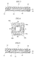
- Fig. 3 is a sectional view showing a semiconductor package according to a first embodiment of the present invention;
- Fig. 4 is a plan view showing a wiring layer and light blocking layer formed on an interposer in the package of Fig. 3;
- Fig. 5 is a sectional view showing a semiconductor package according to a second embodiment of the present invention;
- Figs. 6A to 6F are plan views showing various shapes of wiring layers and light blocking layers on interposers in semiconductor packages formed according to any one of the first and second embodiments;
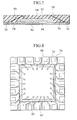
- Fig. 7 is a sectional view showing a semiconductor package according to a third embodiment of the present invention; and
- Fig. 8 is a plan view showing a wiring layer and light blocking layer formed on an interposer, a semiconductor chip, and metal wires in the package of Fig. 7.
-
- Various embodiments of the present invention will be described with reference to the accompanying drawings. It is to be noted that the same or similar reference numerals are applied to the same or similar parts and elements throughout the drawings, and the description of the same or similar parts and elements will be omitted or simplified.
- As shown in Fig.3 and 4, the semiconductor package according to the first embodiment includes (a) an
interposer 40, (b) awiring layer 50 containing conductors formed adjacent to each other at intervals that cause no short circuit among the conductors, thewiring layer 50 covering a given area of theinterposer 40, to block light from passing through the given area, (c) alight blocking layer 80 covering a no-wiring area of theinterposer 40 not covered by thewiring layer 50, to block light from passing through the no-wiring area, (d) asemiconductor chip 10 electrically connected to thewiring layer 50, and (e) aresin mold 62 sealing thewiring layer 50, thelight blocking layer 80, and thechip 10. - An
underfill material 30 seals flip-chip contacts 20 that electrically connect thechip 10, which is mounted upside down, to thewiring layer 50. Theunderfill material 30 improves the connection reliability of thecontacts 20. - The
resin mold 62 may contain light blocking components such as carbon black powder and metal oxide powder. Even if theresin mold 62 is thinned to about 0.100 mm, the light blocking components in theresin mold 62 allow the transmittance of only about 0 to 1% of light of 780 nm or longer in wavelength. - The
interposer 40 is made of, for example, organic material such as BT resin or PI resin. - The
wiring layer 50 is made of light blocking conductive material such as copper (Cu), aluminum (Al), and copper-nickel (Cu-Ni) alloy. Thewiring layer 50 electrically connects terminals ofchip 10 toexternal terminals 70. - The
light blocking layer 80 is formed where thewiring layer 50 is not present, for example, under thechip 10 and at the corners of the package. Thelight blocking layer 80 is made of light blocking material which may be conductive or nonconductive. Simultaneously forming thewiring layer 50 andlight blocking layer 80 reduces the number of processes. In this regard, it is preferable to simultaneously form thelight blocking layer 80 andwiring layer 50 from the same material. - In Fig. 4, the conductors in the
wiring layer 50 cover a large part of theinterposer 40 and are formed adjacent to each other at intervals that cause no short circuit among the conductors. To block natural light from passing through gaps between the conductors, the interval between the conductors must be in the range of, for example, 0.010 to 0.100 mm. To prevent short circuit, wider intervals are preferred between the conductors. Wider intervals, however, increase the risk of light permeation. Depending on the environment of use of semiconductor package according to the embodiment, the light wavelengths that must be blocked vary, and depending on the light wavelengths to be blocked, the adequate interval changes. According to the first embodiment, an interval between adjacent conductors in thewiring layer 50 is, for example, about 0.050 mm. - According to the embodiment, the
light blocking layer 80 consists of alight blocking layer 80a andlight blocking layers 80b formed where no wiring layer is present, i.e., under thechip 10 and at the corners of the package. - A technique of simultaneously forming the
wiring layer 50 andlight blocking layer 80 on theinterposer 40 will be explained. Theinterposer 40 is made of a polyimide tape in this example. - (1) A thin copper film is entirely formed on the surface of the polyimide tape where the wiring layer, etc., are formed.
- (2) A photoresist layer is entirely formed on the thin copper film.
- (3) A mask to form the wiring layer and light blocking layer is set on
the photoresist layer and is exposed to light such as ultraviolet rays, electron
beams, or ion beams.
The photoresist layer may be made of a resin that melts when exposed
to light. In this case, the mask is shaped to be identical with the
wiring layer 50 andlight blocking layers - (4) A developer is applied to remove unnecessary parts from the photoresist layer. If the photoresist layer is made of resin that melts by exposure, the patterns left on the photoresist layer after the development coincide with the shape of the mask. If the photoresist layer is made of resin that hardens by exposure, the patterns left on the photoresist layer after the development coincide with a negative-positive inverted shape of the mask.
- (5) An etching process is carried out to remove copper at parts not protected by the photoresist layer. As a result, only the parts of the copper thin film protected by the photoresist layer remain on the polyimide tape.
- (6) The photoresist layer is removed, to leave the
wiring layer 50 andlight blocking layer 80 on the polyimide tape. -
- On the
wiring layer 50, thesemiconductor chip 10 is set in an upside-down configuration, and thewiring layer 50 andchip 10 are connected to each other by thecontacts 20. Thechip 10 andwiring layer 50 are sealed with theresin mold 62, to complete the semiconductor package. - As explained above, the semiconductor package according to the first embodiment differs from the related art in that the conductors in the
wiring layer 50 are arranged adjacent to each other at intervals that cause no short circuit among the conductors and in that thelight blocking layer 80 is added. The conductors are arranged adjacent to each other at intervals as close as possible without causing short circuit among the conductors, in order to prevent light from passing through gaps between the conductors. Thelight blocking layer 80 formed in areas where there is no wiring layer prevents light from reaching thesemiconductor chip 10 through the no-wiring area. - The semiconductor package according to the first embodiment differs from the related art in that the
resin mold 62 contains light blocking components. Adding light blocking components to theresin mold 62 prevents light from passing through theresin mold 62 even if theresin mold 62 is thin. - Blocking light from reaching the
semiconductor chip 10 prevents semiconductor elements in thechip 10 from being optically excited to generate leakage current, thereby preventing the malfunctions of the elements. - Only a differences in the second embodiment from the first embodiment will be explained. According to the semiconductor package of the second embodiment as shown in Fig.5, a
resin mold 60 contains no light blocking components. Instead, alight blocking layer 82 is formed on thesemiconductor chip 10. - The
light blocking layer 82 is formed by, for example, a spatter deposition method or an electroless plating method, to have a thickness in the range of, for example, 100 to 10000 angstroms. Thelight blocking layer 82 may contain, for example, gold (Au), nickel (Ni), or carbon (C). - The
resin mold 60 according to the second embodiment contains no light blocking components, and therefore, is unable to block light. To cope with this, the second embodiment forms thelight blocking layer 82 on thechip 10, to block light passing through theresin mold 60 from reaching thechip 10. - Like the first embodiment, the second embodiment forms a
light blocking layer 80 between thechip 10 and aninterposer 40, to prevent light passing through theinterposer 40 from reaching thechip 10. - Fig. 6A to 6F are plan views showing various shapes of wiring layers and light blocking layers on interposers in semiconductor packages formed according to the first or second embodiments. In Figs. 6A to 6F, a numeral 20 is a flip-chip contact, 50 is a wiring layer, 70 is an external connection terminal, and 80 is a light blocking layer.
- In Fig. 6A, two (upper left and upper right) corners among the four corners of the interposer are covered with light blocking layers 80b, and the remaining (lower left and lower right) corners are covered with
conductors 50a of thewiring layer 50. - In Fig. 6B, the four corners of the interposer are covered with
conductors 50b of thewiring layer 50. - In Fig. 6C, the four corners of the interposer are covered with conductors of the
wiring layer 50 like Fig. 6B. In Fig. 6B, some conductors (for example the upperright conductor 50b) are provided with a plurality of flip-chip contacts (20a, 20b). In Fig. 6C, no conductor is provided with a plurality of flip-chip contacts. In this way, some conductors of a wiring layer in a semiconductor package according to an embodiment of the present invention may each have two or more contacts connected to a semiconductor chip. - In Fig. 6D, each side of the interposer is provided with five
external connection terminals 70. In Figs. 6A to 6C, each side of the interposers are provided with sevenexternal connection terminals 70. The number ofexternal connection terminals 70 on a side of an interposer according to the present invention is optional and is not limited to 5 or 7. - In Figs. 6E and 6F,
external connection terminals 70 are arranged along each edge of each interposer and at intermediate positions between the edges of the interposer and semiconductor chip. More precisely, theexternal connection terminals 70a are arranged along each edge of each interposer, and theexternal connection terminals 70b are arranged at intermediate positions between the edges of the interposer and the semiconductor chip. - In Fig. 6F, an end of a conductor (for example, 50c) at the edge of the semiconductor chip branches into two.
- As shown in Figs.7 and 8, the semiconductor package according to the third embodiment includes the
interposer 40, thewiring layer 54 and thelight blocking layer 84 formed on theinterposer 40, thesemiconductor chip 10, themetal wires 90 electrically connecting thesemiconductor chip 10 to thewiring layer 54, and theresin mold 64 protecting thesemiconductor chip 10, thewiring layer 54, and themetal wires 90. - Only differences in the third embodiment from the first embodiment will be explained. According to the third embodiment, the
semiconductor chip 10 is mounted in a face-up position and is connected to thewiring layer 54 by themetal wires 90. - The
light blocking layer 84 under thechip 10 is larger than thechip 10. - Compared with the first embodiment, the third embodiment further nesures the prevention of light passing through the
interposer 40 from reaching thechip 10. If thelight blocking layer 84 is smaller than thechip 10, light passing through gaps between thewiring layer 54 and thelight blocking layer 84 may directly contact with thechip 10. According to the third embodiment, thelight blocking layer 84 under thechip 10 is larger than thechip 10, and therefore, light passing through gaps between thewiring layer 54 and thelight blocking layer 84 never directly reaches thechip 10 because thechip 10 is not present right above the gaps. - As in the first embodiment, the third embodiment adds light blocking components to the
resin mold 64, to block light from passing through theresin mold 64 to thechip 10. - As explained above, the semiconductor package according to any one of the embodiments of the present invention minimizes the gaps between conductors of a wiring layer on the interposer of the package and arranges a light blocking layer in areas where the wiring layer is not present, to block light from passing through the interposer, thereby preventing leakage current from being generated by semiconductor elements in the package. This prevents malfunction and reduces power consumption of the package.
Claims (13)
- A semiconductor package comprising:an interposer;a wiring layer having a plurality of conductors;a semiconductor chip electrically connected to the wiring layer;a light blocking layer formed between the interposer and the semiconductor chip; anda resin mold sealing the wiring layer, the light blocking layer, and the semiconductor chip.
- A semiconductor package according to claim 1, wherein the wiring layer having a plurality of conductors formed adjacent to each other at intervals that cause no short circuit among the conductors, the wiring layer covering a given area of the interposer, to block light from passing through the given area.
- A semiconductor package according to either of claims 1 or 2, wherein the light blocking layer covering a no-wiring area of the interposer not covered by the wiring layer, to block light passing from through the no-wiring area.
- A semiconductor package according to any of claims 1 to 3, the wiring layer and the light blocking layer are made of the same materials.
- A semiconductor package according to any of claims 1 to 4, wherein an interval between the conductors is in a range of about 0.010 mm to 0.100 mm.
- A semiconductor package according to any of claims 1 to 5, wherein the light blocking layer is formed under the semiconductor chip and at least, at one of the comers of the interposer.
- A semiconductor package according to any of claims 1 to 6, wherein the resin mold contains at least one of carbon black powder and metal oxide powder.
- A semiconductor package according to any of claims 1 to 7, wherein:the semiconductor chip is mounted in a face-down configuration on the interposer; anda light blocking layer is formed on a face of the semiconductor chip opposite to the interposer.
- A semiconductor package according to any of claims 1 to 7, wherein:the semiconductor chip is mounted in a face-up configuration on the interposer; andthe light blocking layer under the semiconductor chip is larger than the semiconductor chip.
- A semiconductor package according to any of claims 1 to 9, wherein contacts between the semiconductor chip and the wiring layer are sealed by an underfill material.
- A semiconductor package according to any of claims 1 to 10, wherein the interposer includes external connection terminals connected to the conductors of the wiring layer, the external connection terminals being arranged along the edge of the interposer and/or at intermediate positions between the edges of the interposer and semiconductor chip.
- A semiconductor package according to any of claims 1 to 11, wherein at least one of the conductors of the wiring layer has at least two contacts in the vicinity of the semiconductor chip, these contacts being usable to connect the conductor to the semiconductor chip.
- A semiconductor package according to any of claims 1 to 11, wherein at least one of the conductors of the wiring layer has an end branched into at least two sections, in the vicinity of the semiconductor chip.
Applications Claiming Priority (2)
| Application Number | Priority Date | Filing Date | Title |
|---|---|---|---|
| JP2001102061A JP4212255B2 (en) | 2001-03-30 | 2001-03-30 | Semiconductor package |
| JP2001102061 | 2001-03-30 |
Publications (2)
| Publication Number | Publication Date |
|---|---|
| EP1246241A2 true EP1246241A2 (en) | 2002-10-02 |
| EP1246241A3 EP1246241A3 (en) | 2005-05-18 |
Family
ID=18955305
Family Applications (1)
| Application Number | Title | Priority Date | Filing Date |
|---|---|---|---|
| EP20020251806 Withdrawn EP1246241A3 (en) | 2001-03-30 | 2002-03-13 | Semiconductor package |
Country Status (6)
| Country | Link |
|---|---|
| US (1) | US7148529B2 (en) |
| EP (1) | EP1246241A3 (en) |
| JP (1) | JP4212255B2 (en) |
| KR (1) | KR100731332B1 (en) |
| CN (1) | CN1210791C (en) |
| TW (1) | TW538485B (en) |
Cited By (1)
| Publication number | Priority date | Publication date | Assignee | Title |
|---|---|---|---|---|
| CN112151507A (en) * | 2019-06-28 | 2020-12-29 | 半导体元件工业有限责任公司 | Anti-glare semiconductor package and related methods |
Families Citing this family (10)
| Publication number | Priority date | Publication date | Assignee | Title |
|---|---|---|---|---|
| KR100541654B1 (en) * | 2003-12-02 | 2006-01-12 | 삼성전자주식회사 | Wiring board and semiconductor device for solid-state imaging using same |
| DE102004057485B4 (en) * | 2004-11-29 | 2007-10-18 | Infineon Technologies Ag | Power semiconductor component and method for its production |
| WO2008081696A1 (en) * | 2006-12-28 | 2008-07-10 | Nichia Corporation | Light emitting device, package, light emitting device manufacturing method, package manufacturing method and package manufacturing die |
| US20080239684A1 (en) * | 2007-04-02 | 2008-10-02 | Shinko Electric Industries Co., Ltd. | Wiring board and method of manufacturing the same |
| US8252634B2 (en) * | 2009-06-19 | 2012-08-28 | Stats Chippac Ltd. | Integrated circuit packaging system with a leadframe having radial-segments and method of manufacture thereof |
| JP2012069734A (en) * | 2010-09-24 | 2012-04-05 | Toshiba Corp | Manufacturing method of semiconductor device |
| JP7238277B2 (en) * | 2018-06-14 | 2023-03-14 | 富士電機株式会社 | Semiconductor device, lead frame and method for manufacturing semiconductor device |
| US11152288B2 (en) * | 2019-04-25 | 2021-10-19 | Infineon Technologies Ag | Lead frames for semiconductor packages |
| JP2022071925A (en) * | 2020-10-29 | 2022-05-17 | ローム株式会社 | Semiconductor device and method for manufacturing semiconductor device |
| CN119069450A (en) * | 2024-11-04 | 2024-12-03 | 杭州暖芯迦电子科技有限公司 | Device for continuous blood glucose monitoring and method of manufacturing the same |
Citations (2)
| Publication number | Priority date | Publication date | Assignee | Title |
|---|---|---|---|---|
| EP0874401A2 (en) * | 1997-04-22 | 1998-10-28 | Nec Corporation | Semiconductor device having a protective wiring layer |
| EP1087440A2 (en) * | 1999-09-22 | 2001-03-28 | Texas Instruments Incorporated | Modeling technique to increase device reliability |
Family Cites Families (36)
| Publication number | Priority date | Publication date | Assignee | Title |
|---|---|---|---|---|
| JPS5568694A (en) * | 1978-11-17 | 1980-05-23 | Matsushita Electric Industrial Co Ltd | Method of forming image on copper |
| US4388128A (en) * | 1980-03-17 | 1983-06-14 | Matsushita Electric Industrial Co., Ltd. | Solid-state color-image sensor and process for fabricating the same |
| JPS58127338A (en) * | 1982-01-25 | 1983-07-29 | Sharp Corp | Structure of electronic part |
| JPS58134449A (en) * | 1982-02-04 | 1983-08-10 | Sharp Corp | Lsi package |
| JPS61112322A (en) * | 1984-11-07 | 1986-05-30 | Nec Corp | Axial aligning method of pattern |
| JPS61174763A (en) * | 1985-01-30 | 1986-08-06 | Hitachi Ltd | solid state imaging device |
| JPS63306633A (en) * | 1987-06-08 | 1988-12-14 | Toshiba Corp | Film carrier |
| JPH01128534A (en) * | 1987-11-13 | 1989-05-22 | Matsushita Electric Ind Co Ltd | Mounting method for semiconductor element on transparent substrate |
| JPH0310224A (en) * | 1989-06-07 | 1991-01-17 | Sharp Corp | Display device |
| JPH0521655A (en) | 1990-11-28 | 1993-01-29 | Mitsubishi Electric Corp | Semiconductor device and package for semiconductor device |
| JPH0824193B2 (en) | 1990-10-16 | 1996-03-06 | 工業技術院長 | Manufacturing method of semiconductor device for driving flat plate type light valve |
| JPH0590549A (en) | 1991-09-27 | 1993-04-09 | Sanyo Electric Co Ltd | Solid-state image sensing element and manufacture thereof |
| JPH0629568A (en) | 1992-07-07 | 1994-02-04 | Nec Corp | Optical coupling element |
| JPH0677526A (en) * | 1992-08-25 | 1994-03-18 | Nippondenso Co Ltd | Resin-sealed photoelectric conversion device and manufacturing method thereof |
| JPH06112371A (en) | 1992-09-30 | 1994-04-22 | Hitachi Ltd | Equipment equipped with an IC chip |
| JPH06132423A (en) | 1992-10-19 | 1994-05-13 | Sharp Corp | Method for manufacturing semiconductor device |
| JP3206839B2 (en) * | 1992-10-30 | 2001-09-10 | 株式会社シチズン電子 | IC card module structure |
| JP3383398B2 (en) * | 1994-03-22 | 2003-03-04 | 株式会社東芝 | Semiconductor package |
| US5436203A (en) * | 1994-07-05 | 1995-07-25 | Motorola, Inc. | Shielded liquid encapsulated semiconductor device and method for making the same |
| US5625224A (en) * | 1994-08-10 | 1997-04-29 | Motorola, Inc. | Method and apparatus for an integrated circuit chip carrier having improved mounting pad density |
| KR970006014B1 (en) | 1994-09-13 | 1997-04-23 | 현대전자산업 주식회사 | Interface circuit using sector mode algorithms |
| KR100299390B1 (en) * | 1995-06-16 | 2001-10-27 | 가나이 쓰도무 | Liquid crystal display device suitable for narrow frame |
| JPH09307111A (en) | 1996-05-10 | 1997-11-28 | Sony Corp | Semiconductor device |
| US6270193B1 (en) * | 1996-06-05 | 2001-08-07 | Brother Kogyo Kabushiki Kaisha | Ink-jet and ink jet recording apparatus having IC chip attached to head body by resin material |
| US5898217A (en) * | 1998-01-05 | 1999-04-27 | Motorola, Inc. | Semiconductor device including a substrate having clustered interconnects |
| JP3481444B2 (en) * | 1998-01-14 | 2003-12-22 | シャープ株式会社 | Semiconductor device and manufacturing method thereof |
| JP3092575B2 (en) * | 1998-01-20 | 2000-09-25 | 日本電気株式会社 | Resin-sealed semiconductor device |
| JPH11297903A (en) * | 1998-04-07 | 1999-10-29 | Seiko Epson Corp | Semiconductor device |
| JP2000294894A (en) * | 1998-12-21 | 2000-10-20 | Seiko Epson Corp | Circuit board, method of manufacturing the same, and display device and electronic apparatus using the circuit board |
| JP2000277641A (en) | 1999-03-24 | 2000-10-06 | Kyocera Corp | Method for manufacturing optical semiconductor element storage package |
| JP3483798B2 (en) * | 1999-06-16 | 2004-01-06 | シャープ株式会社 | Semiconductor device |
| US6249044B1 (en) * | 1999-06-17 | 2001-06-19 | National Semiconductor Corp. | Opaque metallization to cover flip chip die surface for light sensitive semiconductor devices |
| US6281027B1 (en) * | 1999-09-15 | 2001-08-28 | Therma-Wave Inc | Spatial averaging technique for ellipsometry and reflectometry |
| JP3494948B2 (en) * | 2000-03-22 | 2004-02-09 | シャープ株式会社 | Solid-state imaging device and method of manufacturing the same |
| US6784409B2 (en) * | 2000-03-28 | 2004-08-31 | Canon Kabushiki Kaisha | Electronic device with encapsulant of photo-set resin and production process of same |
| JP3866058B2 (en) * | 2001-07-05 | 2007-01-10 | シャープ株式会社 | Semiconductor device, wiring board and tape carrier |
-
2001
- 2001-03-30 JP JP2001102061A patent/JP4212255B2/en not_active Expired - Fee Related
-
2002
- 2002-03-13 EP EP20020251806 patent/EP1246241A3/en not_active Withdrawn
- 2002-03-19 TW TW91105150A patent/TW538485B/en not_active IP Right Cessation
- 2002-03-20 US US10/101,108 patent/US7148529B2/en not_active Expired - Fee Related
- 2002-03-28 KR KR20020017070A patent/KR100731332B1/en not_active Expired - Fee Related
- 2002-03-29 CN CNB02108727XA patent/CN1210791C/en not_active Expired - Fee Related
Patent Citations (2)
| Publication number | Priority date | Publication date | Assignee | Title |
|---|---|---|---|---|
| EP0874401A2 (en) * | 1997-04-22 | 1998-10-28 | Nec Corporation | Semiconductor device having a protective wiring layer |
| EP1087440A2 (en) * | 1999-09-22 | 2001-03-28 | Texas Instruments Incorporated | Modeling technique to increase device reliability |
Cited By (1)
| Publication number | Priority date | Publication date | Assignee | Title |
|---|---|---|---|---|
| CN112151507A (en) * | 2019-06-28 | 2020-12-29 | 半导体元件工业有限责任公司 | Anti-glare semiconductor package and related methods |
Also Published As
| Publication number | Publication date |
|---|---|
| US7148529B2 (en) | 2006-12-12 |
| JP2002299498A (en) | 2002-10-11 |
| CN1379467A (en) | 2002-11-13 |
| CN1210791C (en) | 2005-07-13 |
| KR20020077198A (en) | 2002-10-11 |
| TW538485B (en) | 2003-06-21 |
| EP1246241A3 (en) | 2005-05-18 |
| JP4212255B2 (en) | 2009-01-21 |
| KR100731332B1 (en) | 2007-06-21 |
| US20020140062A1 (en) | 2002-10-03 |
Similar Documents
| Publication | Publication Date | Title |
|---|---|---|
| US10211114B2 (en) | Microelectronic devices, stacked microelectronic devices, and methods for manufacturing such devices | |
| US6649941B2 (en) | Method for manufacturing semiconductor device using group III nitride compound | |
| US5847458A (en) | Semiconductor package and device having heads coupled with insulating material | |
| KR100540243B1 (en) | Semiconductor device and method for fabricating the same | |
| US20070164457A1 (en) | Semiconductor package, substrate with conductive post, stacked type semiconductor device, manufacturing method of semiconductor package and manufacturing method of stacked type semiconductor device | |
| US20130241020A1 (en) | Solid image-pickup device with flexible circuit substrate | |
| US20090256249A1 (en) | Stacked, interconnected semiconductor package | |
| US20070210437A1 (en) | Semiconductor device and manufacturing method thereof | |
| US7633133B2 (en) | Semiconductor device and manufacturing method of the same | |
| US20240203901A1 (en) | Semiconductor device and method of producing the same | |
| US7148529B2 (en) | Semiconductor package | |
| US8129272B2 (en) | Hidden plating traces | |
| US7806731B2 (en) | Rounded contact fingers on substrate/PCB for crack prevention | |
| US7745907B2 (en) | Semiconductor package including connector disposed in troughhole | |
| US20060097377A1 (en) | Flip chip bonding structure using non-conductive adhesive and related fabrication method | |
| US20050051895A1 (en) | BGA package having semiconductor chip with edge-bonding metal patterns formed thereon and method of manufacturing the same | |
| US20240371846A1 (en) | Optoelectronic device and method for manufacture | |
| KR100556351B1 (en) | Metal pad and metal pad bonding method of semiconductor device | |
| US6936495B1 (en) | Method of making an optoelectronic semiconductor package device | |
| KR20000076811A (en) | Semiconductor device and manufacturing method therefor | |
| CN119108355A (en) | Electronic packaging module and manufacturing method thereof | |
| JP2005039116A (en) | Semiconductor device and method for manufacturing the same | |
| KR20090088265A (en) | Semiconductor package and manufacturing method thereof | |
| KR20060128377A (en) | Multi-chip package |
Legal Events
| Date | Code | Title | Description |
|---|---|---|---|
| PUAI | Public reference made under article 153(3) epc to a published international application that has entered the european phase |
Free format text: ORIGINAL CODE: 0009012 |
|
| 17P | Request for examination filed |
Effective date: 20020325 |
|
| AK | Designated contracting states |
Kind code of ref document: A2 Designated state(s): AT BE CH CY DE DK ES FI FR GB GR IE IT LI LU MC NL PT SE TR |
|
| AX | Request for extension of the european patent |
Free format text: AL;LT;LV;MK;RO;SI |
|
| PUAL | Search report despatched |
Free format text: ORIGINAL CODE: 0009013 |
|
| AK | Designated contracting states |
Kind code of ref document: A3 Designated state(s): AT BE CH CY DE DK ES FI FR GB GR IE IT LI LU MC NL PT SE TR |
|
| AX | Request for extension of the european patent |
Extension state: AL LT LV MK RO SI |
|
| AKX | Designation fees paid |
Designated state(s): DE FR GB |
|
| 17Q | First examination report despatched |
Effective date: 20060524 |
|
| GRAP | Despatch of communication of intention to grant a patent |
Free format text: ORIGINAL CODE: EPIDOSNIGR1 |
|
| RIC1 | Information provided on ipc code assigned before grant |
Ipc: H01L 23/29 20060101ALI20160726BHEP Ipc: H01L 23/498 20060101ALI20160726BHEP Ipc: H01L 23/31 20060101AFI20160726BHEP Ipc: H01L 23/552 20060101ALI20160726BHEP |
|
| INTG | Intention to grant announced |
Effective date: 20160825 |
|
| STAA | Information on the status of an ep patent application or granted ep patent |
Free format text: STATUS: GRANT OF PATENT IS INTENDED |
|
| STAA | Information on the status of an ep patent application or granted ep patent |
Free format text: STATUS: THE APPLICATION IS DEEMED TO BE WITHDRAWN |
|
| 18D | Application deemed to be withdrawn |
Effective date: 20170105 |