EP1243947A2 - Beugungsoptische Komponente, Beleuchtungssystem und Belichtungssytem und -verfahren - Google Patents
Beugungsoptische Komponente, Beleuchtungssystem und Belichtungssytem und -verfahren Download PDFInfo
- Publication number
- EP1243947A2 EP1243947A2 EP02006299A EP02006299A EP1243947A2 EP 1243947 A2 EP1243947 A2 EP 1243947A2 EP 02006299 A EP02006299 A EP 02006299A EP 02006299 A EP02006299 A EP 02006299A EP 1243947 A2 EP1243947 A2 EP 1243947A2
- Authority
- EP
- European Patent Office
- Prior art keywords
- surface wave
- radiation
- substrate
- waves
- surface waves
- Prior art date
- Legal status (The legal status is an assumption and is not a legal conclusion. Google has not performed a legal analysis and makes no representation as to the accuracy of the status listed.)
- Granted
Links
- 230000003287 optical effect Effects 0.000 title claims abstract description 72
- 238000005286 illumination Methods 0.000 title claims description 6
- 238000000034 method Methods 0.000 title description 5
- 230000003993 interaction Effects 0.000 claims abstract description 126
- 230000005855 radiation Effects 0.000 claims abstract description 111
- 239000000758 substrate Substances 0.000 claims abstract description 111
- 238000005259 measurement Methods 0.000 claims abstract description 22
- 238000010897 surface acoustic wave method Methods 0.000 claims abstract description 18
- 238000003384 imaging method Methods 0.000 claims description 12
- 230000005284 excitation Effects 0.000 claims description 7
- 230000008878 coupling Effects 0.000 claims description 6
- 238000010168 coupling process Methods 0.000 claims description 6
- 238000005859 coupling reaction Methods 0.000 claims description 6
- 238000004519 manufacturing process Methods 0.000 claims description 6
- 230000005469 synchrotron radiation Effects 0.000 claims description 6
- 230000001360 synchronised effect Effects 0.000 claims description 4
- 238000013016 damping Methods 0.000 claims description 3
- 230000007423 decrease Effects 0.000 claims description 3
- 238000001208 nuclear magnetic resonance pulse sequence Methods 0.000 claims 1
- 230000008859 change Effects 0.000 description 8
- 239000000463 material Substances 0.000 description 8
- 230000006870 function Effects 0.000 description 7
- 230000010363 phase shift Effects 0.000 description 7
- 238000013461 design Methods 0.000 description 6
- 230000001419 dependent effect Effects 0.000 description 5
- 230000008901 benefit Effects 0.000 description 4
- 239000002245 particle Substances 0.000 description 4
- 238000001228 spectrum Methods 0.000 description 4
- 230000000694 effects Effects 0.000 description 3
- 230000000737 periodic effect Effects 0.000 description 3
- 229910052782 aluminium Inorganic materials 0.000 description 2
- XAGFODPZIPBFFR-UHFFFAOYSA-N aluminium Chemical compound [Al] XAGFODPZIPBFFR-UHFFFAOYSA-N 0.000 description 2
- 238000010276 construction Methods 0.000 description 2
- GQYHUHYESMUTHG-UHFFFAOYSA-N lithium niobate Chemical compound [Li+].[O-][Nb](=O)=O GQYHUHYESMUTHG-UHFFFAOYSA-N 0.000 description 2
- 238000001459 lithography Methods 0.000 description 2
- 230000008569 process Effects 0.000 description 2
- 238000012545 processing Methods 0.000 description 2
- WSMQKESQZFQMFW-UHFFFAOYSA-N 5-methyl-pyrazole-3-carboxylic acid Chemical compound CC1=CC(C(O)=O)=NN1 WSMQKESQZFQMFW-UHFFFAOYSA-N 0.000 description 1
- 229910017119 AlPO Inorganic materials 0.000 description 1
- JBRZTFJDHDCESZ-UHFFFAOYSA-N AsGa Chemical compound [As]#[Ga] JBRZTFJDHDCESZ-UHFFFAOYSA-N 0.000 description 1
- OKTJSMMVPCPJKN-UHFFFAOYSA-N Carbon Chemical compound [C] OKTJSMMVPCPJKN-UHFFFAOYSA-N 0.000 description 1
- RYGMFSIKBFXOCR-UHFFFAOYSA-N Copper Chemical compound [Cu] RYGMFSIKBFXOCR-UHFFFAOYSA-N 0.000 description 1
- -1 Li 2 B 4 O 7 ) Chemical compound 0.000 description 1
- 229910013641 LiNbO 3 Inorganic materials 0.000 description 1
- VYPSYNLAJGMNEJ-UHFFFAOYSA-N Silicium dioxide Chemical compound O=[Si]=O VYPSYNLAJGMNEJ-UHFFFAOYSA-N 0.000 description 1
- 230000004913 activation Effects 0.000 description 1
- ILRRQNADMUWWFW-UHFFFAOYSA-K aluminium phosphate Chemical compound O1[Al]2OP1(=O)O2 ILRRQNADMUWWFW-UHFFFAOYSA-K 0.000 description 1
- HGECAQBPRPOUAG-UHFFFAOYSA-N bismuth;oxogermanium Chemical class [Bi].[Ge]=O HGECAQBPRPOUAG-UHFFFAOYSA-N 0.000 description 1
- 238000004364 calculation method Methods 0.000 description 1
- 238000001816 cooling Methods 0.000 description 1
- 229910052802 copper Inorganic materials 0.000 description 1
- 239000010949 copper Substances 0.000 description 1
- 239000013078 crystal Substances 0.000 description 1
- 238000000151 deposition Methods 0.000 description 1
- 239000013013 elastic material Substances 0.000 description 1
- 239000013536 elastomeric material Substances 0.000 description 1
- 238000005516 engineering process Methods 0.000 description 1
- 238000005530 etching Methods 0.000 description 1
- 238000007667 floating Methods 0.000 description 1
- MORCTKJOZRLKHC-UHFFFAOYSA-N lithium;oxoboron Chemical class [Li].O=[B] MORCTKJOZRLKHC-UHFFFAOYSA-N 0.000 description 1
- 238000013507 mapping Methods 0.000 description 1
- 229910052751 metal Inorganic materials 0.000 description 1
- 239000002184 metal Substances 0.000 description 1
- 238000001465 metallisation Methods 0.000 description 1
- 150000002739 metals Chemical class 0.000 description 1
- 230000005012 migration Effects 0.000 description 1
- 238000013508 migration Methods 0.000 description 1
- 230000001902 propagating effect Effects 0.000 description 1
- 230000009467 reduction Effects 0.000 description 1
- 239000004065 semiconductor Substances 0.000 description 1
- 230000035945 sensitivity Effects 0.000 description 1
- 238000007493 shaping process Methods 0.000 description 1
- 239000007787 solid Substances 0.000 description 1
- 238000003860 storage Methods 0.000 description 1
- 230000008961 swelling Effects 0.000 description 1
- 230000002123 temporal effect Effects 0.000 description 1
- 230000008646 thermal stress Effects 0.000 description 1
- 238000012549 training Methods 0.000 description 1
Images


Classifications
-
- G—PHYSICS
- G03—PHOTOGRAPHY; CINEMATOGRAPHY; ANALOGOUS TECHNIQUES USING WAVES OTHER THAN OPTICAL WAVES; ELECTROGRAPHY; HOLOGRAPHY
- G03F—PHOTOMECHANICAL PRODUCTION OF TEXTURED OR PATTERNED SURFACES, e.g. FOR PRINTING, FOR PROCESSING OF SEMICONDUCTOR DEVICES; MATERIALS THEREFOR; ORIGINALS THEREFOR; APPARATUS SPECIALLY ADAPTED THEREFOR
- G03F7/00—Photomechanical, e.g. photolithographic, production of textured or patterned surfaces, e.g. printing surfaces; Materials therefor, e.g. comprising photoresists; Apparatus specially adapted therefor
- G03F7/70—Microphotolithographic exposure; Apparatus therefor
- G03F7/70058—Mask illumination systems
- G03F7/7015—Details of optical elements
- G03F7/70158—Diffractive optical elements
-
- G—PHYSICS
- G02—OPTICS
- G02B—OPTICAL ELEMENTS, SYSTEMS OR APPARATUS
- G02B5/00—Optical elements other than lenses
- G02B5/18—Diffraction gratings
-
- G—PHYSICS
- G02—OPTICS
- G02F—OPTICAL DEVICES OR ARRANGEMENTS FOR THE CONTROL OF LIGHT BY MODIFICATION OF THE OPTICAL PROPERTIES OF THE MEDIA OF THE ELEMENTS INVOLVED THEREIN; NON-LINEAR OPTICS; FREQUENCY-CHANGING OF LIGHT; OPTICAL LOGIC ELEMENTS; OPTICAL ANALOGUE/DIGITAL CONVERTERS
- G02F1/00—Devices or arrangements for the control of the intensity, colour, phase, polarisation or direction of light arriving from an independent light source, e.g. switching, gating or modulating; Non-linear optics
- G02F1/29—Devices or arrangements for the control of the intensity, colour, phase, polarisation or direction of light arriving from an independent light source, e.g. switching, gating or modulating; Non-linear optics for the control of the position or the direction of light beams, i.e. deflection
- G02F1/33—Acousto-optical deflection devices
-
- G—PHYSICS
- G03—PHOTOGRAPHY; CINEMATOGRAPHY; ANALOGOUS TECHNIQUES USING WAVES OTHER THAN OPTICAL WAVES; ELECTROGRAPHY; HOLOGRAPHY
- G03F—PHOTOMECHANICAL PRODUCTION OF TEXTURED OR PATTERNED SURFACES, e.g. FOR PRINTING, FOR PROCESSING OF SEMICONDUCTOR DEVICES; MATERIALS THEREFOR; ORIGINALS THEREFOR; APPARATUS SPECIALLY ADAPTED THEREFOR
- G03F7/00—Photomechanical, e.g. photolithographic, production of textured or patterned surfaces, e.g. printing surfaces; Materials therefor, e.g. comprising photoresists; Apparatus specially adapted therefor
- G03F7/70—Microphotolithographic exposure; Apparatus therefor
- G03F7/70216—Mask projection systems
- G03F7/70316—Details of optical elements, e.g. of Bragg reflectors, extreme ultraviolet [EUV] multilayer or bilayer mirrors or diffractive optical elements
Definitions
- the invention relates to an optical diffraction component for Provision of a radiation diffractive grating structure, the lattice structure for diffraction and deflection of a incident light beam by surface waves on a Surface of a substrate can be provided.
- One wavelength of the light to be diffracted at the grating structure first any wavelength from the optical spectrum his.
- the invention relates to one Diffractive optical component for providing a grating structure for diffraction of light in the areas of the ultraviolet, of extreme ultraviolet (EUV), with wavelengths of about 0.1nm to about 100nm, as well as the X-ray range.
- EUV extreme ultraviolet
- the invention further relates to a lighting system which is a light beam, especially from the wavelength ranges Ultraviolet, extreme ultraviolet and x-ray, is distractible and controllable.
- the invention further relates to an exposure system for imaging a provided on a mask Patterns on a substrate, one for illustration used light beam through the diffraction optical Component is controllable and the pattern in particular Components of a miniaturized device.
- the invention further relates to an exposure method for Production of a miniaturized component with one photolithographic step.
- miniaturized components in particular of semiconductor devices, is traditionally a photolithographic step used to get on a Mask predetermined structures onto one with a radiation sensitive Imaging layered substrate and thereby to expose the radiation sensitive layer.
- a lower one Limit of dimensions of the structures shown (CD, "critical dimension") is due to the wavelength of the for given the image used light.
- Components With always smaller structures of the miniaturized to be manufactured Components are therefore always shorter wavelengths of the Use light for illustration.
- wavelengths below ultraviolet imaging optical components and components for beam guidance or deflection are difficult to handle or technologies for such components not yet sufficiently developed. Examples of lighting optics in the The range of the EUV are from US 5 973 826, 6 033 079 and US 6 142 641 known.
- an optical diffraction Component for providing a radiation diffractive
- the invention provides a diffractive optical component a radiation diffractive lattice structure with a high Propose diffraction efficiency at short optical wavelengths.
- Another object of the invention is an exposure system to propose which is comparatively the figure small pattern.
- Another object of the invention is a method to propose for the manufacture of a component which especially for the production of components with small Structures is suitable.
- the invention is based on an optical diffraction component to provide a radiation diffractive grating structure, which comprises a surface acoustic wave device assembly comprising a Substrate, a surface wave source for generating Surface waves on a surface of the substrate and has an interaction area of the substrate surface, for an interaction of the radiation with a lattice structure is provided, which is generated by the surface waves is provided.
- a radiation diffractive grating structure which comprises a surface acoustic wave device assembly comprising a Substrate, a surface wave source for generating Surface waves on a surface of the substrate and has an interaction area of the substrate surface, for an interaction of the radiation with a lattice structure is provided, which is generated by the surface waves is provided.
- the invention lies in a first aspect of the knowledge based on the fact that the SAW lattice structure then has a high Diffraction efficiency can be provided if the SAW grating structure a high quality diffraction grating generated, which ideally by wave trains of surface waves is formed, whose profiles in the entire interaction area same, preferably essentially sinusoidal or have a sinusoidal shape.
- the surface wave source the conventional diffractive optical component in addition to surface waves, which emits towards the interaction area are also emitted surface waves that are not to the Interaction area are directed. This actually from surface waves directed away from the interaction area are reflected at the edges of the substrate and eventually reach the Interaction area where they get the profiles of the directly from the Surface wave source towards the interaction area emitted surface waves and ultimately interfere lower the quality of the optical grating.
- the invention is the idea underlying surface waves that are not towards the interaction area be emitted, not at all on the substrate to generate first.
- the invention proposes as a surface wave source a unidirectional source, i.e. a surface source with a directional characteristic to provide which surface waves emits more in a preferred direction than in one opposite direction, and the surface wave source relative to the interaction area like this to arrange that the surface waves emitted in the preferred direction the interaction area, if necessary also after distraction by means of surface wave mirrors or similar, go through.
- a unidirectional source i.e. a surface source with a directional characteristic to provide which surface waves emits more in a preferred direction than in one opposite direction
- the surface wave source relative to the interaction area like this to arrange that the surface waves emitted in the preferred direction the interaction area, if necessary also after distraction by means of surface wave mirrors or similar, go through.
- the idea lies in a further aspect of the invention underlying that with a view to controlling and changing the Deflection or diffraction angle between incoming and outgoing Beam a lattice constant of the lattice structure must be changeable.
- This is the conventional diffraction optical Component, however, only to a very limited extent in the Location.
- the invention is accordingly based on the idea in which Surface wave assembly a surface wave source use, which contribute to the emission of surface waves designed several different wavelengths is.
- the invention is characterized in that that the surface wave source is an electroacoustic Transducer having an electrode structure comprising a plurality of sub-electrodes that are spaced from neighboring ones Sub-electrodes are arranged.
- the Electrode structure provided a plurality of areas which are side by side in the emission direction of the surface waves and are spaced from each other and wherein in the partial electrodes are arranged periodically in each of the regions are. The different areas differ in that the arrangement periods of the partial electrodes different from each other in the respective areas are.
- the arrangement period of sub-electrodes of one area specifies the wavelength at which this area is surface waves is emitted with increased efficiency by providing of the areas with different arrangement periods created a total surface wave source, which in a comparatively broad wavelength range Emit surface waves with relatively high efficiency can.
- the invention is based on the idea from that to achieve high diffraction efficiency Surface wave grating with high surface wave amplitude is to be provided.
- a surface source with electro-acoustic Transducers can change the amplitude of the surface waves emitted be increased by the fact that electrodes of electroacoustic transducer AC voltages with higher Voltage amplitude can be applied.
- electroacoustic transducer maximum applicable voltage amplitude in practice by electrical flashovers limits between electrodes and partial electrodes of the transducer set.
- the invention is based on the idea to use an electroacoustic transducer, which at Applying a comparatively low voltage already Surface waves generated with high amplitude.
- the invention is characterized by that the electroacoustic transducer has two groups of finger electrodes has, the finger electrodes of each Group electrically connected and the finger electrodes different groups electrically from each other are isolated.
- the electrical drive AC voltage in the operation of the electroacoustic Transducer Between pairs of finger electrodes different groups is at least one of the finger electrodes of the two groups each electrically insulated intermediate electrode provided.
- the electrical potential this intermediate electrode is preferably free adjusting (floating) so that over the components finger electrode the first group, intermediate electrode and finger electrode the other group a voltage divider is provided, in which one between two adjacent Electrode voltage is lower is as the total between the groups of finger electrodes applied voltage. This measure will Tendency to flashover between electrodes of the electroacoustic Converter effectively reduced, although from that electro-acoustic transducer surface waves of high amplitude can be emitted.
- the intermediate electrode as well as the Finger electrodes, a periodic structure, whereby of the intermediate electrode branch electrodes, which are extend between adjacent finger electrodes.
- finger electrodes and branch electrodes it is in terms of the effect of Overall electrode structure as a voltage divider advantageous that the finger electrodes of different groups to each other offset in parallel, but preferably not on one extend common straight lines. It is also here advantageous if finger electrodes and branch electrodes are each other are assigned in pairs and are assigned to each other Branch or finger electrodes are roughly common Straight lines.
- the invention is again the Understanding that to achieve high diffraction efficiency a high amplitude of the radiation diffractive Surface waves providing lattice structure necessary is.
- the invention is based on the idea of a Set the frequency to excite the surface wave source so that the amplitude of that from the surface source emitted surface waves is essentially maximum.
- the invention is characterized by that on the substrate a surface wave receiver for from surface waves emitted by the surface wave source is provided, which provides a measurement signal, which a Represents the amplitude of the surface waves on the Hit surface wave receiver. Then it is still one Control provided which the frequency to excite the Surface wave source depending on the measurement signal of the Surface wave receiver sets.
- This provides an arrangement that allows the frequency to excite the surface wave source so long, if necessary iteratively, to change until the amplitude of the received surface waves essentially maximum is. It can then be assumed that the Surface wave source Surface waves with maximum amplitude emitted and that then also the lattice structure maximum in the interaction area by surface waves Amplitude is provided.
- One with regard to the emission of surface waves surface wave source designed as high as possible typically shows depending on the excitation frequency a course of the amplitude of the emitted surface waves such that at a central frequency Amplitude of the generated surface waves is maximum and the amplitude with a characteristic on both sides of the central frequency Frequency width decreases. Also typically shows a surface wave receiver with the same Amplitude of the received surface waves depending a course of the measurement signal from the surface wave frequency on, which is also on both sides of a central frequency of a characteristic frequency range.
- the surface wave sources and the surface wave receiver are preferably so coordinated that the characteristic frequency range of the surface wave source is smaller than the typical frequency range of the surface wave receiver.
- This interpretation is particularly from the point of view advantageous that the center frequency at the surface wave source due to temperature drifts, for example does not have to be constant over time or the surface wave source to change the deflection or diffraction angle is controlled with changing frequencies. It is then possible to use the frequency to excite the surface wave source depending on the measurement signal alone of the surface acoustic wave receiver to set substantially to achieve the maximum possible surface wave amplitude.
- the invention again proceeds from this from that to achieve a high diffraction efficiency Lattice structure with high lattice quality is necessary.
- this aspect is the basis of the invention, that surface waves coming from the surface wave source were emitted after passing through the interaction area continue to propagate on the substrate until finally meet and from a substrate edge, if necessary via detours, back into the interaction area are reflected and there the profiles of the actually desired Disrupt grid structure.
- the invention proposes surface waves after passing through the interaction area to dampen a surface wave damper so that an intensity to reflect back into the interaction area Surface waves is as low as possible.
- Such a surface wave damper can, for example elastomeric material formed on the substrate is applied and in which the mechanical energy of Surface waves are dissipated in thermal energy.
- a surface wave damper is that that it generates heat on the substrate, causing a change the propagation properties of surface waves on the Leads substrate.
- the surface wave damper as acoustoelectric converter is designed to the mechanical Surface wave energy at the location of the surface wave damper convert into electrical energy.
- the electrical Energy can then in particular without thermal stress of the substrate is transported away from it and on from that Substrate distant site dissipated in a suitable manner be so that a thermal load on the substrate the surface wave damper is comparatively low.
- the acoustoelectric converter preferably has at least two electrical connections on which the generated electrical energy can be tapped by a resistor circuit is connected to the tapped electrical energy in the resistance circuit to dissipate.
- the structures of the electroacoustic transducer are preferred the surface wave source and the acoustoelectric Transducer of the surface wave damper symmetrical to each other, in particular with a symmetrical design of Partial electrodes, formed.
- the invention provides different operating temperatures of surface wave source and surface wave receiver to take into account that order periods of partial electrodes of the electroacoustic transducer Surface wave source and the acoustoelectric converter of the surface wave damper are different from each other, the difference in the order periods on the differences in the expected operating temperatures of the components are coordinated.
- the surface wave damper preferably has a directional characteristic in that he has surface waves that from a preferred direction on the surface wave damper are dampened more than surface waves, which from an opposite direction to the surface wave damper to meet.
- the advantage of such unidirectionality of the surface wave damper can be understood if you take into account that an acoustoelectric Basically, transducers and an electroacoustic transducer can have the same or similar electrode structures.
- a unidirectional electro-acoustic transducer emits surface waves with increased efficiency in a preferred direction from.
- the surface wave damper is preferably arranged in such a way that surface waves that the interaction area have passed through and acted as an optical grating there, are damped by the surface wave damper to to reduce a thermal load on the substrate and around also to avoid these surface waves after Reflection around the edges of the substrate back into the interaction area reach.
- the surface wave damper is preferred also used to absorb surface waves which from the surface wave source not towards that Interaction area are emitted.
- the invention goes again assume that to achieve the highest possible diffraction efficiency high surface wave amplitudes are also necessary are.
- the idea lies in this aspect of the invention underlying surface waves, the interaction area have passed through, not in a surface wave damper to annihilate, but this again the interaction area supply.
- the invention is characterized in that that on the substrate a plurality of mirrors for surface waves is arranged so that the mirror is closed Provide a propagation path for the surface waves and the interaction area in this closed Path of propagation lies. It becomes surface wave energy after passing through the interaction area via the closed path of propagation back into the interaction area returned to an increase in there Contribute surface wave amplitude.
- the surface wave source is preferably also located in the closed propagation path, whereby however the surface wave source has a directional characteristic and Surface waves emitted more strongly in a preferred direction than in an opposite direction.
- the preferred direction the surface wave source thereby defines the direction of rotation the surface waves in the closed propagation path firmly.
- This Training has the advantage that the surface wave source not even the highest amplitude of surface waves is exposed and thus the surface wave source has a comparatively longer service life as effects such as Material migration in the structures of the surface wave source are reduced.
- the coupling of those emitted by the surface wave source is preferably carried out by means of a mirror that the surface waves to be coupled into the closed propagation path reflected and that for surface waves that Propagate along the closed path of propagation, transparent is.
- the invention is again the Thought based on that to achieve high diffraction efficiency to advantageously use a grating with high grating amplitudes is.
- the invention is characterized by that the radiation diffractive grating structure in the interaction area standing surface waves on the substrate is provided. This can be done, for example achieved that on the substrate by means of surface wave mirrors or other deflecting elements for surface waves a surface wave resonator is built, i.e. a Structure in which surface waves resonate can, and thus an increase in amplitude in the resonator revolving waves can be achieved.
- the surface waves covering the interaction area have passed through one or more mirrors again in the essentially in phase in the interaction area be reflected back, especially the paths of propagation of surface waves immediately after their Pass through the interaction area and after reflection can collapse back to the interaction area and only differ in their direction.
- the surface wave source outside the resonator and thus outside the Path of propagation of the surface waves arranged in the resonator and that is from the surface wave source outside of the resonator emitted surface waves in the Resonator are coupled. This has the advantage that the Surface wave source itself not the high surface wave amplitudes exposed in the resonator what to longer life of the surface wave source.
- the coupling of the surface waves into the resonator surface wave source arranged outside the resonator is preferably carried out via a surface wave mirror.
- the diffraction optical explained above Component with one provided by surface waves
- Lattice structure used in a lighting system which in addition to the diffraction optical component, there is also a radiation source includes whose radiation on the interaction area the surface acoustic wave assembly is directed.
- the radiation of the radiation source falling on the interaction region is bent or deflected at the lattice structure, wherein by changing an operation of the surface acoustic wave device the lattice structure is changeable and so that the diffraction angle or deflection angle can be specifically changed.
- a radiation source is a radiation source of any kind to understand what their radiation is immediately or indirectly, i.e. after one or more reflections or with the interposition of imaging optical elements etc., aimed at the interaction area.
- a radiation source is a radiation source of any kind to understand what their radiation is immediately or indirectly, i.e. after one or more reflections or with the interposition of imaging optical elements etc., aimed at the interaction area.
- virtual radiation sources which are visible for the interaction area and whose light falls on the interaction area.
- the radiation source emits on the interaction area directed radiation preferably continuously what especially in versions where the surface waves propagate continuously in the interaction area, can be exploited to have a deflected beam to produce constant intensity.
- the radiation source of the lighting system is a pulsed one Radiation source, i.e. a radiation source, which their Radiation is not emitted with a constant intensity over time. It is then further provided that the radiation source with the the standing surface wave generating surface wave assembly to synchronize so that at times or in periods when the radiation source emitted intensity a comparatively high value also has the amplitudes of the standing surface waves have a comparatively high value. This means, that the radiation pulses are always on the lattice structure meet if this is also their essentially maximum Has lattice amplitude.
- a continuous source of radiation with a time-varying closure for example a chopper wheel, is combined, and an intrinsically pulsed radiation source, such as a pulse train emitting laser or also a synchrotron, whose charged particles as particle packets circulate in the storage ring.
- an intrinsically pulsed radiation source such as a pulse train emitting laser or also a synchrotron, whose charged particles as particle packets circulate in the storage ring.
- a controller provided by means of which a frequency and a phase position of the generated surface waves is adjustable, the control device responsive to a signal which is the pulse train the radiation source or a sequence of partial pulses Radiation source represents. It will then be through the Control the times at which the generated lattice structure has large lattice amplitudes, adapted to the times, where also the intensity of the radiation source emitted radiation is high.
- a controller that controls the frequency and phasing of the pulses emitted by the radiation source to the amplitudes adjust the grid structure.
- the Radiation source in relation to the surface acoustic wave assembly synchronized.
- An advantageous application of the lighting system is in the exposure of a substrate with patterns or images, i.e. with a location-dependent radiation intensity.
- a substrate preferably provided by a mask
- the lighting system is supplemented by an imaging system, which maps the mask onto the substrate.
- the exposure system thus formed preferably comprises a substrate holder and a mask holder, to which one to exposing substrate or a pattern to be imaged default mask are attachable such that their effective Areas in a predetermined substrate level or mask level of the lighting system are arranged.
- a Condenser provided the light of the radiation source, which on the lattice structure in different spatial directions was bent, focusing on the mask.
- Radiation can be radiation at a time for example in different diffraction orders, i.e. different diffraction angles, has been bent, and it can are also radiation that coincide in time different deflection or diffraction angle deflected has been. This can happen, for example, that a Lattice period of the lattice structure is changed over time, by the surface wave construction arrangement with time different frequencies is excited.
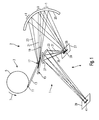
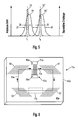
- FIG. 1 shows schematically an embodiment of an inventive Exposure system 1, which is an illumination system 2 and an imaging system 4.
- the lighting system 1 comprises a radiation source 3 in the form of a 1 schematically represented as a ring 5 synchrotrons, in which electrons revolve in the direction of an arrow 7 and emit synchrotron radiation.
- the beam feed can be direct or indirect for example deflecting mirrors, focusing components, wavelength selective components, etc.
- On the Diffractive optical component 15 is an interaction area 17 provided on the at least part of the beam 13 is directed so that from the point of view of the interaction area 17 the radiation striking it directly from a Source or an equivalent virtual source to come seems.
- wavelength-selective components such as Bragg monochromators or the like can cover all possible wavelength ranges the synchrotron radiation and the interaction area 17 are supplied.
- this is Radiation with a radiation wavelength of 0.1nm to 100nm, preferably 1nm to 50nm and in this case special Wavelengths around 13nm.
- the interaction region 17 There is a lattice structure in the interaction region 17 provided which is a reflection grating for the incident Radiation 13 represents.
- the incident radiation 13 reflects and thereby Grating diffraction split into three partial beams 19, 21 and 23, namely the ray 21 0 order, the ray 23 +1. Order and the beam 19 -1.
- Order Here is the divergence of the diffracted beams 19, 23 by the frequency spectrum of the incident beam 13 is determined because of the diffraction angle for a given grating period from the wavelength of the diffracted Light is dependent.
- the partial beams 19, 21 and 23 meet one focusing acting condenser mirror 25, which reflects the partial beams and aimed at the surface of a mask 27.
- the of the condenser 25 partial beams directed onto the mask 27 19, 21, 23 illuminate a common area lighting spot 29.
- Mask 27 is a reflection mask, the structure shown in FIG. 1 as straight line 28 at which the incident radiation 19, 21, 23 reflects becomes.
- the rays 19, 21, 23 illuminates which from three different spatial directions meet the mask 27. Accordingly, the rays 19, 21, 23 also by the structure specified on the mask 27 28 in three different spatial directions as rays 31, 33, 35 reflected.
- the reflected rays are from the Imaging system 4 recorded and imaged on a substrate 39.
- the imaging system 4 comprises a lens mirror 37, which rays 31, 33, 35 hit, and the latter on the substrate 39 such that the structures of the Mask 27 are imaged on the substrate 39.
- Figure 1 is accordingly the line structure 28 on the mask 27 on the Mapped substrate 39 by radiation only in the Area of a line segment 41 falls onto the substrate 39.
- the illumination system 1 is an imaging one System created that the mask 27 on the substrate 39th images, the mask 27 from several spatial directions is exposed even though the beam originating from the source 11 13 is highly collimated. It is based on that of the incident beam 13 with a given collinearity a lighting system with a comparatively high numerical Aperture realized, or in other words, the diffraction optical Component 15 has to increase the light conductance of the Lighting system contributed.
- the lattice structure can be adjusted by changing the lattice period, about the diffraction angles of beams 19 and 23 of-1. or +1. Change order. It is therefore possible to Angles at which the rays 19, 23 fall on the mask 27, also vary in time, so that within one Time a solid angle range for illuminating the mask 27 can be essentially completely illuminated.
- the lighting system 1 can be used, for example, in a method for producing a miniaturized component and there in particular in a photolithographic Methods section.
- the substrate in which the Component to be manufactured in advance with a radiation sensitive Layer coated.
- On the radiation sensitive Layer is then with the lighting system 1 of Figure 1 projected the pattern of the mask 27.
- the radiation sensitive Layer developed, and subsequently performed one or more processing steps that the Change substrate in certain areas, depending on the situation whether the area is an area with developed or not developed photosensitive layer.
- etching steps or doping steps, etc. into consideration.
- the lighting system 1 is shown in FIG. 1 as a simplified one System shown in functional representation. So there exist Condenser and the lens each from a mirror 25 or 37. However, it is possible to make the components more complex design and other beam-shaping in the beam path and inserting beam deflecting components. Such components and their use in a lithography system for example from US 5 973 826, US 6 033 079 and 6 142 641 known, these writings by reference in full be included in the present application.
- Illumination system 1 An essential component of that shown in Figure 1 Illumination system 1 is the diffraction optical component 15, on the interaction area 17 of the incident and to be deflected Beam 13 falls.
- This diffraction optical component is shown in more detail in Figure 2.
- This comprises a substrate 43 with a substrate surface 45 on which surface waves can be excited with high amplitude efficiency. Under The term surface waves are all wave phenomena here in the substrate matter to understand which one periodic change in the optical properties of the Guide substrate surface 45.
- SAW surface acoustic waves
- Surface waves polarized perpendicular to the surface of the substrate as well as surface waves polarized parallel to the surface, such as Bleustein-Gulyaev waves can be. It is also possible to superposition such Use waves.
- SAWs surface acoustic waves
- the substrate 43 is made from a single crystal of lithium niobate (LiNbO 3 ) in such a way that the substrate surface 45 forms a 128 ° rotY surface.
- the material lithium niobate was selected as the substrate material because it is a piezoelectric material and piezoelectric materials are particularly suitable for the excitation of surface waves by electrical voltages or fields in a surface wave source 47.
- there are also other suitable piezoelectric materials as substrates 43 such as lithium tantalate (LiTaO 3 ), quartz (SiO 2 ), lithium boron oxides (e.g.
- Li 2 B 4 O 7 aluminum phosphate (AlPO 4 ), gallium arsenide (GaAs ), Polybismuthites, especially bismuth germanium oxides (eg Bi 12 GeO 20 or Bi 12 SiO 20 ) and others.
- AlPO 4 aluminum phosphate
- GaAs gallium arsenide
- Polybismuthites especially bismuth germanium oxides (eg Bi 12 GeO 20 or Bi 12 SiO 20 ) and others.
- the surface wave source 47 comprises an electro-acoustic one Transducer 51, which is used to generate the surface waves required energy as electrical energy at connections 49 and 50 is supplied.
- the electroacoustic transducer 51 is a unidirectional transducer, which means that it has surface waves that converge into one Spread out by arrow 53, with generates a much higher intensity than surface waves, which is in an opposite direction to 53 Spread towards 54.
- the electroacoustic transducer 51 comprises a partial transducer 55 which is optimized with regard to the generation of surface waves with a wavelength ⁇ 1 of 30 ⁇ m, and a partial transducer 57 which is optimized with regard to the generation of surface waves with a wavelength ⁇ 2 of 20 ⁇ m is optimized.
- a partial transducer 57 which is optimized with regard to the generation of surface waves with a wavelength ⁇ 2 of 20 ⁇ m is optimized.
- wavelengths ⁇ in the range from approximately 2 ⁇ m to 100 ⁇ m, in particular 4 ⁇ m to 50 ⁇ m, with excitation frequencies from 50 MHz to 2 GHz are provided.
- FIG. 5 shows with curves 52 and 52 'a frequency characteristic of the electroacoustic transducer 51.
- curve 52 represents the surface wave intensity emitted by sub-transducer 55 as a function of the electrical excitation frequency of the transducer
- curve 52' correspondingly for sub-transducer 57 represents.
- the two partial transducers 55, 57 generate surface waves at different frequencies f 1 and f 2 with maximum intensity.
- the transducer 51 comprises a plurality of sets of finger electrodes, So-called interdigital electrodes, as shown in FIG. 4 becomes clear, which magnifies an area in which the partial transducers 55 and 57 of FIG. 3 adjoin one another.
- the converter 51 comprises a collecting electrode 59 on which the electrical connection 49 is provided and which is in the emission direction 53 extends.
- Another collecting electrode 60 extends parallel to the collecting electrode 59 with a Distance a of about 1 mm, and this second collecting electrode 60 is fed from the terminal 50.
- Each partial converter 55, 57 has an intermediate electrode 61 on the middle between the collecting electrodes 59 and 60th extends, with the intermediate electrode 61 of the partial converter 55 has a width of 50 ⁇ m and the collecting electrode 61 of the Partial converter 57 has a width of 20 microns.
- finger electrodes 62, 63, 64, 65, 66 and 67 extend perpendicular to the emission direction 53 between the collecting electrode 59 and the intermediate electrode 61 or the intermediate electrode 61 and the collecting electrode 60.
- finger electrodes extend from the collecting electrode 62 from that of one another have the pitch lambda, each having a width of ⁇ 1 / 8th or ⁇ 2/8 and end with a distance of 5 microns of the intermediate electrode 61st
- two finger electrodes 63 and 64 are arranged, each starting from the intermediate electrode 61 and ending at a distance of likewise 5 ⁇ m in front of the collecting electrode 59.
- the finger electrode 64 in this case has a width of ⁇ 1/4 or ⁇ 2/4 and is with respect to the finger electrode 63 displaced in the direction of emission 53 and disposed immediately adjacent to the finger electrode 63rd
- the finger electrode 63 has a width of ⁇ 1 / 8th or ⁇ 2/8.
- the structure of the finger electrodes 65, 66 and 67 extending between the intermediate electrode 61 and the collecting electrode 60 corresponds to the structure of the finger electrodes 62, 63 and 64 extending between the collecting electrode 59 and the intermediate electrode 61, in that the finger electrodes 67 each align with the finger electrodes 62 extend, a width of ⁇ 1 / 8th or ⁇ 2/8 exhibit and extending from the intermediate electrode 61st
- the finger electrodes 65 have a width of also ⁇ 1 / 8th or ⁇ 2/8, going from the collecting electrode 60 and are respectively aligned with the finger electrodes 63.
- the finger electrodes 66 have a width of ⁇ 1/4 or ⁇ 2 / 4 open, start from the collecting electrode 60 and are each aligned with the finger electrodes 64.
- each emanating from the collecting electrode 59 is aligned Finger electrode 62 with one of the intermediate electrode 61 outgoing finger electrode 67, and each of which Collecting electrode 60 outgoing finger electrode 65, 66 is aligned with a corresponding one starting from the intermediate electrode 61 Finger electrode 63 and 64.
- those of the collecting electrodes 59 outgoing finger electrodes 62 each offset to finger electrodes 65, 66 arranged by the Go out collecting electrode 60.
- This arrangement of the finger electrodes creates one Series connection, in which the between the collecting electrode 59 and the transducer regions arranged between the intermediate electrode 61 electrically in series with those between the intermediate electrode 61 and the collector electrode 60 arranged converter areas are switched. This leads to a voltage division, so that between adjacent pairs of partial electrodes (62-63, 64-62, 67-65, 66-67) only half of the voltage applied in the Operation between connections 49 and 50 is present.
- the partial transducers 55 and 57 are at a distance b from one another from 53.7 ⁇ m, i.e. that the one not provided with electrodes Area between the partial transducers 55, 57 has this width b.
- the electrode structure described is on the substrate surface formed by depositing an aluminum film then the gaps by means of microlithographic processes be etched out between the individual electrodes.
- alternative to form the electrode structure made of aluminum it is also possible to use other elements, especially metals, such as copper.
- the surface wave source 47 is amplified by an amplifier 71 fed, which is connected to the terminals 49 and 50. Those emitted from surface wave source 47 in direction 53 Surface waves pass through the interaction area 17 and form there to distract the incident Radiation 13 required radiation diffractive grating structure. In view of the highest possible diffraction efficiency doing, given the wavelength ⁇ of the surface waves, the electrical to source 47 through amplifier 71 Energy and the frequency f used for this are set in this way that the lattice amplitude, i.e. the amplitude of the surface waves in the interaction area 17, if possible is maximum.
- the diffraction-optical component 15 further comprises a surface wave receiver 73, which is also in the propagation path the surface waves emitted by the source 47 lies and on which the surface waves after passing through of the interaction region 17 meet.
- the surface wave receiver 73 comprises an acoustoelectric transducer, the mechanical energy of surface waves in electrical Converts energy and this electrical energy at connectors 75 and 76 provides.
- the voltage between the terminals 75 and 76 is therefore a Signal representing the intensity of the surface waves at the location of the receiver 73, and is controlled by a controller 77 recorded.
- the controller 77 acts as in FIG. 2 represented by an arrow 78 on the amplifier 71 and specifies the power and frequency, which of the Source 47 is to be fed.
- the controller 77 changes sizes Power P and frequency f so that the connections 75 and 76 tapped signal becomes maximum.
- this circuit causes the source 47th can be controlled so that the surface wave amplitude in the interaction area 17 is maximum.
- the acoustoelectric transducer of receiver 73 is similar constructed like the electroacoustic transducer 51 of the source 47, i.e. the acoustoelectric transducer also includes one Variety of finger electrodes or interdigital electrodes, which are connected to the connections 75 and 76.
- the embodiment of Figure 2 has the acoustoelectric Transducer of the receiver 73 has an electrode structure that the electrode structure of the electroacoustic transducer 51 in essentially corresponds.
- the structure is different however, with respect to a median plane between source 47 and the receiver 73 constructed symmetrically so that the wide Finger electrodes 64, 66 electrodes corresponding to source 47 of the receiver 73 in the emission direction 53 next to the each adjacent narrow electrodes are arranged, the correspond to the electrodes 63, 65.
- This also gives the Receiver 73 has a unidirectional characteristic, i.e. he receives surface waves propagating in the direction of 53 higher efficiency than the opposite Surface waves.
- the surface wave receiver 73 performs in addition to the function power P and to be supplied to the source 47 Frequency f also functions as a surface wave damper.
- the receiver 73 is optimized so that it as much of the mechanical energy of the surface waves as possible converts into electrical energy, this electrical Energy via lines connected to connections 75 and 76 dissipated and dissipated in a resistor 81.
- the resistor 81 is arranged at a distance from the substrate, so that the heat escaping in the resistor 81 the substrate 43 and in particular the interaction area 17 not heated and the optical effect of surface waves is not affected by temperature influences.
- the source 47 has one narrow-band frequency characteristic 52, 52 ', i.e. a
- the intensity of the surface waves emitted falls depending on from the excitation frequency on both sides of a maximum at frequency f with a characteristic width ⁇ f.
- FIG. 5 also shows the frequency characteristic of the surface wave receiver 73 entered as lines 84 and 84 ', which is the size of that provided at terminals 75 and 76 Measurement signal depending on the frequency of the represents incoming surface waves.
- Lines 84 too and 84 ' have a width on both sides of a center frequency ⁇ f falling characteristics.
- ⁇ f des Receiver 73 are the characteristic frequency widths ⁇ f des Receiver 73 larger than the frequency widths ⁇ f of the source 47.
- the receiver 73 is insensitive to minor Frequency changes of the source 47 so that the Controller 77 within a certain frequency range Source 47 based solely on the measurement signal at the connections 75, 76 with regard to a maximum amplitude of the surface waves can control in the interaction area 17.
- the controller 77 also has a memory 86 in which the frequency-dependent Sensitivity of the receiver 73, i.e. the history curve 84 of FIG. 5. This is it possible, even at frequencies farther from the central frequency Line 84 are removed, as shown in Figure 5 for the Excitation frequency f3 is the case, the source 47 is reliable head for.
- the frequency widths ⁇ f of the surface wave receiver 73 which are increased in comparison to the surface wave source 47, are achieved in that in principle the same electrode structure is selected for the acoustoelectric transducer of the receiver 73 as for the electroacoustic transducer of the source 47.
- the acoustoelectric transducer of the receiver 73 has the same Electrode structure, as shown in Figure 4 for the acoustoelectric transducer 51 of the source.
- the transducer of the source 73 in the direction 53 is shorter than the transducer of the source 47, that is, the transducer of the receiver 73 has fewer finger electrodes than the transducer of the source 47.
- the transducer has an acoustoelectric transducer 73 the one partial converter has a length of 40 ⁇ 1 and the other partial converter has a length of 35 ⁇ 2 .
- Another difference between the electrode structures of the source 47 transducer and the receiver 73 transducer is the distance between the electrode fingers.
- the substrate in the vicinity of the source 47 has a higher temperature than the substrate in the vicinity of the receiver 73, which results in a difference in the wavelengths of the surfaces at the location of the source 47 and at the location of the receiver 73.
- the wavelength at the location of the receiver 73 is then approximately 0.5% lower than at the location of the source 47. Therefore, the structure of the transducer in the receiver 73 is geometrically scaled downwards by 0.5% compared to the transducer in the source 47 that for the dimensioning of the transducer in the receiver 73 are used as parameters ⁇ 1 29.85 ⁇ m and as parameters ⁇ 2 19.9 ⁇ m.
- the center frequencies of the frequency characteristics 84 and 84 ' are each slightly shifted towards higher frequencies compared to the frequencies f 1 and f 2, respectively.
- 5 shows the frequency characteristics 52, 52 ', 84, 84' in a measurement in which the source 47 and receiver 73 have the same temperatures, so that the difference between the center frequencies of the frequency characteristics becomes clear.
- a temperature difference of approximately 70K occurs between the source 47 and the receiver 73, so that the center frequencies of the characteristics 52 and 84 or 52 'and 84' coincide approximately.
- the surface wave source 47 is not a perfect unidirectional characteristic has and therefore with a certain Intensity also surface waves in the direction 54 is emitted in the direction 54 next to the source 47
- Surface wave damper 87 provided this in the direction 54 to absorb emitted surface waves and their reflection back at an edge 88 of the substrate 43 to prevent the interaction area 17.
- the surface wave damper 87 is an acoustoelectric converter trained the mechanical energy of surface waves converted into electrical energy, which in a corresponding way matched resistor 89 is dissipated.
- electroacoustic transducer it is also possible to use other transducer types with unidirectional characteristics. It come both so-called single-phase and multi-phase Surface wave generator in question. Examples of this are, for example, the publications 4 521 711, US 4 736 172, US 4,910,839, US 5,073,763, US 5,162,689, US 5,264,751, US 5,365 206 and US 6,147,574, the disclosure of which in the this application is fully incorporated.
- Figure 6 shows another embodiment of an optical diffraction Component 15a, which is a substrate 43a made of piezoelectric Material with a substrate surface 45a includes. There is a surface wave source on the substrate surface 45a 47a arranged as an electroacoustic Converter is formed with connections 49a and 50a. The Interdigital electrodes of the electroacoustic transducer are only shown schematically in FIG.
- the electroacoustic transducer 51a also has a unidirectional characteristic on so that he prefers surface waves is emitted in a direction indicated by an arrow 53a.
- Interaction area 17a arranged for the interaction by the surface waves in this area formed structure with incident to be distracted diffractive radiation is provided.
- the embodiment shown in Figure 6 Compared to the embodiment of the diffractive optics shown in FIG Component has the embodiment shown in Figure 6 the advantage that the surface waves, the have passed through the interaction region 17a and their energy is destroyed. Rather, these surface waves remain circular closed propagation path 95a stored on the substrate 45a and can be used again to form the lattice structure contribute in the interaction area 17a.
- the Source 47a by a controller not shown in Figure 6 advantageously controlled so that the mirror 94 surface waves supplied to the source 47a and the constructive surface waves generated by the source 47a overlap.
- a surface wave receiver may be arranged to to control the surface wave source 47a in an optimized manner.
- the mirrors 91, 92, 93, 94 are Bragg mirrors with one Line grating formed, the dashes through in the Substrate surface 45a etched pits are formed. It However, it is also possible to use lattice lines through metallization films to form which on the substrate surface are upset.
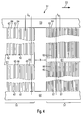
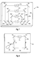
- FIG. 7 shows a substrate surface 45b of an optical diffraction component 15b, in which a surface wave source 47b emits surface waves of a frequency f 1 in a preferred direction 53b.
- a closed propagation path 95b is provided for the surface waves of the frequency f 0 via mirrors 91b, 92b, 93b and 94b, so that after passing through the closed propagation path 95b the surface waves finally pass through the surface source 47b again and are amplified there, similarly as in connection with the embodiment of Figure 6 has already been described.
- An interaction area for radiation to be deflected or diffracted is arranged between the mirrors 92b and 93b.
- the closed propagation paths 95b, 95b ', 95b "for surface waves of the frequencies f, f ', f " run together through the interaction area 17b and below divided by mirrors 93b “, 93b 'and 93b to again the surface wave sources 47b, 47b ', 47b “for the Frequencies f, f 'and f "to be supplied.
- the mirror 93b ' reflects Surface waves of frequency f ', while for surface waves the frequency f is also transparent.
- Each of the sources 47b, 47b 'and 47b "emits surface waves in a frequency spectrum, which depends on the control frequency changeable for the source within a certain range is.
- They are accordingly Deflection angle formed by the surface waves Lattice structure generated for the incident radiation can be varied in a particularly wide range.
- Sources 47b, 47b 'and 47 can be sequential in time are controlled so that the different deflection angles also be made available one after the other. Likewise it is possible to control the sources 47b, 47b 'and 47 "at the same time, so that the superposition of the corresponding surface waves with different wavelengths to form a multiple grating which leads the different deflection angles simultaneously provides.
- By overlaying the Surface waves with the frequencies f, f 'and f "and suitable Selecting these frequencies it is possible to use them in this way to overlay (to superpose) that a periodic lattice shape arises from the sinusoidal lattice shape differs.
- a so-called "blazed" Grating are provided in which certain diffraction orders specifically with higher diffraction intensity than other diffraction orders.
- Figures 6 and 7 are closed Propagation paths provided for the surface waves, the surface wave sources within the closed Paths of propagation lie.
- Figure 8 shows an embodiment in which on a surface 45c of a substrate 43c through mirrors 91c, 92c, 93c, 94c closed propagation path 95c is provided, wherein an interaction area between mirrors 94c and 91c 17c is arranged for incident radiation by the Propagation path 95c is traversed.
- a surface wave source 47c is outside the closed one Propagation path 95c arranged and emits surface waves in a preferred direction 53c.
- the surface wave source 47c on the substrate surface 45c arranged that the surface waves emitted by it on meet a mirror 97 located between mirrors 93c and 94c is arranged in the propagation path 95c.
- the Mirror 97 oriented so that it from the source 47c surface waves emitted in the direction 53c onto the Mirror 94c steers and thus already on the closed Propagation path 95c superimposed surface waves.
- For the surface waves coming from the mirror 93c mirror 97 is substantially transparent.
- a mirror resonator is thus provided by the mirrors 91c to 94c Surface waves formed, which by the source 47c with Surface waves that are fed through the mirror 97c in be coupled to the ring resonator.
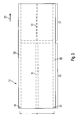
- FIG. 9 shows an optical diffraction component 15d with a Substrate surface 45d on which an interaction region 17d for deflecting radiation by means of surface waves is provided.
- the surface waves are from a source 47d emitted in a preferred direction 53d. That from the source 47d emitted surface waves hit one after the other on mirrors 91d, 101, 102, 103, 104, 92d, 93d and 94d.
- the Interaction area is between mirrors 102 and 103 on the one hand and the mirrors 101 and 104 on the other hand and is run through twice by the surface waves, namely once in a direction 105 of surface waves, that run from the mirror 101 to the mirror 102, and on the other hand in a direction opposite to direction 105
- Direction 106 of surface waves emitted by the mirror 103 run to the mirror 104.
- FIG. 10 shows a further diffraction-optical component 15e, in one direction from a surface wave source 47e 53e surface waves emitted on a substrate surface 50e also in a closed propagation path 95e circulate. Similar to the embodiment in FIG. 9 there is also an interaction region 17e from the surface waves in two different directions 105e and 106e go through, which, however, in contrast to the embodiment not opposite to FIG. 9 but orthogonal are oriented towards each other.
- the Source 47e sequentially emitted surface waves Mirrors 91e, 101e, 102e, 103e, 104e and 94e reflected, before being returned to source 47e like this can be seen from Figure 10.
- FIG. 11 shows an optical diffraction component 15f with a Substrate 43f, on its substrate surface 45f an interaction area 17f is provided.
- the area of interaction is hit several times by a beam of surface waves go through different directions. For this, one emits Surface wave source 47f surface waves in a preferred direction 53f directly on the interaction area 17f.
- the Surface wave beam After passing through the interaction area 17f, the Surface wave beam then at a mirror 91f by 90 ° deflected, hits another mirror 92f, is on deflected by 135 ° and passes through the interaction area 17f again, in a direction that is 135 ° rotates to direction 53f of the first passage through the interaction area is oriented.
- the beam After going through again of the interaction region 17f, the beam strikes another mirror 93f, is deflected by 135 °, meets another mirror 94f, on which it in turn is deflected by 135 ° and then the interaction area 17f passes through again in a direction that rotated by 90 ° with respect to the direction of the second pass is oriented.
- the beam After the third pass through the interaction area 17f the beam passes through a surface wave receiver 73f, which emits a signal which the Surface wave intensity after the third pass of the interaction area 17f.
- the beam After going through of the receiver 73f, the beam is in a separate Surface wave damper 111 absorbed.
- the Surface waves another surface wave source 113 arranged, which of the surface waves after the second Pass through the interaction region 17f and which is the intensity of these surface waves can increase so that for the third pass through the Interaction area 17f an adjustable higher intensity of surface waves is available.
- a controller for this diffraction optical component 15f can the outputs of the surface wave receivers 73f and 73f 'read out the power or swelling strength of the two Adjust sources 47f and 113 absolutely and relative to each other, with regard to a desired lattice structure, which by the surface waves in the interaction area 17f is formed.
- the intensity of the two surface wave sources 47f and 113 relative to each other be varied to diffraction efficiency in different To influence spatial directions.
- a diffraction-optical component 15g shown in FIG comprises a substrate 43g, on the surface 45g of which there is an interaction region 17g is provided within a Surface wave resonator is arranged in the standing Surface waves can be generated.
- a Surface wave resonator is arranged in the standing Surface waves can be generated.
- are on the Substrate surface two opposite surface wave mirrors 117 and 119 provided between which surface waves a predetermined frequency band and run or form a standing surface wave field there can.
- the interaction region 17g is arranged as well as further a surface wave source 47g through which the resonator is fed with surface waves.
- the interaction area 17g is of a continuous Light beam illuminates, which is thus in the interaction area sees a lattice structure, its lattice amplitude alternating in time with twice the frequency of the surface waves increases and decreases. The changes accordingly diffraction efficiency provided by this grating with the double frequency of surface waves.
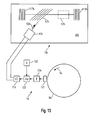
- FIG. 13 shows a further optical diffraction component 15h, in which in an interaction area 17h on a Substrate surface 45h by means of two facing one another Mirror 117h and 119h standing surface waves generated become.
- a surface wave source here, however 47h not arranged inside the resonator, but outside the same, in a preferred direction 53h of the source 47h emitted surface waves on a coupling mirror 97h which occurs within the resonator, i.e. between two mirrors 117h and 119h, is arranged and that of the Source 47h emits surface waves into the resonator where there is a field of standing surface waves formed.
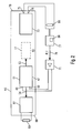
- the diffraction-optical component 15h shown in FIG. 13 is Part of a lighting system 2h, which acts as a light source has a sychrotron radiation source 5h, which is shown in FIG 13 is only shown schematically.
- a sychrotron radiation source 5h which is shown in FIG 13 is only shown schematically.
- the synchrotron 5h bundles of charged particles run in the direction of arrow 7h around and thereby do not emit on one in FIG represented beam position pulsed synchrotron radiation, which is directed to the interaction area 17h is.
- a sensor 121 is provided on the synchrotron 5h, which emits a measurement signal that the time sequence of the in the synchrotron rotating particle packets and thus the represents the temporal sequence of the radiation pulses.
- the Sensor 121 can, for example, be a beam pickup coil or be similar.
- the measurement signal provided by the sensor 121 becomes one Frequency control 77h supplied, which the frequency of the surface wave source 47h emits surface waves determined, the frequency f of the surface waves on the Half the frequency of the radiation pulses is set.
- the frequency signal output from the frequency controller 77h a phase shift controller 123 which has a phase ⁇ sets the surface waves emitted by the source 47h and then drives an amplifier 71h which finally feeds the surface wave source 47h.
- the phase shift control 123 makes the phase ⁇ dependent a signal registered by a radiation sensor 125 on.
- the radiation sensor 125 measures the intensity of a predetermined one Diffraction order on the interaction area 17h falling radiation.
- the diffraction grating provided to the interaction region 17h depends on the radiation sensor 125 output measurement signal the diffraction efficiency of the grating.
- the Phase control 123 sets the phase ⁇ in such a way that the diffraction efficiency is maximum.
- the phase shift controller 123 can also be used for this switch off the diffracted beam, i.e. the phase ⁇ so that the diffraction efficiency is minimal. This can happen, for example, that the phase ⁇ so is set that the radiation pulses always on the Interaction area meet when the amplitude of the standing Waves there has a value of essentially zero.
- the Phase shift control 123 driven such that the of the surface wave source 47h emits surface waves in the correct phase in those formed by mirrors 117h and 119h Surface wave resonator are coupled.
- the phase shift control 123 makes the phase angle ⁇ dependent from the radiation intensity sensor 125.
- the Radiation sensor 125 can be the intensity of the first or second or higher order diffracted radiation.
- phase shift control 123 the phase angle ⁇ does not depend on one Measurement signal of a radiation sensor sets, but in dependence from a measurement signal by a surface wave receiver is provided, which is the amplitude of the in surface waves occurring to the surface wave resonator detected.
- phase shift control depending from the measurement signal of a radiation sensor or a surface wave receiver is on all previously described Embodiments applicable in which either standing Surface waves or in a closed propagation path revolving surface waves are generated.
- directions of propagation were the surface waves mostly through mirrors, which is at an angle of 45 ° to the original direction of propagation the surface waves are arranged by 90 ° distracted from their original direction of propagation.
- This illustration has been made for the sake of simplicity. It however, it is noted that the propagation of surface waves often due to anisotropic effects in the material of the substrate is influenced or determined. That's why it is possible that the angular relationship between incident and falling beam upon reflection a mirror is not satisfied here with surface waves. Accordingly, an angle of incidence of surface waves is on a mirror is not always the same angle of reflection.
Landscapes
- Physics & Mathematics (AREA)
- General Physics & Mathematics (AREA)
- Nonlinear Science (AREA)
- Optics & Photonics (AREA)
- Diffracting Gratings Or Hologram Optical Elements (AREA)
- Exposure Of Semiconductors, Excluding Electron Or Ion Beam Exposure (AREA)
- Exposure And Positioning Against Photoresist Photosensitive Materials (AREA)
- Optical Head (AREA)
- Optical Modulation, Optical Deflection, Nonlinear Optics, Optical Demodulation, Optical Logic Elements (AREA)
Abstract
Description
96/report/exp/id32/id32.htm (29.01.2001) ist ein Röntgenstrahlchopper bekannt, welcher Röntgenstrahlung durch ein schaltbares optisches Gitter schaltet, welches durch Oberflächenwellen (SAW, SURFACE ACOUSTIC WAVES ) bereitgestellt ist. Allerdings ist bei dieser bekannten Anordnung eine Beugungsintensität des SAW-Gitters und damit eine Intensität des schaltbaren Strahls zu gering, als daß sich die dort beschriebene Oberflächenwellen-Bauanordnung zum wirtschaftlichen Einsatz in Lithographieverfahren eignen würde.
- Figur 1
- eine Ausführungsform eines erfindungsgemäßen Belichtungssystemes,
- Figur 2
- eine Ausführungsform einer erfindungsgemäßen beugungsoptischen Komponente,
- Figur 3
- eine schematische Auslegung einer Oberflächenwellenquelle zum Einsatz in der beugungsoptischen Komponente der Fig. 2,
- Figur 4
- eine Detaildarstellung der Oberflächenwellenquelle der Fig. 3,
- Figur 5
- schematische Graphen zur Erläuterung von Frequenzabhängigkeiten von Teilkomponenten der beugungsoptischen Komponente der Fig. 2,
- Figuren 6, 7, 8, 9, 10 und 12
- weitere Ausführungsformen der erfindungsgemäßen beugungsoptischen Komponente und
- Figur 13
- eine weitere Ausführungsform des erfindungsgemäßen Beleuchtungssystemes.
Claims (35)
- Beugungsoptische Komponente zur Bereitstellung einer strahlungsbeugenden Gitterstruktur, umfassend:dadurch gekennzeichnet, daß die Oberflächenwellenquelle (47) eine Richtcharakteristik aufweist und Oberflächenwellen in eine Vorzugsrichtung (53) stärker emittiert als in eine hierzu entgegengesetzte Richtung und wobei die in die Vorzugsrichtung (53) emittierten Oberflächenwellen die Gitterstruktur bereitstellen.eine Oberflächenwellen-Bauanordnung mit einem Substrat (43), einer mit einer einstellbaren Frequenz erregbaren Oberflächenwellenquelle (47) zur Erzeugung von Oberflächenwellen auf einer Oberfläche (45) des Substrats (43) und einem Wechselwirkungsbereich (17) der Substratoberfläche (45), der für eine Wechselwirkung der Strahlung mit einer durch die erzeugten Oberflächenwellen bereitgestellten Gitterstruktur vorgesehen ist,
- Beugungsoptische Komponente nach Anspruch 1 oder dem Oberbegriff von Anspruch 1, wobei die Oberflächenwellenquelle (47) einen elektroakustischen Wandler (51) umfaßt, der eine Elektrodenstruktur mit einer Vielzahl Teilelektroden (63, 64, 65, 66) aufweist, die mit Abstand zu benachbarten Teilelektroden (62, 67) angeordnet sind, wobei eine Mehrzahl von Bereichen (55, 57) vorgesehen ist, in denen die Teilelektroden periodisch angeordnet sind, und wobei sich die Anordnungsperioden (Λ1,Λ2) verschiedener Bereiche (55, 57) voneinander unterscheiden.
- Beugungsoptische Komponente nach Anspruch 1 oder 2 oder dem Oberbegriff von Anspruch 1, wobei die Oberflächenwellenquelle (47) einen elektroakustischen Wandler mit zwei Gruppen von Fingerelektroden (62, 65, 66) aufweist, wobei die Fingerelektroden (62, 65, 66) einer jeden Gruppe elektrisch leitend miteinander verbunden und die Fingerelektroden (62, 65, 66) unterschiedlicher Gruppen elektrisch voneinander isoliert sind, und wobei zwischen Paaren von Fingerelektroden (62, 65, 66) unterschiedlicher Gruppen wenigstens eine von den Fingerelektroden (62, 65, 66) jeweils elektrisch isolierte Zwischenelektrode (61) angeordnet ist.
- Beugungsoptische Komponente nach Anspruch 3, wobei zwischen Paaren von benachbarten Fingerelektroden (62, 65, 66) einer jeden Gruppe wenigstens eine Zweigelektrode (63, 64, 67) vorgesehen ist, die mit der Zwischenelektrode (61) elektrisch leitend verbunden ist.
- Beugungsoptische Komponente nach Anspruch 3 oder 4, wobei die Fingerelektroden (62, 65, 66) verschiedener Gruppen sich zueinander parallel versetzt erstrecken.
- Beugungsoptische Komponente nach Anspruch 5 in Verbindung mit Anspruch 4, wobei im wesentlichen einer jeden Fingerelektrode (62, 65, 66) eine Zweigelektrode (63, 64, 67) zugeordnet ist und sich die Fingerelektrode (62, 65, 66) und die ihr zugeordnete Zweigelektrode (63, 64, 67) auf einer gemeinsamen Geraden erstrecken.
- Beugungsoptische Komponente zur Bereitstellung einer strahlungsbeugenden Gitterstruktur, insbesondere nach einem der Ansprüche 1 bis 6, umfassend:eine Oberflächenwellen-Bauanordnung mit einem Substrat (43), einer mit einer einstellbaren Frequenz erregbare Oberflächenwellenquelle (47) zur Erzeugung von Oberflächenwellen auf einer Oberfläche (45) des Substrats (43) und einem Wechselwirkungsbereich (17) der Substratoberfläche (45), der für eine Wechselwirkung der Strahlung mit einer durch die erzeugten Oberflächenwellen bereitgestellten Gitterstruktur vorgesehen ist;einen Oberflächenwellenempfänger (73) zum Empfang von von der Oberflächenwellenquelle (47) erzeugten Oberflächenwellen und zur Abgabe eines eine Amplitude der Oberflächenwellen am Ort des Oberflächenwellenempfängers (73) angebenden Meßsignals; undeine die Frequenz (f) zur Erregung der Oberflächenwellenquelle (47) in Abhängigkeit von dem Meßsignal einstellende Steuerung (77).
- Beugungsoptische Komponente nach Anspruch 7, wobei die Steuerung (77) die Frequenz (f) derart einstellt, daß die Amplitude der empfangenen Oberflächenwellen im wesentlichen maximal ist.
- Beugungsoptische Komponente nach Anspruch 7 oder 8,
wobei eine Amplitude der von der Oberflächenwellenquelle (47) erzeugten Oberflächenwellen in Abhängigkeit von der Frequenz (f) zu deren Erregung einen ersten Verlauf aufweist,
wobei eine Größe des Meßsignals in Abhängigkeit von der Frequenz (f) einen zweiten Verlauf (84) aufweist,
wobei der erste Verlauf und der zweite Verlauf (84) jeweils eine um jeweils eine Mittelfrequenz beidseits mit einer Frequenzbreite (δf, Δf) abfallende Charakteristik aufweisen und
wobei die Frequenzbreite (Δf) des zweiten Verlaufs (84) größer ist als die Frequenzbreite (δf) des ersten Verlaufs. - Beugungsoptische Komponente nach Anspruch 9, wobei die Steuerung (77) die Frequenz (f) ferner in Abhängigkeit von dem zweiten Verlauf (84) steuert.
- Beugungsoptische Komponente zur Bereitstellung einer strahlungsbeugenden Gitterstruktur, insbesondere nach einem der Ansprüche 1 bis 10, umfassend:wobei der Oberflächenwellendämpfer (73, 87; 111, 111') einen akustoelektrischen Wandler zur Umwandlung von Energie der Oberflächenwellen am Ort des akustoelektrischen Wandlers in elektrische Energie umfaßt.eine Oberflächenwellen-Bauanordnung mit einem Substrat (43), einer Oberflächenwellenquelle (47) zur Erzeugung von Oberflächenwellen auf einer Oberfläche (45) des Substrats (43) und einem Wechselwirkungsbereich (17) der Substratoberfläche (45), der für eine Wechselwirkung der Strahlung mit einer durch die erzeugten Oberflächenwellen bereitgestellten Gitterstruktur vorgesehen ist;und einen ausserhalb des Wechselwirkungsbereichs (17) angeordneten Oberflächenwellendämpfer (73, 87; 111, 111') zum Dämpfen von Oberflächenwellen,
- Beugungsoptische Komponente nach Anspruch 11, wobei der akustoelektrische Wandler (73) wenigstens zwei Anschlüsse (75, 76) zur Bereitstellung der elektrischen Energie und ferner eine an die beiden Anschlüsse (75, 76) angeschlossene Widerstandsschaltung (81) zur Dissipation der elektrischen Energie umfaßt.
- Beugungsoptische Komponente nach Anspruch 12, wobei die Widerstandsschaltung (81) eine elektrische Impedanz aufweist, die an eine Impedanz des akustoelektrischen Wandlers (73) zwischen den beiden Anschlüssen (75, 76) derart angepasst ist, daß die in der Widerstandsschaltung (81) dissipierte Energie maximal ist.
- Beugungsoptische Komponente nach Anspruch 13, wobei die elektrische Impedanz der Widerstandsschaltung (81) und die elektrische Impedanz des akustoelektrischen Wandlers (73) zueinander konjugiert komplexe Werte aufweisen.
- Beugungsoptische Komponente nach einem der Ansprüche 11 bis 14, wobei die Oberflächenwellenquelle (47) einen elektroakustischen Wandler umfaßt, wobei der elektroakustischen Wandler der Oberflächenwellenquelle (47) und der akustoelektrischen Wandler des Oberflächenwellendämpfers (73) jeweils eine Elektrodenstruktur aufweisen, die jeweils bereichsweise eine Mehrzahl Teilelektroden (62, 63, 64, 65, 66, 76) umfaßt, welche periodisch mit Abstand zu benachbarten Teilelektroden angeordnet sind, wobei ein Bereich der Elektrodenstruktur des elektroakustischen Wandlers und ein Bereich der Elektrodenstruktur des akustoelektrischen Wandlers einander zugeordnet sind und wobei sich die Anordnungsperioden (Λ1,Λ2) der Teilelektroden (62, 63, 64, 65, 66, 76) der einander zugeordneten Bereiche unterscheiden.
- Beugungsoptische Komponente nach Anspruch 15, wobei sich die die Anordnungsperioden (Λ1, Λ2) der einander zugeordneten Bereiche um 0,01% bis 0,5%, insbesondere um 0,01% bis 0,05%, 0,05% bis 0,15% oder 0,15% bis 0,5%, unterscheiden.
- Beugungsoptische Komponente nach einem der Ansprüche 11 bis 16, wobei der akustoelektrischen Wandler des Oberflächenwellendämpfers (73) eine Richtcharakteristik aufweist und Oberflächenwellen, die aus einer Vorzugsrichtung (53) auf den Oberflächenwellendämpfer (73) treffen, stärker dämpft als aus einer hierzu entgegengesetzten Richtung eintreffende Oberflächenwellen.
- Beugungsoptische Komponente nach einem der Ansprüche 11 bis 17, wobei der Wechselwirkungsbereich (17) auf einer Verbindungslinie zwischen der Oberflächenwellenquelle (47) und dem Oberflächenwellendämpfer (73) angeordnet ist.
- Beugungsoptische Komponente nach einem der Ansprüche 11 bis 18, wobei die Oberflächenwellenquelle (74) auf einer Verbindungslinie zwischen dem Wechselwirkungsbereich (17) und dem Oberflächenwellendämpfer (87) angeordnet ist.
- Beugungsoptische Komponente zur Bereitstellung einer strahlungsbeugenden Gitterstruktur, insbesondere nach einem der Ansprüche 1 bis 19, umfassend:wobei der Wechselwirkungsbereich (17a; 17c) in dem geschlossenen Ausbreitungsweg liegt.eine Oberflächenwellen-Bauanordnung mit einem Substrat (43a; 43c), einer Oberflächenwellenquelle (47a; 47c) zur Erzeugung von Oberflächenwellen auf einer Oberfläche (45a; 45c) des Substrats (43a; 43c), einem Wechselwirkungsbereich (17a; 17c) der Substratoberfläche (45a; 45c), der für eine Wechselwirkung der Strahlung mit einer durch die erzeugten Oberflächenwellen bereitgestellten Gitterstruktur vorgesehen ist, undeine Mehrzahl von auf dem Substrat (43a; 43c) derart angeordneten Oberflächenwellenspiegeln (91, 92, 93, 94; 91c, 92c, 93c, 94c), daß sie einen geschlossenen Ausbreitungsweg für die Oberflächenwellen bereitstellen,
- Beugungsoptische Komponente nach Anspruch 20, wobei die Oberflächenwellenquelle (47a) eine Richtcharakteristik aufweist und Oberflächenwellen in eine Vorzugsrichtung (53a) stärker emittiert als in eine hierzu entgegengesetzte Richtung und wobei die Oberflächenwellenquelle (45a) in dem geschlossenen Ausbreitungsweg liegt.
- Beugungsoptische Komponente nach Anspruch 20, wobei die Oberflächenwellenquelle (47c) außerhalb des geschlossenen Ausbreitungswegs angeordnet ist und die von der Oberflächenwellenquelle (47c) emittierten Oberflächenwellen in den geschlossenen Ausbreitungsweg eingekoppelt werden.
- Beugungsoptische Komponente nach Anspruch 22, wobei ein weiterer Oberflächenwellenspiegel (87) zur Einkopplung der von der Oberflächenwellenquelle (47c) emittierten Oberflächenwellen in den geschlossenen Ausbreitungsweg vorgesehen ist.
- Beugungsoptische Komponente nach einem der Ansprüche 20 bis 23, wobei die Oberflächenwellenspiegel (91d, 92d, 93d, 94d, 101, 102, 103, 104) derart angeordnet sind, daß der Ausbreitungsweg den Wechselwirkungsbereich (17d) mehrmahls aus jeweils verschiedenen Richtungen (105, 106) durchläuft.
- Beugungsoptische Komponente zur Bereitstellung einer strahlungsbeugenden Gitterstruktur, insbesondere nach einem der Ansprüche 1 bis 24, umfassend:wobei die Gitterstruktur aus stehenden Oberflächenwellen gebildet ist.eine Oberflächenwellen-Bauanordnung mit einem Substrat (43g, 43h), wenigstens einer Oberflächenwellenquelle (47g, 47h) zur Erzeugung von Oberflächenwellen auf einer Oberfläche (45g, 45h) des Substrats, einem Wechselwirkungsbereich (17g, 17h) der Substratoberfläche (45g, 45h), der für eine Wechselwirkung der Strahlung mit einer durch die erzeugten Oberflächenwellen bereitgestellten Gitterstruktur vorgesehen ist, und
- Beugungsoptische Komponente nach Anspruch 25, wobei der Wechselwirkungsbereich (17g) auf einer Verbindungslinie zwischen der Oberflächenwellenquelle (47g) und einem Oberflächenwellenspiegel (119) angeordnet ist, der von der Oberflächenwellenquelle (47g) emittierte Oberflächenwellen zurück zu dem Wechselwirkungsbereich (17g) reflektiert.
- Beugungsoptische Komponente nach Anspruch 25 oder 26, wobei der Wechselwirkungsbereich (17h) innerhalb eines Oberflächenwellenresonators (117, 119) angeordnet ist, in den von der Oberflächenwellenquelle (47h) emittierte Oberflächenwellen eingekoppelt werden.
- Beugungsoptische Komponente nach Anspruch 27, wobei der Oberflächenwellenresonator durch Oberflächenwellenspiegel (117, 119) gebildet ist.
- Beugungsoptische Komponente nach Anspruch 27 oder 28, wobei ein weiterer Oberflächenwellenspiegel (97h) zur Einkopplung der von der Oberflächenwellenquelle (47h) emittierten Oberflächenwellen in den Oberflächenwellenresonator (117, 119) vorgesehen ist.
- Beleuchtungssystem, umfassend eine beugungsoptische Komponente nach einem der Ansprüche 25 bis 29 und eine (5, 11) Strahlungsquelle deren Strahlung auf den Wechselwirkungsbereich (17) der Oberflächenwellen-Bauanordnung gerichtet ist.
- Beleuchtungssystem, umfassend eine beugungsoptische Komponente nach einem der Ansprüche 25 bis 29, eine gepulste Strahlungsquelle (5h) deren Strahlung auf den Wechselwirkungsbereich (17h) der Oberflächenwellen-Bauanordnung gerichtet ist und deren Strahlungspulse mit der Oberflächenwellen-Bauanordnung derart synchronisiert sind, daß die Pulse innerhalb von Zeitperioden auf den Wechselwirkungsbereich (17h) treffen, wenn Amplituden der stehenden Oberflächenwellen einen vorbestimmten Schwellenwert überschreiten.
- Beleuchtungssystem nach Anspruch 31, wobei die Oberflächenwellenquelle (47) eine Ansteuervorrichtung (77h, 123) zur Einstellung einer Frequenz (f) und einer Phasenlage (Δϕ) der erzeugten Oberflächenwellen aufweist und wobei die Ansteuervorrichtung (77h, 123) die Frequenz (f) und die Phasenlage (Δϕ) in Abhängigkeit von einer Pulsfolge der Strahlungsquelle (5h) derart einstellt, daß eine Intensität an Strahlung, die durch die Gitterstruktur mit einer vorbestimmten Beugungsordnung gebeugt wird, einen vorbestimmten Wert, insbesondere im wesentlichen einen Maximalwert, aufweist.
- Beleuchtungssystem nach einem der Ansprüche 31 bis 32, wobei die Strahlungsquelle eine Synchrotronstrahlungsquelle (5h) ist.
- Belichtungssystem umfassend ein Beleuchtungssystem nach einem der Ansprüche 30 bis 33 sowie
wenigstens ein Kondensorsystem (25), eine mit einem abzubildenden Muster versehene Maske (27), ein Abbildungssystem (37) und einen Substrathalter (39),
wobei das Kondensorsystem (25) und die Maske (27) derart angeordnet sind, daß in dem Wechselwirkungsbereich (17) in unterschiedliche Raumrichtungen gebeugte Strahlung (+1, 0, -1) der Strahlungsquelle (5, 11) auf die Maske (27) gerichtet ist, und
wobei das Abbildungssystem (37) und der Substrathalter (39) derart angeordnet sind, daß von der Maske (27) reflektierte Strahlung auf ein an dem Substrathalter anbringbares Substrat (39) abgebildet ist. - Verfahren zur Herstellung eines Bauelements, umfassend wenigstens einen photolithographischen Schritt, wobei der photolithographische Schritt umfaßt:Bereitstellen des Belichtungssystems nach Anspruch 34,Anbringen eines mit einer strahlungsempfindlichen Schicht versehenen Substrats (39) an dem Substrathalter, undBelichten des strahlungsempfindlichen Substrats mit in unterschiedliche Raumrichtungen gebeugter Strahlung der Strahlungsquelle (5, 11).
Applications Claiming Priority (2)
| Application Number | Priority Date | Filing Date | Title |
|---|---|---|---|
| DE10113788 | 2001-03-21 | ||
| DE10113788A DE10113788A1 (de) | 2001-03-21 | 2001-03-21 | Beugungsoptische Komponente, Beleuchtungssystem und Belichtungssystem mit einer solchen beugungsoptischen Komponente und Belichtungsverfahren unter Verwendung eines solchen Belichtungssystems |
Publications (3)
| Publication Number | Publication Date |
|---|---|
| EP1243947A2 true EP1243947A2 (de) | 2002-09-25 |
| EP1243947A3 EP1243947A3 (de) | 2004-04-14 |
| EP1243947B1 EP1243947B1 (de) | 2009-05-06 |
Family
ID=7678407
Family Applications (1)
| Application Number | Title | Priority Date | Filing Date |
|---|---|---|---|
| EP02006299A Expired - Lifetime EP1243947B1 (de) | 2001-03-21 | 2002-03-20 | Beleuchtungs- und Belichtungssytem und -verfahren |
Country Status (5)
| Country | Link |
|---|---|
| US (1) | US6885491B2 (de) |
| EP (1) | EP1243947B1 (de) |
| JP (1) | JP4308475B2 (de) |
| KR (1) | KR20020075279A (de) |
| DE (2) | DE10113788A1 (de) |
Cited By (2)
| Publication number | Priority date | Publication date | Assignee | Title |
|---|---|---|---|---|
| EP1418463A1 (de) * | 2002-11-05 | 2004-05-12 | Matsushita Electric Industrial Co., Ltd. | UV akustooptisches Gerät und optische bildgebende Vorrichtung, die dasselbe verwendet |
| JP2004170940A (ja) * | 2002-11-05 | 2004-06-17 | Matsushita Electric Ind Co Ltd | 紫外光用音響光学素子及びこれを用いた光描画装置 |
Families Citing this family (8)
| Publication number | Priority date | Publication date | Assignee | Title |
|---|---|---|---|---|
| JP4093308B2 (ja) * | 2002-11-01 | 2008-06-04 | 富士通株式会社 | タッチパネル装置及び接触位置検出方法 |
| JP4652155B2 (ja) * | 2005-07-05 | 2011-03-16 | 株式会社ナノシステムソリューションズ | 露光装置及び露光方法 |
| KR101382481B1 (ko) | 2007-09-03 | 2014-04-09 | 삼성디스플레이 주식회사 | 표시 장치 |
| KR20150129429A (ko) * | 2014-05-12 | 2015-11-20 | 동우 화인켐 주식회사 | 대면적 근접 노광 장치 |
| US10107784B2 (en) | 2014-12-29 | 2018-10-23 | Concentric Meter Corporation | Electromagnetic transducer |
| WO2016109447A1 (en) | 2014-12-29 | 2016-07-07 | Concentric Meter Corporation | Fluid parameter sensor and meter |
| US10126266B2 (en) | 2014-12-29 | 2018-11-13 | Concentric Meter Corporation | Fluid parameter sensor and meter |
| DE102016217426A1 (de) * | 2016-09-13 | 2017-08-24 | Carl Zeiss Smt Gmbh | Strahlteiler |
Family Cites Families (46)
| Publication number | Priority date | Publication date | Assignee | Title |
|---|---|---|---|---|
| US3684892A (en) | 1970-10-15 | 1972-08-15 | Ibm | High gain wide band acoustic surface wave transducers using parametric upconversion |
| US4006967A (en) * | 1975-04-23 | 1977-02-08 | Battelle Memorial Institute | Directing optical beam |
| FR2336015A1 (fr) * | 1975-12-19 | 1977-07-15 | Thomson Csf | Dispositif de lecture acousto-electrique a deux dimensions d'une image optique |
| US4370030A (en) | 1980-05-27 | 1983-01-25 | Xerox Corporation | Extended resolution light deflector using surface acoustic waves |
| US4328472A (en) * | 1980-11-03 | 1982-05-04 | United Technologies Corporation | Acoustic guided wave devices |
| US4474467A (en) * | 1981-12-28 | 1984-10-02 | Itek Corporation | Wavefront sensor using a surface acoustic wave diffraction grating |
| US4521711A (en) | 1982-04-14 | 1985-06-04 | Clarion Co., Ltd. | Unidirectional transducer for a surface-acoustic-wave device and a method of making same |
| JPS60182426A (ja) | 1984-02-29 | 1985-09-18 | Omron Tateisi Electronics Co | 光偏向器 |
| EP0176786B1 (de) | 1984-09-03 | 1989-12-27 | Epprecht, Georg, Prof., Dr. | Wandler für SAW-Anordnung |
| US4910839A (en) | 1984-12-03 | 1990-03-27 | R.F. Monolithics, Inc. | Method of making a single phase unidirectional surface acoustic wave transducer |
| EP0222797A4 (de) | 1985-04-30 | 1988-04-27 | Univ Australian | Photoelastische modulatoren. |
| US4635008A (en) | 1985-11-19 | 1987-01-06 | Sperry Corporation | Dispersive SAW filter with tapered transducers |
| EP0259832A3 (en) * | 1986-09-09 | 1989-03-15 | Hitachi, Ltd. | Optical head |
| JPS63115131A (ja) | 1986-10-31 | 1988-05-19 | Nec Corp | 音響光学的モ−ド同期変調器 |
| JPH01252015A (ja) * | 1988-03-31 | 1989-10-06 | Toshiba Corp | 弾性表面波トランスデューサ |
| US5028101A (en) | 1988-07-19 | 1991-07-02 | Clarion Co., Ltd. | Surface-acoustic-wave device and notch filter device having a plurality of diode array channels |
| US5003822A (en) * | 1989-10-02 | 1991-04-02 | Joshi Shrinivas G | Acoustic wave microsensors for measuring fluid flow |
| US5264751A (en) | 1989-10-20 | 1993-11-23 | Thomson-Csf | Unilateral surface wave transducer |
| ATE113425T1 (de) | 1989-11-14 | 1994-11-15 | Siemens Ag | Oberflächenwellen-reflektorfilter. |
| US5073763A (en) | 1990-11-02 | 1991-12-17 | R.F. Monolithics, Inc. | Group single-phase unidirectional transducers with 3/8λand 5/8λ sampling |
| US5162689A (en) | 1991-05-01 | 1992-11-10 | Motorola, Inc. | Single-phase uni-directional acoustic wave transducer |
| JP2844968B2 (ja) | 1991-06-27 | 1999-01-13 | 日本電気株式会社 | 弾性表面波フィルタ用重み付け電極 |
| US5287036A (en) | 1992-03-02 | 1994-02-15 | Motorola, Inc. | Method and apparatus for acoustic wave inductance |
| US5438306A (en) | 1992-07-02 | 1995-08-01 | Kazuhiko Yamanouchi | Surface acoustic wave filter device with symmetrical electrode arrangement |
| US5334960A (en) | 1993-02-16 | 1994-08-02 | Motorola, Inc. | Conjugately matched acoustic wave transducers and method |
| US5406159A (en) | 1993-11-11 | 1995-04-11 | Rf Monolithics, Inc. | Surface acoustic wave gratings having selected reflectivity |
| BE1007876A4 (nl) * | 1993-12-17 | 1995-11-07 | Philips Electronics Nv | Stralingsbron-eenheid voor het opwekken van een bundel met twee polarisatierichtingen en twee frequenties. |
| US5646584A (en) | 1994-04-25 | 1997-07-08 | Advanced Saw Products Sa | Saw filter including electrodes of opposing polarity |
| EP0704967B1 (de) | 1994-09-28 | 2001-08-08 | Masao Takeuchi | Akustische Oberflächenwellenanordnung |
| JP2976273B2 (ja) * | 1995-03-24 | 1999-11-10 | 株式会社村田製作所 | 音響光学素子 |
| JP2920738B2 (ja) * | 1995-06-15 | 1999-07-19 | 株式会社村田製作所 | 音響光学偏向素子 |
| US5831492A (en) * | 1995-09-15 | 1998-11-03 | Sawtek Inc. | Weighted tapered spudt saw device |
| US5744721A (en) * | 1995-10-25 | 1998-04-28 | Hinds Instruments, Inc. | Electronic control system for an optical assembly |
| KR100188987B1 (ko) | 1996-09-06 | 1999-06-01 | 박원훈 | 각 셀의 개구가 일렬로 접속된 다중 채널 음향 광 변조기 |
| US5742425A (en) * | 1996-09-09 | 1998-04-21 | Crystal Technology, Inc. | Technique for electronically stabilizing the ouputs of acoustooptic devices |
| US5890789A (en) * | 1996-11-18 | 1999-04-06 | Minolta Co., Ltd. | Multi-beam emitting device having an acoustooptic element |
| TW490632B (en) * | 1996-12-25 | 2002-06-11 | Elo Touchsystems Inc | Grating transducer for acoustic touchscreen |
| US6208062B1 (en) * | 1997-08-18 | 2001-03-27 | X-Cyte, Inc. | Surface acoustic wave transponder configuration |
| US6147574A (en) | 1997-11-20 | 2000-11-14 | Murata Manufacturing Co., Ltd. | Unidirectional surface acoustic wave transducer and transversal-type saw filter having the same |
| US5973826A (en) | 1998-02-20 | 1999-10-26 | Regents Of The University Of California | Reflective optical imaging system with balanced distortion |
| US6142641A (en) | 1998-06-18 | 2000-11-07 | Ultratech Stepper, Inc. | Four-mirror extreme ultraviolet (EUV) lithography projection system |
| DE19850803A1 (de) * | 1998-11-04 | 2000-05-11 | Bosch Gmbh Robert | Sensoranordnung und ein Verfahren zur Ermittlung der Dichte und der Viskosität einer Flüssigkeit |
| JP2000180906A (ja) | 1998-12-16 | 2000-06-30 | Murata Mfg Co Ltd | 音響光学偏向素子 |
| US6033079A (en) | 1999-03-15 | 2000-03-07 | Hudyma; Russell | High numerical aperture ring field projection system for extreme ultraviolet lithography |
| DE10001291A1 (de) | 2000-01-14 | 2001-07-19 | Zeiss Carl | Adaptronischer Spiegel |
| US6285493B1 (en) * | 2000-07-31 | 2001-09-04 | Tasc, Inc. | Electro-acoustic-optical apparatus and method of calibrating same |
-
2001
- 2001-03-21 DE DE10113788A patent/DE10113788A1/de not_active Withdrawn
-
2002
- 2002-03-20 JP JP2002077756A patent/JP4308475B2/ja not_active Expired - Fee Related
- 2002-03-20 DE DE50213516T patent/DE50213516D1/de not_active Expired - Lifetime
- 2002-03-20 EP EP02006299A patent/EP1243947B1/de not_active Expired - Lifetime
- 2002-03-20 US US10/102,613 patent/US6885491B2/en not_active Expired - Fee Related
- 2002-03-21 KR KR1020020015403A patent/KR20020075279A/ko not_active Withdrawn
Cited By (4)
| Publication number | Priority date | Publication date | Assignee | Title |
|---|---|---|---|---|
| EP1418463A1 (de) * | 2002-11-05 | 2004-05-12 | Matsushita Electric Industrial Co., Ltd. | UV akustooptisches Gerät und optische bildgebende Vorrichtung, die dasselbe verwendet |
| JP2004170940A (ja) * | 2002-11-05 | 2004-06-17 | Matsushita Electric Ind Co Ltd | 紫外光用音響光学素子及びこれを用いた光描画装置 |
| US6903862B2 (en) | 2002-11-05 | 2005-06-07 | Matsushita Electric Industrial Co., Ltd. | Ultraviolet acoustooptic device and optical imaging apparatus using the same |
| CN100380224C (zh) * | 2002-11-05 | 2008-04-09 | 松下电器产业株式会社 | 紫外光声光器件和使用这种器件的光学成象设备 |
Also Published As
| Publication number | Publication date |
|---|---|
| DE50213516D1 (de) | 2009-06-18 |
| EP1243947B1 (de) | 2009-05-06 |
| JP4308475B2 (ja) | 2009-08-05 |
| US20030007712A1 (en) | 2003-01-09 |
| US6885491B2 (en) | 2005-04-26 |
| DE10113788A1 (de) | 2002-09-26 |
| EP1243947A3 (de) | 2004-04-14 |
| KR20020075279A (ko) | 2002-10-04 |
| JP2003037056A (ja) | 2003-02-07 |
Similar Documents
| Publication | Publication Date | Title |
|---|---|---|
| DE3116426C2 (de) | ||
| EP1243947A2 (de) | Beugungsoptische Komponente, Beleuchtungssystem und Belichtungssytem und -verfahren | |
| DE3013498C2 (de) | ||
| DE10135871B4 (de) | Wandler für Oberflächenwellen mit verbesserter Unterdrückung störender Anregung | |
| DE69628957T2 (de) | Wellenlangenumwandlungsvorrichtung mit einem nichgebeugten Strahl | |
| DE2821791A1 (de) | Einrichtung mit gitterreflektoren zur uebertragung akustischer oberflaechenwellen | |
| DE2045534B2 (de) | Oberflächenwellenfilter | |
| DE10314153A1 (de) | Oberflächenwellen-Anordnung zur breitbandigen Signalübertragung | |
| EP0276337B1 (de) | Blendenanordnung zur optoelektronischen Abtastung von Vorlagen | |
| DE1251368B (de) | Flachenhaft ausgebildeter Lichtmodulator zur Aufzeichnung von farbigen Licht , insbesondere B'ldsignalen bei welchem die Lichtmodu lation mit Hilfe von Farbbeugungsgittern erzielt wird, und optische Anordnung zur Auswertung solcherart gespeicherter Signale | |
| DE2831584C2 (de) | Wandler für akustische Oberflächenwellen und Filter auf der Basis dieser Wandler | |
| EP1028309B1 (de) | Optische Positionsmesseinrichtung | |
| EP1920387B1 (de) | Vorrichtung zur optischen aufspaltung und modulation von elektromagnetischer strahlung | |
| WO2011012503A1 (de) | Optisches system zum erzeugen eines lichtstrahls zur behandlung eines substrats | |
| DE2531151A1 (de) | Mit elastischen oberflaechenwellen arbeitende elektromechanische einrichtung | |
| EP0763715B1 (de) | Vorrichtung zur Filterung von Oberwellen-Signalanteilen | |
| DE2521695C3 (de) | Signalaufzeichnungsvorrichtung | |
| DE3221209C2 (de) | Gerät zur Untersuchung von Körpern durch Abtastung mittels Ultraschall | |
| DE60001001T2 (de) | Verfahren und vorrichtung zur formung des zeitlichen profils optischer quasimonochromatischer pulse | |
| DE69118682T2 (de) | Vorrichtung zur stabilisierung der reflektivität eines phasenkonjugierungsspiegels für hohe wiederrholungsfrequenz der mit stimulierter brillouin-streuung wirkt | |
| WO2001091293A1 (de) | Rekursives ofw-filter mit geringer chiplänge | |
| DE102008052410B4 (de) | Strahlungsoptisches Bauelement zur Beeinflussung von Strahlung in Bezug auf deren Wellenlängenspektrum | |
| DE4227340C2 (de) | Oberflächenwellen-Bauelement | |
| DE102019132935B3 (de) | Anordnung und Verfahren zur Manipulation oder Erzeugung von Röntgenpulsen | |
| DE102006040843A1 (de) | Vorrichtung zur optischen Aufspaltung und Modulation von elektromagnetischer Strahlung |
Legal Events
| Date | Code | Title | Description |
|---|---|---|---|
| PUAI | Public reference made under article 153(3) epc to a published international application that has entered the european phase |
Free format text: ORIGINAL CODE: 0009012 |
|
| AK | Designated contracting states |
Kind code of ref document: A2 Designated state(s): AT BE CH CY DE DK ES FI FR GB GR IE IT LI LU MC NL PT SE TR |
|
| AX | Request for extension of the european patent |
Free format text: AL;LT;LV;MK;RO;SI |
|
| RIC1 | Information provided on ipc code assigned before grant |
Ipc: 7G 02F 1/33 B Ipc: 7H 03H 9/145 B Ipc: 7G 02B 5/18 A Ipc: 7G 03F 7/20 B Ipc: 7G 02B 27/44 B |
|
| PUAL | Search report despatched |
Free format text: ORIGINAL CODE: 0009013 |
|
| RIC1 | Information provided on ipc code assigned before grant |
Ipc: 7G 02B 27/44 B Ipc: 7G 02F 1/01 B Ipc: 7G 02F 1/11 B Ipc: 7G 02B 5/18 A Ipc: 7H 03H 9/145 B Ipc: 7G 03F 7/20 B Ipc: 7G 02F 1/33 B |
|
| AK | Designated contracting states |
Kind code of ref document: A3 Designated state(s): AT BE CH CY DE DK ES FI FR GB GR IE IT LI LU MC NL PT SE TR |
|
| AX | Request for extension of the european patent |
Extension state: AL LT LV MK RO SI |
|
| 17P | Request for examination filed |
Effective date: 20040506 |
|
| 17Q | First examination report despatched |
Effective date: 20040608 |
|
| RAP1 | Party data changed (applicant data changed or rights of an application transferred) |
Owner name: CARL-ZEISS-STIFTUNG TRADING AS CARL ZEISS Owner name: CARL ZEISS |
|
| AKX | Designation fees paid |
Designated state(s): DE FR GB NL |
|
| GRAP | Despatch of communication of intention to grant a patent |
Free format text: ORIGINAL CODE: EPIDOSNIGR1 |
|
| RTI1 | Title (correction) |
Free format text: ILLUMINATION SYSTEM, EXPOSURE SYSTEM AND EXPOSURE METHOD |
|
| GRAS | Grant fee paid |
Free format text: ORIGINAL CODE: EPIDOSNIGR3 |
|
| GRAA | (expected) grant |
Free format text: ORIGINAL CODE: 0009210 |
|
| AK | Designated contracting states |
Kind code of ref document: B1 Designated state(s): DE FR GB NL |
|
| REG | Reference to a national code |
Ref country code: GB Ref legal event code: FG4D Free format text: NOT ENGLISH |
|
| REF | Corresponds to: |
Ref document number: 50213516 Country of ref document: DE Date of ref document: 20090618 Kind code of ref document: P |
|
| NLV1 | Nl: lapsed or annulled due to failure to fulfill the requirements of art. 29p and 29m of the patents act | ||
| PG25 | Lapsed in a contracting state [announced via postgrant information from national office to epo] |
Ref country code: NL Free format text: LAPSE BECAUSE OF FAILURE TO SUBMIT A TRANSLATION OF THE DESCRIPTION OR TO PAY THE FEE WITHIN THE PRESCRIBED TIME-LIMIT Effective date: 20090506 |
|
| PLBE | No opposition filed within time limit |
Free format text: ORIGINAL CODE: 0009261 |
|
| STAA | Information on the status of an ep patent application or granted ep patent |
Free format text: STATUS: NO OPPOSITION FILED WITHIN TIME LIMIT |
|
| 26N | No opposition filed |
Effective date: 20100209 |
|
| GBPC | Gb: european patent ceased through non-payment of renewal fee |
Effective date: 20100320 |
|
| REG | Reference to a national code |
Ref country code: FR Ref legal event code: ST Effective date: 20101130 |
|
| PG25 | Lapsed in a contracting state [announced via postgrant information from national office to epo] |
Ref country code: FR Free format text: LAPSE BECAUSE OF NON-PAYMENT OF DUE FEES Effective date: 20100331 |
|
| PG25 | Lapsed in a contracting state [announced via postgrant information from national office to epo] |
Ref country code: GB Free format text: LAPSE BECAUSE OF NON-PAYMENT OF DUE FEES Effective date: 20100320 |
|
| PGFP | Annual fee paid to national office [announced via postgrant information from national office to epo] |
Ref country code: DE Payment date: 20130321 Year of fee payment: 12 |
|
| REG | Reference to a national code |
Ref country code: DE Ref legal event code: R119 Ref document number: 50213516 Country of ref document: DE |
|
| REG | Reference to a national code |
Ref country code: DE Ref legal event code: R119 Ref document number: 50213516 Country of ref document: DE Effective date: 20141001 |
|
| PG25 | Lapsed in a contracting state [announced via postgrant information from national office to epo] |
Ref country code: DE Free format text: LAPSE BECAUSE OF NON-PAYMENT OF DUE FEES Effective date: 20141001 |