EP1243843A2 - LED-Signalmodul - Google Patents
LED-Signalmodul Download PDFInfo
- Publication number
- EP1243843A2 EP1243843A2 EP02090004A EP02090004A EP1243843A2 EP 1243843 A2 EP1243843 A2 EP 1243843A2 EP 02090004 A EP02090004 A EP 02090004A EP 02090004 A EP02090004 A EP 02090004A EP 1243843 A2 EP1243843 A2 EP 1243843A2
- Authority
- EP
- European Patent Office
- Prior art keywords
- circuit board
- main surface
- led
- signal module
- led signal
- Prior art date
- Legal status (The legal status is an assumption and is not a legal conclusion. Google has not performed a legal analysis and makes no representation as to the accuracy of the status listed.)
- Granted
Links
Images


Classifications
-
- F—MECHANICAL ENGINEERING; LIGHTING; HEATING; WEAPONS; BLASTING
- F21—LIGHTING
- F21V—FUNCTIONAL FEATURES OR DETAILS OF LIGHTING DEVICES OR SYSTEMS THEREOF; STRUCTURAL COMBINATIONS OF LIGHTING DEVICES WITH OTHER ARTICLES, NOT OTHERWISE PROVIDED FOR
- F21V29/00—Protecting lighting devices from thermal damage; Cooling or heating arrangements specially adapted for lighting devices or systems
- F21V29/50—Cooling arrangements
- F21V29/70—Cooling arrangements characterised by passive heat-dissipating elements, e.g. heat-sinks
- F21V29/74—Cooling arrangements characterised by passive heat-dissipating elements, e.g. heat-sinks with fins or blades
- F21V29/76—Cooling arrangements characterised by passive heat-dissipating elements, e.g. heat-sinks with fins or blades with essentially identical parallel planar fins or blades, e.g. with comb-like cross-section
- F21V29/763—Cooling arrangements characterised by passive heat-dissipating elements, e.g. heat-sinks with fins or blades with essentially identical parallel planar fins or blades, e.g. with comb-like cross-section the planes containing the fins or blades having the direction of the light emitting axis
-
- F—MECHANICAL ENGINEERING; LIGHTING; HEATING; WEAPONS; BLASTING
- F21—LIGHTING
- F21V—FUNCTIONAL FEATURES OR DETAILS OF LIGHTING DEVICES OR SYSTEMS THEREOF; STRUCTURAL COMBINATIONS OF LIGHTING DEVICES WITH OTHER ARTICLES, NOT OTHERWISE PROVIDED FOR
- F21V29/00—Protecting lighting devices from thermal damage; Cooling or heating arrangements specially adapted for lighting devices or systems
- F21V29/50—Cooling arrangements
- F21V29/70—Cooling arrangements characterised by passive heat-dissipating elements, e.g. heat-sinks
-
- F—MECHANICAL ENGINEERING; LIGHTING; HEATING; WEAPONS; BLASTING
- F21—LIGHTING
- F21V—FUNCTIONAL FEATURES OR DETAILS OF LIGHTING DEVICES OR SYSTEMS THEREOF; STRUCTURAL COMBINATIONS OF LIGHTING DEVICES WITH OTHER ARTICLES, NOT OTHERWISE PROVIDED FOR
- F21V29/00—Protecting lighting devices from thermal damage; Cooling or heating arrangements specially adapted for lighting devices or systems
- F21V29/50—Cooling arrangements
- F21V29/70—Cooling arrangements characterised by passive heat-dissipating elements, e.g. heat-sinks
- F21V29/74—Cooling arrangements characterised by passive heat-dissipating elements, e.g. heat-sinks with fins or blades
-
- F—MECHANICAL ENGINEERING; LIGHTING; HEATING; WEAPONS; BLASTING
- F21—LIGHTING
- F21V—FUNCTIONAL FEATURES OR DETAILS OF LIGHTING DEVICES OR SYSTEMS THEREOF; STRUCTURAL COMBINATIONS OF LIGHTING DEVICES WITH OTHER ARTICLES, NOT OTHERWISE PROVIDED FOR
- F21V5/00—Refractors for light sources
- F21V5/04—Refractors for light sources of lens shape
-
- H—ELECTRICITY
- H05—ELECTRIC TECHNIQUES NOT OTHERWISE PROVIDED FOR
- H05K—PRINTED CIRCUITS; CASINGS OR CONSTRUCTIONAL DETAILS OF ELECTRIC APPARATUS; MANUFACTURE OF ASSEMBLAGES OF ELECTRICAL COMPONENTS
- H05K1/00—Printed circuits
- H05K1/02—Details
- H05K1/0201—Thermal arrangements, e.g. for cooling, heating or preventing overheating
- H05K1/0203—Cooling of mounted components
- H05K1/0204—Cooling of mounted components using means for thermal conduction connection in the thickness direction of the substrate
- H05K1/0206—Cooling of mounted components using means for thermal conduction connection in the thickness direction of the substrate by printed thermal vias
-
- F—MECHANICAL ENGINEERING; LIGHTING; HEATING; WEAPONS; BLASTING
- F21—LIGHTING
- F21V—FUNCTIONAL FEATURES OR DETAILS OF LIGHTING DEVICES OR SYSTEMS THEREOF; STRUCTURAL COMBINATIONS OF LIGHTING DEVICES WITH OTHER ARTICLES, NOT OTHERWISE PROVIDED FOR
- F21V17/00—Fastening of component parts of lighting devices, e.g. shades, globes, refractors, reflectors, filters, screens, grids or protective cages
- F21V17/10—Fastening of component parts of lighting devices, e.g. shades, globes, refractors, reflectors, filters, screens, grids or protective cages characterised by specific fastening means or way of fastening
- F21V17/16—Fastening of component parts of lighting devices, e.g. shades, globes, refractors, reflectors, filters, screens, grids or protective cages characterised by specific fastening means or way of fastening by deformation of parts; Snap action mounting
- F21V17/164—Fastening of component parts of lighting devices, e.g. shades, globes, refractors, reflectors, filters, screens, grids or protective cages characterised by specific fastening means or way of fastening by deformation of parts; Snap action mounting the parts being subjected to bending, e.g. snap joints
-
- F—MECHANICAL ENGINEERING; LIGHTING; HEATING; WEAPONS; BLASTING
- F21—LIGHTING
- F21W—INDEXING SCHEME ASSOCIATED WITH SUBCLASSES F21K, F21L, F21S and F21V, RELATING TO USES OR APPLICATIONS OF LIGHTING DEVICES OR SYSTEMS
- F21W2111/00—Use or application of lighting devices or systems for signalling, marking or indicating, not provided for in codes F21W2102/00 – F21W2107/00
-
- F—MECHANICAL ENGINEERING; LIGHTING; HEATING; WEAPONS; BLASTING
- F21—LIGHTING
- F21Y—INDEXING SCHEME ASSOCIATED WITH SUBCLASSES F21K, F21L, F21S and F21V, RELATING TO THE FORM OR THE KIND OF THE LIGHT SOURCES OR OF THE COLOUR OF THE LIGHT EMITTED
- F21Y2115/00—Light-generating elements of semiconductor light sources
- F21Y2115/10—Light-emitting diodes [LED]
-
- H—ELECTRICITY
- H05—ELECTRIC TECHNIQUES NOT OTHERWISE PROVIDED FOR
- H05K—PRINTED CIRCUITS; CASINGS OR CONSTRUCTIONAL DETAILS OF ELECTRIC APPARATUS; MANUFACTURE OF ASSEMBLAGES OF ELECTRICAL COMPONENTS
- H05K2201/00—Indexing scheme relating to printed circuits covered by H05K1/00
- H05K2201/10—Details of components or other objects attached to or integrated in a printed circuit board
- H05K2201/10007—Types of components
- H05K2201/10106—Light emitting diode [LED]
-
- H—ELECTRICITY
- H05—ELECTRIC TECHNIQUES NOT OTHERWISE PROVIDED FOR
- H05K—PRINTED CIRCUITS; CASINGS OR CONSTRUCTIONAL DETAILS OF ELECTRIC APPARATUS; MANUFACTURE OF ASSEMBLAGES OF ELECTRICAL COMPONENTS
- H05K3/00—Apparatus or processes for manufacturing printed circuits
- H05K3/0058—Laminating printed circuit boards onto other substrates, e.g. metallic substrates
- H05K3/0061—Laminating printed circuit boards onto other substrates, e.g. metallic substrates onto a metallic substrate, e.g. a heat sink
-
- H—ELECTRICITY
- H10—SEMICONDUCTOR DEVICES; ELECTRIC SOLID-STATE DEVICES NOT OTHERWISE PROVIDED FOR
- H10W—GENERIC PACKAGES, INTERCONNECTIONS, CONNECTORS OR OTHER CONSTRUCTIONAL DETAILS OF DEVICES COVERED BY CLASS H10
- H10W90/00—Package configurations
Definitions
- the present invention relates to an LED signal module, in which in particular the LED components at least are dustproof and preferably also encapsulated watertight.
- LEDs Light-emitting diodes
- the LED signal modules that are usually on Instead of conventional light sources, a plurality of LED components included as illuminants are on site extreme and aggressive climatic, chemical, biological and exposed to mechanical environmental conditions against interference from this unfriendly Conditions.
- LEDs Signaling devices based on LEDs must be matched to the properties of these lamps. So there are influences that occur when using conventional signal lamps and light sources, such as light bulbs or propane lights, are not critical, but when using LEDs as Illuminants are functionally important. Nice in the prevention or removal of dirt there are differences due to dust and the like. Let it be with conventional signal generators, the components that Have an influence on the light intensity, such as Lamp, the lens and the color filter, comparatively easy to clean mechanically by wiping. In LED signal modules usually form the LEDs together with imaging optical components an optical system whose Individual parts for cleaning measures are difficult to access or are sensitive to it.
- Another influencing factor is the heat dissipation from the LEDs whose lifespan is influenced by the chip temperature during operation is. The better the heat dissipation, the bigger the Lifetime of the LEDs.
- the present invention is based on the object LED signal module to provide that against the above sufficient harmful environmental influences is protected. Furthermore, such a module should be as possible have low thermal stress on the LED components.
- the first task is performed by an LED signal module solved the features of claim 1 or 4.
- Advantage Developments of the module are the subject of the claims 2, 3 and 5 to 14.
- a first LED signal module is on a first main surface of an electrically insulating printed circuit board a plurality of LED components and on one of the first main surface opposite second main surface of the Printed circuit board a cooling device for cooling the LED components arranged.
- Conductor tracks for interconnecting the LED components are by means of a plurality of at least dust-tight, preferably also waterproof heat-conducting bushings through the circuit board from the first main surface to plated through the second main surface.
- the thermally conductive bushings are with the cooling device thermally connected.
- Another LED signal module is on a first main surface of a metal core circuit board A plurality of LED components, a socket strip and one Conductor structure for interconnecting the LED components and the socket strip arranged.
- a cooling device On one of the first main areas opposite second main surface of the circuit board a cooling device arranged.
- the metal core board points in the area of connection contacts of the socket strip one or several openings through which the female header accessible for a power strip from the second main surface is.
- the female header is by means of a sealing layer at least dustproof from the area in which the LED components are located, separated.
- a low thermal load on the LED components that means a slight increase in temperature of the LED components in the Operation of the module is advantageously achieved by that are essentially on the circuit board as heat sources only the LED components are located and these also by means of a cooling device (for example a metal heat sink known Type) that are in thermal contact with conductor tracks for Interconnection of the LED components or with the metal core board stands.
- a cooling device for example a metal heat sink known Type
- Other heat-producing components in particular an energy supply and / or control device, are largely removed from the circuit board arranged.
- FIG. 1 In the embodiment of Figure 1 is a circuit board 10 provided an electrically insulating support plate 14 has. On a first main surface 11 of the carrier plate 14, an electrical conductor track structure 4 is applied for connection and electrical power supply for a Plurality of LED components motivated on the first main surface 2 serves.
- the LED components 2 preferably have a surface-mountable LED design. But radial designs can also be used of LED components used in Push-through mounting on the circuit board 10 are attached. So-called chip-on-board assembly is also conceivable, at the unhoused LED chips directly onto the printed circuit board 10 to be assembled.
- the main surface 12 of the printed circuit board 10 is a cooling device 3, for example a conventional metallic heat sink with cooling fins, arranged. This is with the electrical Conductor tracks 4 over at least dustproof, preferably also waterproof thermally conductive bushings 50 and one electrically insulating heat-conducting film 8 connected.
- the heat-conducting bushings 50 which are made of, for example Metallic material are made, and the thermal foil 8, for example a commercially available film with the Guarantee HI-FLOW TM 625 from Bergquist advantageously a good derivation of the operation of the LED components generated by this heat loss, thereby the temperature increase of the LED components during operation and thus the aging of the LED components is reduced as much as possible is.
- the electrical connection contacts 7, for example spring contacts for pins of a connector strip, are electrically conductive by means of dustproof Feedthroughs 51 with those arranged on the first main surface 11 electrical conductor tracks 4 electrically connected.
- a metal core circuit board 100 provided with an electrically insulating Layer 104 is provided. On the insulating layer 104 is located, a plurality of LED components 2, one Female connector 6 and a conductor track structure 4 for electrical Interconnection of the LED components 2 and the socket strip 6. On the opposite of the insulating layer 104 A cooling device 3 is arranged on the side of the printed circuit board, which are preferably in direct contact with the metal core Metal core board 100 stands.
- the metal core board 100 has in the area of connection contacts 7 of the socket strip 6, several openings 103, for Example holes on the spring contacts 7 of the Socket strip 6 for contact pins of a plug strip from the Heatsink side is accessible.
- the socket strip 6 is by means of a sealing layer 9, for example a plastic encapsulation, dustproof from the area where the LED components 2 are located, separated.
- the schematic sectional view according to FIG. 3 is in principle shown as an arrangement according to Figure 1 or 2 in a module housing is arranged.
- the printed circuit board 10 or 100 with the LED components 2, the socket strip 6 and the Heat sink 3 is located in a module carrier 20.
- Between Module carrier 20 and circuit board 10, 100 is dust-proof Connection trained.
- On a circumferential side wall of the Module carrier 20 is an optical plate 30, for example a Lens holder, which spans the LED components 2.
- the edge area of the optical plate 30 forms with the peripheral one Side wall of the module carrier 20 a dustproof Connection out, so that the interior of the module housing, the essentially from the circuit board 10,100, the module carrier 20 and the optical plate 30 is formed, dustproof from the Environment is separated.
- the module carrier and the optical plate are preferably made both made of transparent plastic, which means that in operation resulting stray light from the LEDs for improved side visibility of the signal leads.
- a cover glass 60 is preferably located above the optical plate 30 and / or a lens 70, which advantageously achieved a reduction in incident UV radiation which leads to an accelerated degradation of the LED components would lead.
- FIG 4 is a detailed section of a preferred Execution form of the housing seal is shown schematically.
- a module carrier 20, which here is essentially the shape a carrier ring running around the circuit board 10 or has frame, is on the end face of its circumferential Side wall 24 is provided with a fold 21, on the bearing surface 22 the circuit board 10 is placed. Between the Printed circuit board 10 and the support surface on the side wall 24 is the edge of the heat-conducting film 8, which is on this Place the function of a sealing layer fulfilled.
- the circuit board 10 is in areas between the LED components 2 the optical plate 30, for example a lens plate, on, which is screwed to the module carrier 20, for example and thereby the edge of the circuit board on the Side wall 24 of the module carrier 20 presses.
- the LED components 2 find space 30 in recesses 34 of the optical plate.
- the optics plate has a circumferential edge Bead 31, which is based on the module carrier 20 facing underside of the optical plate in the direction of the module carrier 20 extends and over the entire scope of the Side wall 24 engages and partially overlaps it.
- the bevel 25 of the side wall 24 is for this particularly preferably less steep than the bevel 33 of FIG Bead 31.
- module carrier 20 can of course also be used have a circumferential bead, which then over the outer Side wall of the optical plate 30 engages.
- the module carrier 20 has a receiving element 26 for the heat sink 3, with which the heat sink 3 against the Thermally conductive film 8 is pressed.
- Subregions 35 of the printed circuit board 10 are located in the module facing side of the optical plate 30 between the LED components 2 on the first main surface 11 of the printed circuit board 10 and press the circuit board 10 against the fold 21 of the module carrier 20th
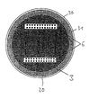
- FIG. 5 shows a schematic representation of the Back of a fully assembled assembly in which the heat sink 3 with cutouts for two socket strips 6, the bottom the circumferential side end wall 24 of the module carrier 20 and the bead 31 of the optical plate 30 can be seen.
- the socket strips 6 are used to connect the LED components 2 with externally arranged electronic components to control them.
- On the circuit board are particularly preferred only the LED components 2 and the socket strips 6 mounted so that no additional heat loss nearby of the LED components is created by control electronics. Farther this arrangement advantageously allows a separate one Exchange of LED signal lamp and control electronics.
Landscapes
- Engineering & Computer Science (AREA)
- General Engineering & Computer Science (AREA)
- Microelectronics & Electronic Packaging (AREA)
- Arrangement Of Elements, Cooling, Sealing, Or The Like Of Lighting Devices (AREA)
- Led Devices (AREA)
- Planar Illumination Modules (AREA)
- Led Device Packages (AREA)
- Cooling Or The Like Of Electrical Apparatus (AREA)
- Cooling Or The Like Of Semiconductors Or Solid State Devices (AREA)
Abstract
Description
Claims (14)
- LED-Signalmodul (1), bei deman einer ersten Hauptfläche (11) einer elektrisch isolierenden Leiterplatte (10) eine Mehrzahl von LED-Bauelementen (2) und an einer der ersten Hauptfläche (11) gegenüberliegenden zweiten Hauptfläche (12) der Leiterplatte (10) eine Kühleinrichtung (3) angeordnet ist,auf der ersten Hauptfläche (11) angeordnete, insbesondere zur Verschaltung der LED-Bauelemente (2) vorgesehene Leiterbahnen (4) mittels einer Mehrzahl von staubdichten wärmeleitenden Durchführungen (50) durch die Leiterplatte (10) mit der zweiten Hauptfläche (12) der Leiterplatte (10) wärmeleitend verbunden sind unddie wärmeleitenden Durchführungen (5) mit der Kühleinrichtung (3) wärmeleitend verbunden sind.
- LED-Signalmodul nach Anspruch 1, bei dem an der zweiten Hauptfläche (12) der Leiterplatte eine Buchsenleiste (6) angeordnet ist, deren elektrische Anschlußkontakte (7) mittels staubdichten elektrisch leitenden Durchführungenen (51) mit den auf der ersten Hauptfläche (11) angeordneten elektrischen Leiterbahnen (4) verbunden sind.
- LED-Signalmodul nach einem der vorangehenden Ansprüche, bei dem zwischen der zweiten Hauptfläche (12) der Leiterplatte (10) und der Kühleinrichtung (3) eine elektrisch isolierende Wärmeleitfolie (8) angeordnet ist.
- LED-Signalmodul, bei deman einer ersten Hauptfläche (101) einer Metallkern-Leiterplatte (100) eine Mehrzahl von LED-Bauelementen (2), eine Buchsenleiste (6) und eine Leiterbahnstruktur (4) zur Verschaltung der LED-Bauelemente (2) und der Buchsenleiste (6) angeordnet ist,an einer der ersten Hauptfläche (101) gegenüberliegenden zweiten Hauptfläche (102) der Leiterplatte (100) eine Kühleinrichtung (3) angeordnet ist,die Metallkernplatine (100) im Bereich von Anschlußkontakten (7) der Buchsenleiste (6) einen oder mehrere Durchbrüche (103) aufweist, über den bzw. die die Buchsenleiste (6) für eine Steckerleiste von der zweiten Hauptfläche (102) der Leiterplatte (10) her zugänglich ist, unddie Buchsenleiste (6) mittels einer Dichtungsschicht (9) staubdicht von dem Bereich, in dem sich die LED-Bauelemente (2) befinden, abgetrennt ist.
- LED-Signalmodul nach einem der vorangehenden Ansprüche, bei der ein umlaufender Rand (13) der elektrischen Leiterplatte (10) in einen umlaufenden Falz (21) eines Modulträgers (20) eingepaßt ist und zwischen der Leiterplatte (10) und einer Auflagefläche (22) des Falzes (21) für die Leiterplatte (10) ein umlaufendes staubdichtes Dichtungselement (23) angeordnet ist.
- LED-Signalmodul nach Anspruch 3 und 5, bei dem ein umlaufender Rand der Wärmeleitfolie (8) als umlaufendes Dichtungselement (23) genutzt ist.
- LED-Signalmodul nach einem der vorangehenden Ansprüche, bei dem an der ersten Hauptfläche (11) der Leiterplatte (10) eine Optikplatte (30), insbesondere ein Linsenträger angeordnet ist, die auf einer um die Leiterplatte (10) umlaufenden Seitenwand (24) des Modulträgers (20) oder ,auf einem um die Mehrzahl von LED-Bauelementen (2) umlaufenden Rand der Leiterplatte (10) aufsitzt und mit dieser bzw. diesem eine staubdichte Gehäusedichtung aufweist.
- LED-Signalmodul nach Anspruch 7, bei der die Optikplatte (30) eine über die Seitenwand (24) des Modulträgers (20) bzw. über die Stirnseite der Leiterplatte (10) greifende umlaufende Wulst (31) aufweist, die mit der Seitenwand (24) des Modulträgers (20) bzw. mit der Stirnseite der Leiterplatte (10) die staubdichte Gehäusedichtung (40) ausbildet.
- LED-Signalmodul nach Anspruch 8, bei dem sowohl die Seitenwand (24) des Modulträgers (20) bzw. die Stirnseite der Leiterplatte (10) als auch die umlaufende Innenseite (32) der Wulst (31) abgeschrägt ist, wobei die Schräge (33) der Wulst (31) steiler ist als die Schräge (25) der Seitenwand (24) des Modulträgers (20) bzw. der Stirnseite der Leiterplatte (10) und die beiden Schrägen (25,33) aufeinandergepresst sind und die staubdichte Gehäusedichtung (40) ausbilden.
- LED-Signalmodul nach Anspruch 7, 8 oder 9, bei dem Teilbereiche (35) der der Leiterplatte (10) zugewandten Seite der Optikplatte (30) zwischen den LED-Bauelementen (2) auf der ersten Hauptfläche (11) der Leiterplatte (10) aufliegt und die Leiterplatte (10) gegen den Falz (21) des Modulträgers (20) drückt.
- LED-Signalmodul nach einem der Ansprüche 7 bis 10, bei dem der Modulträger (20) und die Optikplatte (30) aus einem transparenten Kunststoffmaterial gefertigt ist.
- LED-Signalmodul nach einem der Ansprüche 7 bis 11, bei dem der Optikplatte (30) in Abstrahlrichtung des Moduls ein Abschlußglas (60) nachgeordnet ist.
- LED-Signalmodul nach einem der Ansprüche 7 bis 12, bei dem der Optikplatte (30) in Abstrahlrichtung des Moduls eine Streuscheibe (70) nachgeordnet ist.
- LED-Signalmodul nach einem der vorangehenden Ansprüche, bei dem auf der Leiterplatte (10) im Wesentlichen nur die LED-Bauelemente (2) im Betrieb des Moduls wesentliche Verlustwärme produzieren und weitere verlustwärmeproduzierende Bauelemente, insbesondere einer Energieversorgungs- und/oder Steuereinrichtung, weitestgehend entfernt von der Leiterplatte (10) angeordnet sind.
Applications Claiming Priority (2)
| Application Number | Priority Date | Filing Date | Title |
|---|---|---|---|
| DE10102353A DE10102353B4 (de) | 2001-01-19 | 2001-01-19 | LED-Signalmodul |
| DE10102353 | 2001-01-19 |
Publications (3)
| Publication Number | Publication Date |
|---|---|
| EP1243843A2 true EP1243843A2 (de) | 2002-09-25 |
| EP1243843A3 EP1243843A3 (de) | 2004-12-15 |
| EP1243843B1 EP1243843B1 (de) | 2008-12-31 |
Family
ID=7671117
Family Applications (1)
| Application Number | Title | Priority Date | Filing Date |
|---|---|---|---|
| EP02090004A Expired - Lifetime EP1243843B1 (de) | 2001-01-19 | 2002-01-08 | LED-Signalmodul |
Country Status (5)
| Country | Link |
|---|---|
| EP (1) | EP1243843B1 (de) |
| AT (1) | ATE419492T1 (de) |
| DE (2) | DE10102353B4 (de) |
| DK (1) | DK1243843T3 (de) |
| NO (1) | NO322102B1 (de) |
Cited By (1)
| Publication number | Priority date | Publication date | Assignee | Title |
|---|---|---|---|---|
| CN102422079A (zh) * | 2009-05-12 | 2012-04-18 | 欧司朗股份有限公司 | 发光带和用于制造发光带的方法 |
Families Citing this family (8)
| Publication number | Priority date | Publication date | Assignee | Title |
|---|---|---|---|---|
| DE102004053958B3 (de) * | 2004-11-09 | 2005-09-01 | Behr Hella Thermocontrol Gmbh | Vorrichtung zur Erfassung von elektromagnetischer Strahlung, insbesondere Sonnenlicht, zur Verwendung bei einem Fahrzeug |
| EP3770980B1 (de) * | 2005-05-20 | 2024-08-07 | Signify Holding B.V. | Lichtemittierendes modul |
| DE602005016280D1 (de) * | 2005-11-29 | 2009-10-08 | Nat Central University Jungli | Licht aussendendes Bauelement |
| US20080074884A1 (en) * | 2006-09-25 | 2008-03-27 | Thye Linn Mok | Compact high-intensty LED-based light source and method for making the same |
| JP2010537214A (ja) | 2007-08-29 | 2010-12-02 | ベーア−ヘラー サーモコントロール ゲーエムベーハー | 太陽輻射の入射方向及び強度を検出するための太陽センサ |
| ITTV20090228A1 (it) * | 2009-12-09 | 2011-06-10 | Giovine Vincenzo Di | Segnalatore a lungo raggio in rifrazione con sorgenti luminose di tipo led |
| DE102012202353A1 (de) * | 2012-02-16 | 2013-08-22 | Osram Gmbh | Leuchtmodul-Leiterplatte |
| DE102017104386A1 (de) | 2017-03-02 | 2018-09-06 | HELLA GmbH & Co. KGaA | Verfahren zur Herstellung einer elektrischen Baugruppe |
Family Cites Families (12)
| Publication number | Priority date | Publication date | Assignee | Title |
|---|---|---|---|---|
| US4733335A (en) * | 1984-12-28 | 1988-03-22 | Koito Manufacturing Co., Ltd. | Vehicular lamp |
| DE8815418U1 (de) * | 1988-12-12 | 1989-02-16 | Isensee-Electronic-GmbH, 7012 Fellbach | Infrarot-Scheinwerfer |
| JPH033276A (ja) * | 1989-05-31 | 1991-01-09 | Nippon Denyo Kk | Ledランプ |
| DE9003623U1 (de) * | 1990-03-28 | 1990-10-31 | Siemens AG, 1000 Berlin und 8000 München | Vorrichtung zum Abführen der Verlustwärme von einer Leiterplatte |
| JPH07114813A (ja) * | 1993-10-19 | 1995-05-02 | Koito Mfg Co Ltd | 車輌用灯具 |
| US5808592A (en) * | 1994-04-28 | 1998-09-15 | Toyoda Gosei Co., Ltd. | Integrated light-emitting diode lamp and method of producing the same |
| DE4444567A1 (de) * | 1994-12-02 | 1996-06-05 | Siemens Ag | Verfahren zum Herstellen einer Leiterplatte mit einer Kernplatte aus Aluminium oder Aluminiumlegierung |
| US5612680A (en) * | 1995-03-31 | 1997-03-18 | Desanto; Joseph J. | Universal termination module for assembling wire harnesses having multiple diverse connectors |
| DE19528459C2 (de) * | 1995-08-03 | 2001-08-23 | Garufo Gmbh | Kühlung für ein mit LED's bestücktes Leuchtaggregat |
| US5785418A (en) * | 1996-06-27 | 1998-07-28 | Hochstein; Peter A. | Thermally protected LED array |
| US5857767A (en) * | 1996-09-23 | 1999-01-12 | Relume Corporation | Thermal management system for L.E.D. arrays |
| DE19736962B4 (de) * | 1997-08-25 | 2009-08-06 | Robert Bosch Gmbh | Anordnung, umfassend ein Trägersubstrat für Leistungsbauelemente und einen Kühlkörper sowie Verfahren zur Herstellung derselben |
-
2001
- 2001-01-19 DE DE10102353A patent/DE10102353B4/de not_active Expired - Fee Related
-
2002
- 2002-01-08 EP EP02090004A patent/EP1243843B1/de not_active Expired - Lifetime
- 2002-01-08 DK DK02090004T patent/DK1243843T3/da active
- 2002-01-08 DE DE50213157T patent/DE50213157D1/de not_active Expired - Lifetime
- 2002-01-08 AT AT02090004T patent/ATE419492T1/de not_active IP Right Cessation
- 2002-01-21 NO NO20020321A patent/NO322102B1/no not_active IP Right Cessation
Non-Patent Citations (1)
| Title |
|---|
| None |
Cited By (2)
| Publication number | Priority date | Publication date | Assignee | Title |
|---|---|---|---|---|
| CN102422079A (zh) * | 2009-05-12 | 2012-04-18 | 欧司朗股份有限公司 | 发光带和用于制造发光带的方法 |
| CN102422079B (zh) * | 2009-05-12 | 2014-10-15 | 欧司朗股份有限公司 | 发光带和用于制造发光带的方法 |
Also Published As
| Publication number | Publication date |
|---|---|
| DE50213157D1 (de) | 2009-02-12 |
| DE10102353A1 (de) | 2002-08-01 |
| DK1243843T3 (da) | 2009-04-14 |
| NO20020321L (no) | 2002-07-22 |
| EP1243843A3 (de) | 2004-12-15 |
| ATE419492T1 (de) | 2009-01-15 |
| EP1243843B1 (de) | 2008-12-31 |
| NO322102B1 (no) | 2006-08-14 |
| NO20020321D0 (no) | 2002-01-21 |
| DE10102353B4 (de) | 2007-11-15 |
Similar Documents
| Publication | Publication Date | Title |
|---|---|---|
| EP3167224B1 (de) | Halbleiterlampe | |
| DE102007044684B4 (de) | Kompakte Hochintensitäts LED basierte Lichtquelle und Verfahren zum Herstellen derselben | |
| DE102014205385A1 (de) | Elektronikmodul, insbesondere für Getriebesteuergerät, mit zwei übereinander gestapelten Leiterplattenelementen | |
| DE102017131179B4 (de) | Beleuchtungsvorrichtung, LED-Modul für eine Beleuchtungsvorrichtung und Verfahren zum Zusammenbauen einer Beleuchtungsvorrichtung | |
| DE202007019048U1 (de) | Anschlussdose | |
| DE102013104240A1 (de) | Explosionsgeschützte Anordnung elektrischer und/oder elektronischer Bauelemente | |
| DE102007042978A1 (de) | Lampe | |
| DE102007011123A1 (de) | Licht emittierendes Modul und Herstellungsverfahren für ein Licht emittierendes Modul | |
| DE102011084982A1 (de) | Licht aussendendes Modul | |
| DE102010016720B4 (de) | Leuchtdiodenanordnung für hohe Sicherheitsanforderungen | |
| WO2009076922A1 (de) | Anordnung mit mindestens einem optoelektronischen halbleiterbauelement | |
| EP1243843B1 (de) | LED-Signalmodul | |
| DE102008031262A1 (de) | Beleuchtungseinheit für Fahrzeugscheinwerfer und Fahrzeugscheinwerfer | |
| WO2010060420A1 (de) | Optoelektronische lampe | |
| WO2010017790A1 (de) | Oberflächenmontierbares, optoelektronisches halbleiterbauteil | |
| WO2019002098A1 (de) | Optoelektronisches halbleiterbauteil und anordnung mit einem optoelektronischen halbleiterbauteil | |
| DE102011075161A1 (de) | Leuchtvorrichtung | |
| EP2619859B1 (de) | Gehäuse für ein optoelektronisches halbleiterbauelement | |
| EP2799766A1 (de) | LED Modul mit Konverter-Schaltung | |
| DE102010006465A1 (de) | LED-Baueinheit mit gehäuseintegrierten Linsen | |
| DE202006017583U1 (de) | Beleuchtungsvorrichtung | |
| WO2017017147A1 (de) | Optoelektronisches steckmodul und beleuchtungsanordnung für den innenraum einer fahrzeugkabine | |
| EP0793407B1 (de) | Elektronische Schalteinrichtung, insbesondere elektronisches Relais, für Steckmontage | |
| WO2025181009A1 (de) | Optoelektronisches bauelement | |
| DE102007047271A1 (de) | Leuchte zur Unterwasser-Illumination |
Legal Events
| Date | Code | Title | Description |
|---|---|---|---|
| PUAI | Public reference made under article 153(3) epc to a published international application that has entered the european phase |
Free format text: ORIGINAL CODE: 0009012 |
|
| AK | Designated contracting states |
Kind code of ref document: A2 Designated state(s): AT BE CH CY DE DK ES FI FR GB GR IE IT LI LU MC NL PT SE TR |
|
| AX | Request for extension of the european patent |
Free format text: AL;LT;LV;MK;RO;SI |
|
| PUAL | Search report despatched |
Free format text: ORIGINAL CODE: 0009013 |
|
| AK | Designated contracting states |
Kind code of ref document: A3 Designated state(s): AT BE CH CY DE DK ES FI FR GB GR IE IT LI LU MC NL PT SE TR |
|
| AX | Request for extension of the european patent |
Extension state: AL LT LV MK RO SI |
|
| 17P | Request for examination filed |
Effective date: 20050110 |
|
| AKX | Designation fees paid |
Designated state(s): AT BE CH CY DE DK ES FI FR GB GR IE IT LI LU MC NL PT SE TR |
|
| 17Q | First examination report despatched |
Effective date: 20070416 |
|
| GRAP | Despatch of communication of intention to grant a patent |
Free format text: ORIGINAL CODE: EPIDOSNIGR1 |
|
| RAP1 | Party data changed (applicant data changed or rights of an application transferred) |
Owner name: SIEMENS AKTIENGESELLSCHAFT Owner name: OSRAM OPTO SEMICONDUCTORS GMBH |
|
| GRAS | Grant fee paid |
Free format text: ORIGINAL CODE: EPIDOSNIGR3 |
|
| GRAA | (expected) grant |
Free format text: ORIGINAL CODE: 0009210 |
|
| AK | Designated contracting states |
Kind code of ref document: B1 Designated state(s): AT BE CH CY DE DK ES FI FR GB GR IE IT LI LU MC NL PT SE TR |
|
| REG | Reference to a national code |
Ref country code: GB Ref legal event code: FG4D Free format text: NOT ENGLISH Ref country code: CH Ref legal event code: EP |
|
| REF | Corresponds to: |
Ref document number: 50213157 Country of ref document: DE Date of ref document: 20090212 Kind code of ref document: P |
|
| REG | Reference to a national code |
Ref country code: CH Ref legal event code: NV Representative=s name: SIEMENS SCHWEIZ AG |
|
| REG | Reference to a national code |
Ref country code: IE Ref legal event code: FG4D Free format text: LANGUAGE OF EP DOCUMENT: GERMAN |
|
| REG | Reference to a national code |
Ref country code: DK Ref legal event code: T3 |
|
| PG25 | Lapsed in a contracting state [announced via postgrant information from national office to epo] |
Ref country code: NL Free format text: LAPSE BECAUSE OF FAILURE TO SUBMIT A TRANSLATION OF THE DESCRIPTION OR TO PAY THE FEE WITHIN THE PRESCRIBED TIME-LIMIT Effective date: 20081231 |
|
| NLV1 | Nl: lapsed or annulled due to failure to fulfill the requirements of art. 29p and 29m of the patents act | ||
| PG25 | Lapsed in a contracting state [announced via postgrant information from national office to epo] |
Ref country code: ES Free format text: LAPSE BECAUSE OF FAILURE TO SUBMIT A TRANSLATION OF THE DESCRIPTION OR TO PAY THE FEE WITHIN THE PRESCRIBED TIME-LIMIT Effective date: 20090411 |
|
| REG | Reference to a national code |
Ref country code: IE Ref legal event code: FD4D |
|
| PG25 | Lapsed in a contracting state [announced via postgrant information from national office to epo] |
Ref country code: MC Free format text: LAPSE BECAUSE OF NON-PAYMENT OF DUE FEES Effective date: 20090131 Ref country code: PT Free format text: LAPSE BECAUSE OF FAILURE TO SUBMIT A TRANSLATION OF THE DESCRIPTION OR TO PAY THE FEE WITHIN THE PRESCRIBED TIME-LIMIT Effective date: 20090601 Ref country code: SE Free format text: LAPSE BECAUSE OF FAILURE TO SUBMIT A TRANSLATION OF THE DESCRIPTION OR TO PAY THE FEE WITHIN THE PRESCRIBED TIME-LIMIT Effective date: 20090331 |
|
| PG25 | Lapsed in a contracting state [announced via postgrant information from national office to epo] |
Ref country code: IE Free format text: LAPSE BECAUSE OF FAILURE TO SUBMIT A TRANSLATION OF THE DESCRIPTION OR TO PAY THE FEE WITHIN THE PRESCRIBED TIME-LIMIT Effective date: 20081231 |
|
| PLBE | No opposition filed within time limit |
Free format text: ORIGINAL CODE: 0009261 |
|
| STAA | Information on the status of an ep patent application or granted ep patent |
Free format text: STATUS: NO OPPOSITION FILED WITHIN TIME LIMIT |
|
| GBPC | Gb: european patent ceased through non-payment of renewal fee |
Effective date: 20090331 |
|
| REG | Reference to a national code |
Ref country code: FR Ref legal event code: ST Effective date: 20091030 |
|
| 26N | No opposition filed |
Effective date: 20091001 |
|
| PG25 | Lapsed in a contracting state [announced via postgrant information from national office to epo] |
Ref country code: BE Free format text: LAPSE BECAUSE OF NON-PAYMENT OF DUE FEES Effective date: 20090131 |
|
| PG25 | Lapsed in a contracting state [announced via postgrant information from national office to epo] |
Ref country code: GB Free format text: LAPSE BECAUSE OF NON-PAYMENT OF DUE FEES Effective date: 20090331 Ref country code: FR Free format text: LAPSE BECAUSE OF NON-PAYMENT OF DUE FEES Effective date: 20090302 |
|
| PG25 | Lapsed in a contracting state [announced via postgrant information from national office to epo] |
Ref country code: AT Free format text: LAPSE BECAUSE OF NON-PAYMENT OF DUE FEES Effective date: 20090108 |
|
| PG25 | Lapsed in a contracting state [announced via postgrant information from national office to epo] |
Ref country code: GR Free format text: LAPSE BECAUSE OF FAILURE TO SUBMIT A TRANSLATION OF THE DESCRIPTION OR TO PAY THE FEE WITHIN THE PRESCRIBED TIME-LIMIT Effective date: 20090401 |
|
| PG25 | Lapsed in a contracting state [announced via postgrant information from national office to epo] |
Ref country code: IT Free format text: LAPSE BECAUSE OF FAILURE TO SUBMIT A TRANSLATION OF THE DESCRIPTION OR TO PAY THE FEE WITHIN THE PRESCRIBED TIME-LIMIT Effective date: 20081231 |
|
| PG25 | Lapsed in a contracting state [announced via postgrant information from national office to epo] |
Ref country code: LU Free format text: LAPSE BECAUSE OF NON-PAYMENT OF DUE FEES Effective date: 20090108 |
|
| PG25 | Lapsed in a contracting state [announced via postgrant information from national office to epo] |
Ref country code: TR Free format text: LAPSE BECAUSE OF FAILURE TO SUBMIT A TRANSLATION OF THE DESCRIPTION OR TO PAY THE FEE WITHIN THE PRESCRIBED TIME-LIMIT Effective date: 20081231 |
|
| PG25 | Lapsed in a contracting state [announced via postgrant information from national office to epo] |
Ref country code: CY Free format text: LAPSE BECAUSE OF FAILURE TO SUBMIT A TRANSLATION OF THE DESCRIPTION OR TO PAY THE FEE WITHIN THE PRESCRIBED TIME-LIMIT Effective date: 20081231 |
|
| REG | Reference to a national code |
Ref country code: CH Ref legal event code: PK Free format text: BERICHTIGUNG INHABER Ref country code: CH Ref legal event code: PUEA Owner name: SIEMENS AKTIENGESELLSCHAFT, DE Free format text: FORMER OWNER: SIEMENS AKTIENGESELLSCHAFT, DE |
|
| PGFP | Annual fee paid to national office [announced via postgrant information from national office to epo] |
Ref country code: DK Payment date: 20140121 Year of fee payment: 13 Ref country code: DE Payment date: 20140320 Year of fee payment: 13 Ref country code: FI Payment date: 20140113 Year of fee payment: 13 |
|
| PGFP | Annual fee paid to national office [announced via postgrant information from national office to epo] |
Ref country code: CH Payment date: 20140407 Year of fee payment: 13 |
|
| REG | Reference to a national code |
Ref country code: DE Ref legal event code: R119 Ref document number: 50213157 Country of ref document: DE |
|
| REG | Reference to a national code |
Ref country code: CH Ref legal event code: PL |
|
| REG | Reference to a national code |
Ref country code: DK Ref legal event code: EBP Effective date: 20150131 |
|
| PG25 | Lapsed in a contracting state [announced via postgrant information from national office to epo] |
Ref country code: CH Free format text: LAPSE BECAUSE OF NON-PAYMENT OF DUE FEES Effective date: 20150131 Ref country code: LI Free format text: LAPSE BECAUSE OF NON-PAYMENT OF DUE FEES Effective date: 20150131 Ref country code: FI Free format text: LAPSE BECAUSE OF NON-PAYMENT OF DUE FEES Effective date: 20150108 Ref country code: DE Free format text: LAPSE BECAUSE OF NON-PAYMENT OF DUE FEES Effective date: 20150801 |
|
| PG25 | Lapsed in a contracting state [announced via postgrant information from national office to epo] |
Ref country code: DK Free format text: LAPSE BECAUSE OF NON-PAYMENT OF DUE FEES Effective date: 20150131 |