EP1241710A2 - Lichtsensitives Halbleiterbauelement - Google Patents
Lichtsensitives Halbleiterbauelement Download PDFInfo
- Publication number
- EP1241710A2 EP1241710A2 EP02100255A EP02100255A EP1241710A2 EP 1241710 A2 EP1241710 A2 EP 1241710A2 EP 02100255 A EP02100255 A EP 02100255A EP 02100255 A EP02100255 A EP 02100255A EP 1241710 A2 EP1241710 A2 EP 1241710A2
- Authority
- EP
- European Patent Office
- Prior art keywords
- dot
- area
- semiconductor component
- zones
- dot zones
- Prior art date
- Legal status (The legal status is an assumption and is not a legal conclusion. Google has not performed a legal analysis and makes no representation as to the accuracy of the status listed.)
- Granted
Links
Images
Classifications
-
- H—ELECTRICITY
- H10—SEMICONDUCTOR DEVICES; ELECTRIC SOLID-STATE DEVICES NOT OTHERWISE PROVIDED FOR
- H10F—INORGANIC SEMICONDUCTOR DEVICES SENSITIVE TO INFRARED RADIATION, LIGHT, ELECTROMAGNETIC RADIATION OF SHORTER WAVELENGTH OR CORPUSCULAR RADIATION
- H10F30/00—Individual radiation-sensitive semiconductor devices in which radiation controls the flow of current through the devices, e.g. photodetectors
- H10F30/20—Individual radiation-sensitive semiconductor devices in which radiation controls the flow of current through the devices, e.g. photodetectors the devices having potential barriers, e.g. phototransistors
- H10F30/29—Individual radiation-sensitive semiconductor devices in which radiation controls the flow of current through the devices, e.g. photodetectors the devices having potential barriers, e.g. phototransistors the devices being sensitive to radiation having very short wavelengths, e.g. X-rays, gamma-rays or corpuscular radiation
-
- H—ELECTRICITY
- H10—SEMICONDUCTOR DEVICES; ELECTRIC SOLID-STATE DEVICES NOT OTHERWISE PROVIDED FOR
- H10F—INORGANIC SEMICONDUCTOR DEVICES SENSITIVE TO INFRARED RADIATION, LIGHT, ELECTROMAGNETIC RADIATION OF SHORTER WAVELENGTH OR CORPUSCULAR RADIATION
- H10F30/00—Individual radiation-sensitive semiconductor devices in which radiation controls the flow of current through the devices, e.g. photodetectors
- H10F30/20—Individual radiation-sensitive semiconductor devices in which radiation controls the flow of current through the devices, e.g. photodetectors the devices having potential barriers, e.g. phototransistors
- H10F30/21—Individual radiation-sensitive semiconductor devices in which radiation controls the flow of current through the devices, e.g. photodetectors the devices having potential barriers, e.g. phototransistors the devices being sensitive to infrared, visible or ultraviolet radiation
- H10F30/22—Individual radiation-sensitive semiconductor devices in which radiation controls the flow of current through the devices, e.g. photodetectors the devices having potential barriers, e.g. phototransistors the devices being sensitive to infrared, visible or ultraviolet radiation the devices having only one potential barrier, e.g. photodiodes
- H10F30/221—Individual radiation-sensitive semiconductor devices in which radiation controls the flow of current through the devices, e.g. photodetectors the devices having potential barriers, e.g. phototransistors the devices being sensitive to infrared, visible or ultraviolet radiation the devices having only one potential barrier, e.g. photodiodes the potential barrier being a PN homojunction
-
- H—ELECTRICITY
- H10—SEMICONDUCTOR DEVICES; ELECTRIC SOLID-STATE DEVICES NOT OTHERWISE PROVIDED FOR
- H10F—INORGANIC SEMICONDUCTOR DEVICES SENSITIVE TO INFRARED RADIATION, LIGHT, ELECTROMAGNETIC RADIATION OF SHORTER WAVELENGTH OR CORPUSCULAR RADIATION
- H10F39/00—Integrated devices, or assemblies of multiple devices, comprising at least one element covered by group H10F30/00, e.g. radiation detectors comprising photodiode arrays
- H10F39/10—Integrated devices
- H10F39/12—Image sensors
- H10F39/18—Complementary metal-oxide-semiconductor [CMOS] image sensors; Photodiode array image sensors
-
- H—ELECTRICITY
- H10—SEMICONDUCTOR DEVICES; ELECTRIC SOLID-STATE DEVICES NOT OTHERWISE PROVIDED FOR
- H10F—INORGANIC SEMICONDUCTOR DEVICES SENSITIVE TO INFRARED RADIATION, LIGHT, ELECTROMAGNETIC RADIATION OF SHORTER WAVELENGTH OR CORPUSCULAR RADIATION
- H10F77/00—Constructional details of devices covered by this subclass
- H10F77/10—Semiconductor bodies
- H10F77/14—Shape of semiconductor bodies; Shapes, relative sizes or dispositions of semiconductor regions within semiconductor bodies
- H10F77/148—Shapes of potential barriers
-
- Y—GENERAL TAGGING OF NEW TECHNOLOGICAL DEVELOPMENTS; GENERAL TAGGING OF CROSS-SECTIONAL TECHNOLOGIES SPANNING OVER SEVERAL SECTIONS OF THE IPC; TECHNICAL SUBJECTS COVERED BY FORMER USPC CROSS-REFERENCE ART COLLECTIONS [XRACs] AND DIGESTS
- Y02—TECHNOLOGIES OR APPLICATIONS FOR MITIGATION OR ADAPTATION AGAINST CLIMATE CHANGE
- Y02E—REDUCTION OF GREENHOUSE GAS [GHG] EMISSIONS, RELATED TO ENERGY GENERATION, TRANSMISSION OR DISTRIBUTION
- Y02E10/00—Energy generation through renewable energy sources
- Y02E10/50—Photovoltaic [PV] energy
Definitions
- the invention relates to a light-sensitive semiconductor component containing a web area a first doping and zones of opposite doping in contact with it, whereby a pn transition arises in the contact area of the railway area with the zones.
- a semiconductor component of the type mentioned at the outset is known from EP 0 883 187 A1.
- the component is basically constructed like a semiconductor diode in CMOS technology.
- This n-doped zone is hereinafter referred to as "dot zone” due to its shape relative to the railway area.
- dot zone Forms in between the n-doped dot zone and the p-doped railway region known from a pn transition.
- the known semiconductor diode is polarized in the reverse direction for the detection of light quanta.
- a light quantum arriving in the laterally extensive rail area creates an incident there Charge carrier pair, i.e. a hole and a free electron.
- the charge carriers exist until they are "destroyed” again by recombination.
- the minority charge carrier e.g. electron in the p-region
- the Minority charge carriers in particular in the barrier layer between the p-doped Railway area and the dot zone, in which it is due to the prevailing electric field is drawn into the dot zone. In this way, those of Minority charge carriers of the railway area largely produced light quanta in the dot zone, where it is detected with the help of appropriate evaluation electronics can be.
- the dot zone does not extend over a large area over the railway area, but rather limited to a minimal part of the Area of the railway area. The reason for this is that the remaining area is above the railway area for the accommodation of integrated evaluation electronics for reading the Charge of the semiconductor diode should be kept free. Accordingly, this area provided with an n ++ doping over the p-doped railway region in order to compare one with the railway area to create an electrically insulated basis for the electronics mentioned.
- the size of one Pixels that is, the area of a light-sensitive semiconductor component, that of the Electronics can be read out selectively in the diode according to EP 0 883 187 A1 limited by the diffusion length of the charge carriers in the p-doped path region. It can namely only those minority charge carriers are detected in a dot zone which can reach this dot zone via diffusion. Therefore, only relatively small ones Pixels can be realized. Furthermore, diffusion occurs due to the undirected character in the case of a component according to EP 0 883 187 A1, crosstalk of the signals between neighboring pixels.
- optical detectors for reading out X-ray scintillators.
- the detection of X-rays generally takes place in two stages, an X-ray quantum first causing the emission of visible light in a scintillator crystal, which is then detected in a second step by a light-sensitive semiconductor diode. It is typical of this process that very small amounts of light have to be detected, which are also distributed over a wide spatial area due to the non-directional emission.
- the pixel of a semiconductor detector for an X-ray scintillator typically has an area of 2 mm 2 , the entire detector generally being composed of a large number of such pixels and, in a typical application, having an extension of, for example, 4 ⁇ 100 cm 2 .
- CMOS complementary metal-oxide-semiconductor
- the semiconductor component accordingly contains a path region with a first doping and Dot zones that are in contact with the railway area and one for doping the Have opposite doping. Accordingly, the railway area can be p-doped and the dot zones are n-doped or vice versa. Because of these different Doping occurs in the contact area of the railway area with a dot zone pn junction, that is, a semiconductor diode. Furthermore, the semiconductor device at least one group of several dot zones is present, the dot zones of these Group are electrically connected in parallel with each other.
- the electrical connection of the dot zones of a group enables them to be connected in the dot zones Read the accumulated load uniformly. That means that the dot zones of the Group together form a pixel.
- the size of this pixel is due to the area determines over which the group of dot zones is distributed and can be of any size be made. There are preferably many such groups on the semiconductor component, which each form a pixel, are distributed across the entire surface.
- the dot zones of a group are preferably arranged contiguously. This means, that each dot zone of the group has at least one neighboring dot zone, which also Is a member of the group. Typically, the area covered by the dot zones be rectangularly limited or compact in some other way.
- the distribution of the dot zones on the railway area preferably follows one hexagonal pattern. That means that at each dot zone at the center of a hexagon the corners of which are covered with dot zones.
- the smallest geometric cell This arrangement is an equilateral triangle with dot zones at the corners.
- the electrical connection of the dot zones of a group is preferably such that each Dot zone is connected to a bus via at least two current paths.
- this can be done by several electrical lines running in parallel, which are applied to the semiconductor device in the usual way and which are connected to the opposite edges of the area occupied by the group electrically to a Bus are connected.
- the route of the line is preferably chosen so that that with the smallest possible amount of metal, all dot zones are electrically connected to the Bus line can be connected so that through the metal cover for the Detection of lost detector area is as small as possible.
- the double or multiple connection of the respective lines to a circumferential around the pixel area Bus line has the advantage of redundancy, so that even with a possible Line break at one point the charges of all dot zones connected to the line can still be led to the manifold.
- the dot zones of a group (one Pixels) surrounded by a circumferential guard ring, the guard ring as the opposite and preferably deeper doping is formed in the railway area.
- the Guardring thus forms a linear pn junction in the railway area, which is the active one Outlined area of the pixel and thereby the low-doped path areas of the individual pixels pinches. This can be achieved in particular by deep doping of the guard ring (preferably through diffusion) and the application of a counter voltage to the guard ring become.
- the guard ring thus ensures that the different pixels are clean from each other are separated and minority carriers generated in the area of a pixel for hike over other pixels and be detected there.
- the dot zones in the vicinity of a guard ring are preferably higher Density arranged.
- additional dots at a constant distance from the Guardring can be added to ensure even sensitivity around the edge of the To achieve pixels. With the guard ring and the additional dot zones, this also becomes Frequency behavior of the detector is improved because the slow diffusion of photo-generated charge carriers from neighboring areas is prevented.
- the surface of the railway area between the dot zones preferably has a so-called Threshold voltage implantation.
- a threshold voltage implantation is of the same doping type (p or n) as the path region on which it is created, and is usually provided in all CMOS semiconductor diodes, so-called to suppress "weak inversion".
- a threshold voltage implantation has the positive effect that due to the doping strengths which change in the direction perpendicular to the surface of the railway area Electric fields arise, which cause a sideways diffusion of charge carriers support. This extends the life of minority carriers generated by light, which in turn increases the chances of detection in a dot zone.
- the railway area is preferably produced in such a way that minority charge carriers generated there by light have the largest possible diffusion length. This is typically in the Range from 50 to 200 ⁇ m. Large diffusion lengths increase the chance that a Minority charge carriers by their diffusion randomly the area of a barrier layer or reached a dot zone, where it is then detected. Influencing the Diffusion length can e.g. by a weak one Doping, little implantation, few process steps and the like take place.
- the dot zones are preferably marked with a Distance from each other, the order of the diffusion length of the Minority carrier lies in the railway area. This means that this distance is approximately between Is 10 and 200% of the diffusion length.
- the area of the preferably circular or rectangular dot zones is preferably produced with the minimum structure size that the process used permits.
- the area is typically between 1 and 5 ⁇ m 2 , preferably about 2 ⁇ m 2 .
- Such an area size on the one hand still allows a sufficiently good contacting of the dot zones by (metallic) lines, on the other hand the area is sufficiently small to ensure the desired capacity minimization.
- the dot zones of a group (pixels) are preferably arranged such that they fill an approximately rectangular area, the area of which is approximately 0.5 to 5 mm 2 , particularly preferably approximately 1 mm 2 .
- Such large areas for optical semiconductor components are required in particular for the pixels of X-ray detectors in order to capture the light generated in a scintillator crystal as completely as possible. With the help of the present invention, despite the large area, sufficiently small capacitances of the semiconductor diode can be ensured, so that a sensitive detector arrangement is produced which can be read out with low noise.
- the CMOS technology is used, which is an industry standard and to integrate the Electronics can be used. Due to the hexagonal arrangement of electrically connected Dot zones are also a reduction in the capacitance of the diode detector that arises possible if this detector is manufactured with standard CMOS parameters , which in particular determine the doping levels of railway areas.
- the task is also carried out with an X-ray detector with a light-sensitive semiconductor component solved according to claim 14.
- the task is also carried out with an X-ray examination device with an X-ray detector and a light-sensitive semiconductor component according to claim 15 solved.
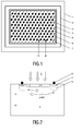
- FIG. 1 shows a pixel 1 of such a semiconductor component, a large number of such pixels being able to be arranged next to and below one another in order to fill a detector area of typically several square centimeters.
- the individual pixel 1 sblbst has an edge length of the order of 1 mm, that is to say an area of approximately 1 mm 2 .
- the pixel area is covered by a p-contact 2 as well a guard ring 3 framed.
- the guard ring is a linear one pn transition, which is characterized in particular by a deep n-well (i.e. diffused in) Doping can be formed in the p-doped path region 9 (FIG. 2).
- the guard ring 3 can be placed on a counter voltage during operation to the blocking function actively support.
- the guard ring 3 prevents that in the pixel area Light carriers generated by diffusion leave the area of the pixel and into can diffuse the area of an adjacent pixel.
- the guard ring thus ensures suppression of crosstalk (blurr) and thus for a clean separation of the Pixel.
- the active pixel area in which incident light quanta are detected is shown in the Essentially formed by the area within the guard ring.
- the pixel area is thereby formed from a p-doped path region 9, onto which (n +) -doped dot zones 7
- the dot zones 7 are in a hexagonal arrangement over the surface. This hexagonal arrangement ensures for a given number of dot zones 7, which are the capacitance of the component (Pixels) determines the greatest possible sensitivity.
- the dot zones 7 are connected to one another by metallic lines 6 which are inclined parallel to the pixel edges at 60 °, the lines 6 being electrically connected in the edge region of the pixel area by a peripheral collecting line 4.
- the charge carriers accumulated in the dot zones 7 can thus be skimmed off via the collecting line 4 and evaluated in evaluation electronics (not shown).
- the evaluation electronics can be accommodated in particular in the areas between two pixels.
- the dot zones with a greater density can be arranged in the edge region of the pixel, that is to say in the vicinity of the guard ring 4. In FIG. 1 there are five additional dot zones on the right edge of the pixel area recognizable, the placement of which differs from the otherwise predominant hexagonal arrangement pattern.
- FIG. 2 shows a cross section through the semiconductor component according to FIG. 1, which runs along the line II-II perpendicular to the surface and two neighboring dot zones 7 recorded.
- the semiconductor is constructed on a p-doped silicon substrate 10 in accordance with customary CMOS technology.
- a p-doped epitaxial layer 9 which is referred to in the present case as a railway region.
- the web region 9 is lightly doped, for example with a doping strength of 10 14 / cm 3 .
- Light quanta of wavelength ⁇ impinging on the semiconductor component from outside can penetrate as far as the path region 9 and generate pairs of charge carriers there.
- the mean distance traveled is referred to as the diffusion length L of the minority charge carriers and is typically of the order of 100 ⁇ m.
- 9 dot zones 7 are arranged on the surface of the web area.
- the dot zones 7 are produced by an n + doping (preferably by diffusion) in the web region 9, the doping strength typically being 10 16 / cm 3 .
- the barrier layer or depletion zone 8 of a semiconductor diode is formed in a known manner, which is further enlarged by polarity in the reverse direction.
- the metallic line contacts 6 are located on the dot zones 7 and electrically connect all the dot zones to one another in the manner shown in FIG.
- the dot zones 7 only occupy a very small area of typically 2 ⁇ m 2 , they collect charge carriers from a laterally wide area of the railway area 9 through the diffusion process. This means that the capacitance of the semiconductor component, which is determined by the total area of the dot Zones 7 of the pixel 1 is determined, can be kept small and yet light detection is possible from the entire pixel area.
- the hexagonal arrangement of the dot zones 7 ensures that the minority charge carriers after a minimal diffusion distance, a dot zone 7 or the associated one Reach barrier layer 8, so that a good compromise between the spacing of the dot zones 7 and sensitivity of the component is achieved. Furthermore, the distance between the dot zones 7 set the bandwidth of the sensor.
- the use of the hexagonal structure allows the bandwidth to be increased compared to all other conceivable ones Arrangements.
- FIG 2 it can also be seen that on the surface of the web area 9 between the dot zones 7 a (p +) - doped layer 5 is provided.
- This layer 5 is a (flat) threshold voltage implant manufactured as standard in CMOS technology to suppress the weak inversion to isolate the dot zones 7 am Si-SiO interface. Due to the different doping strength in the threshold voltage implantation 5 and in the railway area 9 arise electrical fields, which are advantageous to the Impact movement of minority carriers. That means that the charge carriers pass through these fields are preferably pushed laterally towards the dot zones 7.
Landscapes
- Solid State Image Pick-Up Elements (AREA)
- Light Receiving Elements (AREA)
Abstract
Description
Die Dot-Zonen einer Gruppe (Pixel) werden vorzugsweise so angeordnet, dass sie ein etwa rechtwinkliges Gebiet ausfüllen, dessen Fläche ca. 0,5 bis 5 mm2, besonders bevorzugt ca. 1 mm2 beträgt. Derartige für optische Halbleiterbauelemente große Flächen werden insbesondere bei den Pixeln von Röntgendetektoren benötigt, um das in einem Szintillatorkristall erzeugte Licht möglichst vollständig zu erfassen. Mit Hilfe der vorliegenden Erfindung können dabei trotz der großen Fläche hinreichend kleine Kapazitäten der Halbleiterdiode sichergestellt werden, so dass eine empfindliche und mit geringem Rauschen auszulesende Detektoranordnung entsteht.
- Fig. 1
- eine Aufsicht auf ein Pixel eines erfindungsgemäßen lichtsensitiven Halbleiterbauelementes;
- Fig. 2
- einen Querschnitt durch den Halbleiter nach Figur 1 entlang der Linie II-II, welcher zwei Dot-Zonen erfasst.
Zur Definition und zur Optimierung der aktiven Fläche des Bauelementes können im Randbereich des Pixels, das heißt in der Nähe des Guardringes 4, die Dot-Zonen mit einer größeren Dichte angeordnet sein So sind in Figur 1 am rechten Rand der Pixelfläche fünf zusätzliche Dot-Zonen erkennbar, deren Platzierung vom ansonsten vorherrschenden hexagonalen Anordnungsmuster abweicht.
Wenn die im Bahngebiet 9 durch Lichteinfall erzeugten Minoritätsladungsträger durch Diffusion in die Verarmungszone 8 gelangen, werden sie von dem dort herrschenden elektrischen Feld erfasst und zur Dot-Zone 7 geleitet. Von dort können sie dann über die Kontakte 6 zu einer entsprechenden Auswertungselektronik abgeleitet werden, um als Nachweis für das Licht zu dienen. Obwohl die Dot-Zonen 7 nur eine sehr geringe Fläche von typischerweise 2 µm2 einnehmen, sammeln sie durch den Diffusionsprozess Ladungsträger aus einem lateral weit ausgedehnten Bereich des Bahngebietes 9. Das bedeutet, dass die Kapazität des Halbleiterbauelementes, die durch die Gesamtfläche der Dot-Zonen 7 des Pixels 1 bestimmt wird, klein gehalten werden kann und dennoch aus der gesamten Pixelfläche ein Lichtnachweis möglich ist.
Claims (15)
- Lichtsensitives Halbleiterbauelement, enthaltend ein Bahngebiet (9) einer ersten Dotierung und damit in Kontakt stehende Dot-Zonen (7) entgegengesetzter Dotierung, wobei im Kontaktbereich des Bahngebietes mit jeder Dot-Zone ein pn-Übergang entsteht,
und wobei mindestens eine Gruppe von Dot-Zonen, die elektrisch parallel miteinander verschaltet sind, vorhanden ist. - Halbleiterbauelement nach Anspruch 1,
dadurch gekennzeichnet, dass die Dot-Zonen (7) der Gruppe zusammenhängend angeordnet sind - Halbleiterbauelement nach Anspruch 1 oder 2,
dadurch gekennzeichnet, dass die Dot-Zonen (7) der Gruppe in einer hexagonalen Verteilung auf dem Bahngebiet angeordnet sind - Halbleiterbauelement nach mindestens einem der Ansprüche 1 bis 3,
dadurch gekennzeichnet, dass die Dot-Zonen (7) über mindestens zwei Strompfade (6) an einer Sammelleitung (4) angeschlossen sind - Halbleiterbauelement nach mindestens einem der Ansprüche 1 bis 4,
dadurch gekennzeichnet, dass die Dot-Zonen (7) einer Gruppe von einem umlaufenden Guardring (3) umgeben werden, welcher als entgegengesetzte und vorzugsweise tiefgehende Dotierung im Bahngebiet (9) ausgebildet ist. - Halbleiterbauelement nach Anspruch 5,
dadurch gekennzeichnet, dass die Dot-Zonen (7) in Nachbarschaft zum Guardring (3) verdichtet angeordnet sind. - Halbleiterbauelement nach mindestens einem der Ansprüche 1 bis 6,
dadurch gekennzeichnet, dass die Oberfläche des Bahngebietes (9) zwischen den Dot-Zonen (7) eine Schwellspannungsimplantation (5) aufweist. - Halbleiterbauelement nach mindestens einem der Ansprüche 1 bis 7,
dadurch gekennzeichnet, dass das Bahngebiet (9) p-dotiert und die Dot-Zonen (7) n-dotiert sind oder umgekehrt. - Halbleiterbauelement nach mindestens einem der Ansprüche 1 bis 8,
dadurch gekennzeichnet, dass das Bahngebiet (9) so hergestellt ist, so dass Minoritätsladungsträger eine möglichst große Diffusionslänge (L) erreichen, vorzugsweise eine Diffusionslänge (L) von 50 bis 200 µm. - Halbleiterbauelement nach mindestens einem der Ansprüche 1 bis 9,
dadurch gekennzeichnet, dass der Abstand benachbarter Dot-Zonen (7) 10 bis 200 % der Diffusionslänge (L) der Minoritätsladungsträger im Bahngebiet (9) beträgt. - Halbleiterbauelement nach mindestens einem der Ansprüche 1 bis 10,
dadurch gekennzeichnet, dass die Fläche der Dot-Zonen (7) eine prozessabhängig minimale Strukturgröße aufweist, die vorzugsweise etwa 1 bis 5 µm2 beträgt. - Halbleiterbauelement nach mindestens einem der Ansprüche 1 bis 11,
dadurch gekennzeichnet, dass die Dot-Zonen (7) einer Gruppe ein etwa rechtwinkliges Gebiet (1) ausfüllen, dessen Fläche etwa 0,5 bis 5 mm2, vorzugsweise etwa 1 mm2 beträgt. - Halbleiterbauelement nach mindestens einem der Ansprüche 1 bis 12,
dadurch gekennzeichnet, dass es in CMOS-Technologie hergestellt ist. - Röntgendetektor mit einem lichtsensitiven Halbleiterbauelement, enthaltend ein Bahngebiet (9) einer ersten Dotierung und damit in Kontakt stehende Dot-Zonen (7) entgegengesetzter Dotierung, wobei im Kontaktbereich des Bahngebietes mit jeder Dot-Zone ein pn-Übergang entsteht,
und wobei mindestens eine Gruppe von Dot-Zonen, die elektrisch parallel miteinander verschaltet sind, vorhanden ist. - Röntgenuntersuchungsgerät mit einem Röntgendetektor mit einem lichtsensitiven Halbleiterbauelement, enthaltend ein Bahngebiet (9) einer ersten Dotierung und damit in Kontakt stehende Dot-Zonen (7) entgegengesetzter Dotierung, wobei im Kontaktbereich des Bahngebietes mit jeder Dot-Zone ein pn-Übergang entsteht,
und wobei mindestens eine Gruppe von Dot-Zonen, die elektrisch parallel miteinander verschaltet sind, vorhanden ist.
Applications Claiming Priority (2)
| Application Number | Priority Date | Filing Date | Title |
|---|---|---|---|
| DE10112374 | 2001-03-15 | ||
| DE10112374 | 2001-03-15 |
Publications (3)
| Publication Number | Publication Date |
|---|---|
| EP1241710A2 true EP1241710A2 (de) | 2002-09-18 |
| EP1241710A3 EP1241710A3 (de) | 2006-01-18 |
| EP1241710B1 EP1241710B1 (de) | 2009-09-09 |
Family
ID=7677504
Family Applications (1)
| Application Number | Title | Priority Date | Filing Date |
|---|---|---|---|
| EP02100255A Expired - Lifetime EP1241710B1 (de) | 2001-03-15 | 2002-03-14 | Lichtsensitives Halbleiterbauelement |
Country Status (4)
| Country | Link |
|---|---|
| US (1) | US6597025B2 (de) |
| EP (1) | EP1241710B1 (de) |
| JP (1) | JP2002324908A (de) |
| DE (1) | DE50213828D1 (de) |
Cited By (3)
| Publication number | Priority date | Publication date | Assignee | Title |
|---|---|---|---|---|
| WO2008050231A3 (en) * | 2006-10-23 | 2008-09-04 | Melexis Nv | Cmos photodiode for integration in an optical receiver |
| WO2011117161A3 (de) * | 2010-03-26 | 2012-02-23 | Iee International Electronics & Engineering S.A. | Lichtsensor mit photoempfindlicher halbleiterstruktur |
| EP3331034A1 (de) * | 2016-12-05 | 2018-06-06 | ams International AG | Strahlungsfestes schnelles photodiodenelement |
Families Citing this family (24)
| Publication number | Priority date | Publication date | Assignee | Title |
|---|---|---|---|---|
| US7057256B2 (en) | 2001-05-25 | 2006-06-06 | President & Fellows Of Harvard College | Silicon-based visible and near-infrared optoelectric devices |
| US7442629B2 (en) | 2004-09-24 | 2008-10-28 | President & Fellows Of Harvard College | Femtosecond laser-induced formation of submicrometer spikes on a semiconductor substrate |
| US7288825B2 (en) * | 2002-12-18 | 2007-10-30 | Noble Peak Vision Corp. | Low-noise semiconductor photodetectors |
| US6928144B2 (en) * | 2003-08-01 | 2005-08-09 | General Electric Company | Guard ring for direct photo-to-electron conversion detector array |
| DE60331060D1 (de) * | 2003-09-02 | 2010-03-11 | Univ Bruxelles | Ein durch einen Strom aus Majoritätsträgern unterstützter Detektor für elektromagnetische Strahlung |
| WO2006064399A2 (en) * | 2004-12-14 | 2006-06-22 | Koninklijke Philips Electronics, N.V. | Integrated pulse oximetry sensor |
| US7564083B2 (en) * | 2005-02-25 | 2009-07-21 | United Microelectronics Corp. | Active pixel sensor |
| CN101401208A (zh) * | 2006-03-15 | 2009-04-01 | 皇家飞利浦电子股份有限公司 | 用于辐射检测的半导体器件 |
| JP4391497B2 (ja) * | 2006-05-19 | 2009-12-24 | シャープ株式会社 | カラーセンサー、カラーセンサーの製造方法、センサー、及び電子機器 |
| US8212327B2 (en) * | 2008-03-06 | 2012-07-03 | Sionyx, Inc. | High fill-factor laser-treated semiconductor device on bulk material with single side contact scheme |
| JP5271104B2 (ja) * | 2009-02-13 | 2013-08-21 | 浜松ホトニクス株式会社 | リニアイメージセンサ |
| JP5091886B2 (ja) | 2009-02-13 | 2012-12-05 | 浜松ホトニクス株式会社 | イメージセンサ |
| US9673243B2 (en) | 2009-09-17 | 2017-06-06 | Sionyx, Llc | Photosensitive imaging devices and associated methods |
| US9911781B2 (en) | 2009-09-17 | 2018-03-06 | Sionyx, Llc | Photosensitive imaging devices and associated methods |
| US8692198B2 (en) | 2010-04-21 | 2014-04-08 | Sionyx, Inc. | Photosensitive imaging devices and associated methods |
| WO2011160130A2 (en) | 2010-06-18 | 2011-12-22 | Sionyx, Inc | High speed photosensitive devices and associated methods |
| US9496308B2 (en) | 2011-06-09 | 2016-11-15 | Sionyx, Llc | Process module for increasing the response of backside illuminated photosensitive imagers and associated methods |
| US20130016203A1 (en) | 2011-07-13 | 2013-01-17 | Saylor Stephen D | Biometric imaging devices and associated methods |
| US9064764B2 (en) | 2012-03-22 | 2015-06-23 | Sionyx, Inc. | Pixel isolation elements, devices, and associated methods |
| JP6466346B2 (ja) | 2013-02-15 | 2019-02-06 | サイオニクス、エルエルシー | アンチブルーミング特性を有するハイダイナミックレンジcmos画像センサおよび関連づけられた方法 |
| WO2014151093A1 (en) | 2013-03-15 | 2014-09-25 | Sionyx, Inc. | Three dimensional imaging utilizing stacked imager devices and associated methods |
| WO2014209421A1 (en) | 2013-06-29 | 2014-12-31 | Sionyx, Inc. | Shallow trench textured regions and associated methods |
| US9526468B2 (en) | 2014-09-09 | 2016-12-27 | General Electric Company | Multiple frame acquisition for exposure control in X-ray medical imagers |
| US20240105740A1 (en) * | 2020-12-11 | 2024-03-28 | Ams-Osram Ag | Photodiode device with enhanced characteristics |
Family Cites Families (11)
| Publication number | Priority date | Publication date | Assignee | Title |
|---|---|---|---|---|
| US3668473A (en) * | 1969-06-24 | 1972-06-06 | Tokyo Shibaura Electric Co | Photosensitive semi-conductor device |
| CA1177148A (en) * | 1981-10-06 | 1984-10-30 | Robert J. Mcintyre | Avalanche photodiode array |
| US5223919A (en) * | 1987-02-25 | 1993-06-29 | U. S. Philips Corp. | Photosensitive device suitable for high voltage operation |
| DE19638693C2 (de) * | 1996-09-20 | 1998-12-17 | Fraunhofer Ges Forschung | Photodetektor und Farbfilter unter Verwendung eines Photodetektors |
| EP0883187A1 (de) | 1997-06-04 | 1998-12-09 | Interuniversitair Micro-Elektronica Centrum Vzw | Detektor für elektromagnetische Strahlung, Pixelstruktur mit höher Empfindlichkeit mit Verwendung dieses Detektors und Verfahren zu dessen Herstellung |
| JP3413078B2 (ja) * | 1997-10-06 | 2003-06-03 | キヤノン株式会社 | 光電変換装置と密着型イメージセンサ |
| US6198118B1 (en) * | 1998-03-09 | 2001-03-06 | Integration Associates, Inc. | Distributed photodiode structure |
| US6034321A (en) * | 1998-03-24 | 2000-03-07 | Essential Research, Inc. | Dot-junction photovoltaic cells using high-absorption semiconductors |
| US6047042A (en) * | 1998-03-25 | 2000-04-04 | Continental X-Ray Corporation | Automatic exposure and brightness control for fluoroscopic and radio-graphic imaging |
| JP4011734B2 (ja) * | 1998-06-02 | 2007-11-21 | キヤノン株式会社 | 2次元光センサ、それを用いた放射線検出装置及び放射線診断システム |
| US6252218B1 (en) * | 1999-02-02 | 2001-06-26 | Agilent Technologies, Inc | Amorphous silicon active pixel sensor with rectangular readout layer in a hexagonal grid layout |
-
2002
- 2002-03-12 US US10/095,832 patent/US6597025B2/en not_active Expired - Lifetime
- 2002-03-14 EP EP02100255A patent/EP1241710B1/de not_active Expired - Lifetime
- 2002-03-14 JP JP2002070448A patent/JP2002324908A/ja not_active Ceased
- 2002-03-14 DE DE50213828T patent/DE50213828D1/de not_active Expired - Lifetime
Cited By (5)
| Publication number | Priority date | Publication date | Assignee | Title |
|---|---|---|---|---|
| WO2008050231A3 (en) * | 2006-10-23 | 2008-09-04 | Melexis Nv | Cmos photodiode for integration in an optical receiver |
| WO2011117161A3 (de) * | 2010-03-26 | 2012-02-23 | Iee International Electronics & Engineering S.A. | Lichtsensor mit photoempfindlicher halbleiterstruktur |
| EP3331034A1 (de) * | 2016-12-05 | 2018-06-06 | ams International AG | Strahlungsfestes schnelles photodiodenelement |
| WO2018104111A1 (en) * | 2016-12-05 | 2018-06-14 | Ams International Ag | Radiation-hard high-speed photodiode device |
| US10985291B2 (en) | 2016-12-05 | 2021-04-20 | Ams International Ag | Radiation-hard high-speed photodiode device |
Also Published As
| Publication number | Publication date |
|---|---|
| US6597025B2 (en) | 2003-07-22 |
| DE50213828D1 (de) | 2009-10-22 |
| EP1241710A3 (de) | 2006-01-18 |
| JP2002324908A (ja) | 2002-11-08 |
| US20020140045A1 (en) | 2002-10-03 |
| EP1241710B1 (de) | 2009-09-09 |
Similar Documents
| Publication | Publication Date | Title |
|---|---|---|
| EP1241710B1 (de) | Lichtsensitives Halbleiterbauelement | |
| DE102009020218B3 (de) | Detektor und Verfahren zum Detektieren elektromagnetischer Strahlung und Computerprogramm zur Durchführung des Verfahrens | |
| DE102007037020B3 (de) | Avalanche-Photodiode | |
| DE2849511A1 (de) | Photodetektor-anordnung | |
| WO2020201189A1 (de) | Avalanche-photodioden-array | |
| EP1431779A1 (de) | Halbleiter-Detektor mit optimiertem Strahlungseintrittsfenster | |
| EP2549536B1 (de) | Halbleiterstruktur zur Photonendetektion | |
| DE10251735B4 (de) | Aktives Pixel und Verfahren zur Herstellung eines aktiven Pixels | |
| WO2010057835A2 (de) | Strahlungsdetektor, verwendung eines strahlungsdetektors und verfahren zur herstellung eines strahlungsdetektors | |
| DE2922250C2 (de) | ||
| DE3637817A1 (de) | Hochempfindliche photodiode | |
| DE102022126443B4 (de) | Avalanche photodetektoren mit einer multi-dicken-ladungsschicht | |
| AT392704B (de) | Strahlungsempfindliche halbleiteranordnung | |
| EP0902982B1 (de) | Streifendetektor | |
| DE112013005690B4 (de) | Fotodiodenanordnung | |
| DE112021006393T5 (de) | Fotodiodenvorrichtung mit verbesserten Eigenschaften | |
| DE2713876A1 (de) | Ladungsgekoppeltes element (ccd) | |
| DE102012101151A1 (de) | Halbleiter MOS Eingangsfenster für Strahlungsdetektoren | |
| DE3878339T2 (de) | Detektor fuer ionisierende teilchen. | |
| DE1957335C3 (de) | Strahlungsempfindliches Halbleiterbauelement und seine Verwendung in einer Bildaufnahmeröhre | |
| EP1807876B1 (de) | Vertikale pin oder nip fotodiode und verfahren zur herstellung, kompatibel zu einem konventionellen cmos-prozess | |
| EP1208598B1 (de) | Bildzelle, bildsensor und herstellungsverfahren hierfür | |
| DE112021004929B4 (de) | Fotosensorzelle, fotosensor und verfahren | |
| DE102010019993A1 (de) | Fotodiode mit Polarisator | |
| DE69935371T2 (de) | Halbleiterphotodetektor mit erhöhter lichtempfänglicher Oberfläche und Hochgeschwindigkeitsleistung |
Legal Events
| Date | Code | Title | Description |
|---|---|---|---|
| PUAI | Public reference made under article 153(3) epc to a published international application that has entered the european phase |
Free format text: ORIGINAL CODE: 0009012 |
|
| AK | Designated contracting states |
Kind code of ref document: A2 Designated state(s): AT BE CH CY DE DK ES FI FR GB GR IE IT LI LU MC NL PT SE TR |
|
| AX | Request for extension of the european patent |
Free format text: AL;LT;LV;MK;RO;SI |
|
| RAP1 | Party data changed (applicant data changed or rights of an application transferred) |
Owner name: KONINKLIJKE PHILIPS ELECTRONICS N.V. Owner name: PHILIPS CORPORATE INTELLECTUAL PROPERTY GMBH |
|
| RAP1 | Party data changed (applicant data changed or rights of an application transferred) |
Owner name: PHILIPS INTELLECTUAL PROPERTY & STANDARDS GMBH Owner name: KONINKLIJKE PHILIPS ELECTRONICS N.V. |
|
| RAP1 | Party data changed (applicant data changed or rights of an application transferred) |
Owner name: FRAUNHOFER-GESELLSCHAFT ZUR FOERDERUNG DERANGEWAND Owner name: PHILIPS INTELLECTUAL PROPERTY & STANDARDS GMBH Owner name: KONINKLIJKE PHILIPS ELECTRONICS N.V. |
|
| RAP1 | Party data changed (applicant data changed or rights of an application transferred) |
Owner name: PHILIPS INTELLECTUAL PROPERTY & STANDARDS GMBH Owner name: KONINKLIJKE PHILIPS ELECTRONICS N.V. Owner name: FRAUNHOFER-GESELLSCHAFT ZUR FOERDERUNG DERANGEWAND |
|
| RIN1 | Information on inventor provided before grant (corrected) |
Inventor name: BROCKHERDE, WERNER Inventor name: LAUTER, JOSEFC/O PHILIPS CORPORATE Inventor name: HAUSSCHILD, RALF, DR. Inventor name: KEMNA, ARMIN |
|
| RIN1 | Information on inventor provided before grant (corrected) |
Inventor name: HAUSSCHILD, RALF, DR. Inventor name: KEMNA, ARMIN Inventor name: LAUTER, JOSEFC/O PHILIPS CORPORATE Inventor name: BROCKHERDE, WERNER |
|
| PUAL | Search report despatched |
Free format text: ORIGINAL CODE: 0009013 |
|
| AK | Designated contracting states |
Kind code of ref document: A3 Designated state(s): AT BE CH CY DE DK ES FI FR GB GR IE IT LI LU MC NL PT SE TR |
|
| AX | Request for extension of the european patent |
Extension state: AL LT LV MK RO SI |
|
| RIC1 | Information provided on ipc code assigned before grant |
Ipc: H01L 31/0352 20060101AFI20020704BHEP Ipc: H01L 27/146 20060101ALI20051125BHEP Ipc: H01L 31/103 20060101ALI20051125BHEP |
|
| 17P | Request for examination filed |
Effective date: 20060718 |
|
| AKX | Designation fees paid |
Designated state(s): DE FR GB |
|
| 17Q | First examination report despatched |
Effective date: 20060905 |
|
| RAP1 | Party data changed (applicant data changed or rights of an application transferred) |
Owner name: FRAUNHOFER-GESELLSCHAFT ZUR FOERDERUNG DER ANGEWAN Owner name: PHILIPS INTELLECTUAL PROPERTY & STANDARDS GMBH Owner name: KONINKLIJKE PHILIPS ELECTRONICS N.V. |
|
| RAP1 | Party data changed (applicant data changed or rights of an application transferred) |
Owner name: FRAUNHOFER-GESELLSCHAFT ZUR FOERDERUNG DER ANGEWAN Owner name: KONINKLIJKE PHILIPS ELECTRONICS N.V. Owner name: PHILIPS INTELLECTUAL PROPERTY & STANDARDS GMBH |
|
| GRAP | Despatch of communication of intention to grant a patent |
Free format text: ORIGINAL CODE: EPIDOSNIGR1 |
|
| GRAS | Grant fee paid |
Free format text: ORIGINAL CODE: EPIDOSNIGR3 |
|
| GRAA | (expected) grant |
Free format text: ORIGINAL CODE: 0009210 |
|
| AK | Designated contracting states |
Kind code of ref document: B1 Designated state(s): DE FR GB |
|
| REG | Reference to a national code |
Ref country code: GB Ref legal event code: FG4D Free format text: NOT ENGLISH |
|
| REF | Corresponds to: |
Ref document number: 50213828 Country of ref document: DE Date of ref document: 20091022 Kind code of ref document: P |
|
| PLBE | No opposition filed within time limit |
Free format text: ORIGINAL CODE: 0009261 |
|
| STAA | Information on the status of an ep patent application or granted ep patent |
Free format text: STATUS: NO OPPOSITION FILED WITHIN TIME LIMIT |
|
| 26N | No opposition filed |
Effective date: 20100610 |
|
| GBPC | Gb: european patent ceased through non-payment of renewal fee |
Effective date: 20100314 |
|
| PG25 | Lapsed in a contracting state [announced via postgrant information from national office to epo] |
Ref country code: GB Free format text: LAPSE BECAUSE OF NON-PAYMENT OF DUE FEES Effective date: 20100314 |
|
| REG | Reference to a national code |
Ref country code: DE Ref legal event code: R081 Ref document number: 50213828 Country of ref document: DE Owner name: PHILIPS GMBH, DE Free format text: FORMER OWNER: PHILIPS INTELLECTUAL PROPERTY & STANDARDS GMBH, 20099 HAMBURG, DE Effective date: 20140327 Ref country code: DE Ref legal event code: R081 Ref document number: 50213828 Country of ref document: DE Owner name: PHILIPS DEUTSCHLAND GMBH, DE Free format text: FORMER OWNER: PHILIPS INTELLECTUAL PROPERTY & STANDARDS GMBH, 20099 HAMBURG, DE Effective date: 20140327 |
|
| REG | Reference to a national code |
Ref country code: FR Ref legal event code: CD Owner name: KONINKLIJKE PHILIPS ELECTRONICS N Effective date: 20140806 Ref country code: FR Ref legal event code: CA Effective date: 20140806 Ref country code: FR Ref legal event code: CD Owner name: FRAUNHOFER-GESELLSCHAFT ZURFORDERUNG DER ANGEW, DE Effective date: 20140806 Ref country code: FR Ref legal event code: CD Owner name: PHILIPS INTELLECTUAL PROPERTY & STANDARDS GMBH, DE Effective date: 20140806 |
|
| REG | Reference to a national code |
Ref country code: DE Ref legal event code: R082 Ref document number: 50213828 Country of ref document: DE Representative=s name: MEISSNER, BOLTE & PARTNER GBR, DE Ref country code: DE Ref legal event code: R081 Ref document number: 50213828 Country of ref document: DE Owner name: PHILIPS GMBH, DE Free format text: FORMER OWNER: PHILIPS DEUTSCHLAND GMBH, 20099 HAMBURG, DE Ref country code: DE Ref legal event code: R082 Ref document number: 50213828 Country of ref document: DE Representative=s name: MEISSNER BOLTE PATENTANWAELTE RECHTSANWAELTE P, DE |
|
| REG | Reference to a national code |
Ref country code: FR Ref legal event code: PLFP Year of fee payment: 15 |
|
| REG | Reference to a national code |
Ref country code: FR Ref legal event code: PLFP Year of fee payment: 16 |
|
| REG | Reference to a national code |
Ref country code: FR Ref legal event code: PLFP Year of fee payment: 17 |
|
| PGFP | Annual fee paid to national office [announced via postgrant information from national office to epo] |
Ref country code: FR Payment date: 20190328 Year of fee payment: 18 |
|
| PGFP | Annual fee paid to national office [announced via postgrant information from national office to epo] |
Ref country code: DE Payment date: 20190528 Year of fee payment: 18 |
|
| REG | Reference to a national code |
Ref country code: DE Ref legal event code: R119 Ref document number: 50213828 Country of ref document: DE |
|
| PG25 | Lapsed in a contracting state [announced via postgrant information from national office to epo] |
Ref country code: DE Free format text: LAPSE BECAUSE OF NON-PAYMENT OF DUE FEES Effective date: 20201001 Ref country code: FR Free format text: LAPSE BECAUSE OF NON-PAYMENT OF DUE FEES Effective date: 20200331 |