EP1237395B1 - Leiterplattenanordnung - Google Patents
Leiterplattenanordnung Download PDFInfo
- Publication number
- EP1237395B1 EP1237395B1 EP01130331A EP01130331A EP1237395B1 EP 1237395 B1 EP1237395 B1 EP 1237395B1 EP 01130331 A EP01130331 A EP 01130331A EP 01130331 A EP01130331 A EP 01130331A EP 1237395 B1 EP1237395 B1 EP 1237395B1
- Authority
- EP
- European Patent Office
- Prior art keywords
- circuit board
- printed circuit
- slots
- standard
- boards
- Prior art date
- Legal status (The legal status is an assumption and is not a legal conclusion. Google has not performed a legal analysis and makes no representation as to the accuracy of the status listed.)
- Expired - Lifetime
Links
Images
Classifications
-
- G—PHYSICS
- G06—COMPUTING OR CALCULATING; COUNTING
- G06F—ELECTRIC DIGITAL DATA PROCESSING
- G06F1/00—Details not covered by groups G06F3/00 - G06F13/00 and G06F21/00
- G06F1/16—Constructional details or arrangements
- G06F1/18—Packaging or power distribution
- G06F1/183—Internal mounting support structures, e.g. for supporting printed circuit boards
- G06F1/185—Mounting of expansion boards
-
- G—PHYSICS
- G06—COMPUTING OR CALCULATING; COUNTING
- G06F—ELECTRIC DIGITAL DATA PROCESSING
- G06F1/00—Details not covered by groups G06F3/00 - G06F13/00 and G06F21/00
- G06F1/16—Constructional details or arrangements
- G06F1/18—Packaging or power distribution
- G06F1/183—Internal mounting support structures, e.g. for supporting printed circuit boards
- G06F1/184—Mounting of motherboards
-
- G—PHYSICS
- G06—COMPUTING OR CALCULATING; COUNTING
- G06F—ELECTRIC DIGITAL DATA PROCESSING
- G06F1/00—Details not covered by groups G06F3/00 - G06F13/00 and G06F21/00
- G06F1/16—Constructional details or arrangements
- G06F1/18—Packaging or power distribution
- G06F1/183—Internal mounting support structures, e.g. for supporting printed circuit boards
- G06F1/185—Mounting of expansion boards
- G06F1/186—Securing of expansion boards in correspondence to slots provided at the computer enclosure
-
- H—ELECTRICITY
- H05—ELECTRIC TECHNIQUES NOT OTHERWISE PROVIDED FOR
- H05K—PRINTED CIRCUITS; CASINGS OR CONSTRUCTIONAL DETAILS OF ELECTRIC APPARATUS; MANUFACTURE OF ASSEMBLAGES OF ELECTRICAL COMPONENTS
- H05K1/00—Printed circuits
- H05K1/02—Details
- H05K1/14—Structural association of two or more printed circuits
- H05K1/142—Arrangements of planar printed circuit boards in the same plane, e.g. auxiliary printed circuit insert mounted in a main printed circuit
Definitions
- the invention relates to a printed circuit board assembly having a first printed circuit board with first predetermined dimensions and a second printed circuit board, which is connectable by means of a connector to the first printed circuit board.
- a circuit board assembly according to the preamble of claim 1 is made US-A-6046912 known.
- riser cards Such printed circuit board assemblies are known from the prior art as so-called riser cards. These are used for the purpose of providing additional slots.
- a riser card is inserted vertically into a so-called PCI slot.
- the printed circuit boards inserted on the riser card, so-called expansion cards, are then parallel to the first printed circuit board. Thus, they are in an area in which the spatial arrangement can collide with other components arranged on the printed circuit board.
- Another problem is the connection to the bus system of the mainboard, since PCT slots are not actually intended for the connection and control of multiple expansion cards.
- motherboards which have more slots for expansion cards.
- motherboards which have more slots for expansion cards.
- two different types of motherboard are developed, manufactured and stored, which causes additional costs.
- the object of the invention is therefore to provide a printed circuit board assembly which allows a simple extension of the first circuit board to further components, in particular slots.
- a second circuit board is connected via a connector to the first circuit board, wherein both the size of the first circuit board and the size of the arrangement of the first and the second circuit board specified dimensions correspond.
- This is the case, for example, with mainboards for data processing systems, where various standards have been established.
- One of the standards concerns so-called ATX boards and the corresponding second standard is called ⁇ ATX.
- the size of the ATX boards is 244 mm x 305 mm, while the size of ⁇ ATX boards is 244 mm x 244 mm.
- the storage is complicated, since both circuit boards must be stored.
- the development of two different boards is very expensive, although they have the same or largely the same functionalities.
- the arrangement according to the invention proves to be particularly advantageous when all important components are located on the first printed circuit board and the second printed circuit board only has plug-in devices for receiving plug-in cards.
- the complex development steps relate only to the first circuit board, so that this effort for different sizes of printed circuit boards consisting of the first and second circuit board or even the first circuit board must be made only once.
- the plug-in cards or an interconnection of the connections for continuation on the plug connection are necessary, this is relatively simple from a design point of view.
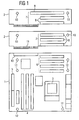
- the first circuit board 1 is the mainboard of a data processing device and has a CPU 3, memory components 4, connectors 5 and slots 6 for expansion cards.
- the length and width of the circuit board 1 is fixed. It is determined by standardization or quasi-standards, to which inter alia, the housing size, etc. are tuned. Also matched, for example, the positioning of the holes 12 for mounting screws.
- the circuit board 1 is a motherboard according to the ⁇ ATX standard, which has a size of 244 mm x 244 mm.
- the invention provides that the dimensions of the second printed circuit boards are designed so that the arrangement of the first and second printed circuit boards 1 and 2 second fixed dimensions, namely according to the ATX standard, having.
- Bolt holes 13 for mounting screws are ideally provided on the second circuit board 2 so that they also correspond to the position for holes according to the ATX standard.
- a standard housing for ATX boards and all the corresponding standard components can be used.
- the printed circuit board 2 in FIG. 1 is equipped with three PCI slots 8. Between a connector 11 for connection to the first circuit board 1 and the PCI slots 8, of course, strip conductors are provided according to the prescribed connection of the slots 8. To the clarity of FIG. 1 to maintain, the conductor connections are not shown.
- a second printed circuit board 12 can be used, which in the case shown has two PCI slots 8 and one ISA slot 9.
- Such a second circuit board 12 can be usefully used when an ISA slot 9 is required by the user of the circuit board assembly, although this is no longer provided in modern motherboards.
- An ISA slot 9 is necessary if older plug-in cards in a new data processing device should be used, but the manufacturer can not provide a PCI version of the plug-in card.
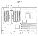
- FIG. 2 the circuit board assembly of the first circuit board 1 and the second circuit board 2 is shown in more detail.
- the connector 10 on the first circuit board 1 for connecting the second circuit board 2 is provided only when an extension of the first circuit board 1 with the second circuit board 2 according to the invention is actually provided. Otherwise, in the course of a uniform printed circuit board design, only the connections for the connector 10 are provided. An equipping but not done, so that costs can be saved at this point.
- the connectors 10 and 11 are made mechanically solid, so that even with a mechanical load by plugging expansion cards into slots of the second circuit board 2, a reliable electrical connection can be ensured.
- a certain problem is the mechanical stability of the second circuit board 2, since the mechanical forces can be absorbed by the insertion of expansion cards in the slots 7 of the second circuit board of only two support points in the mounting screws in the holes 13. Therefore, the voltage supply of the second printed circuit board 2 is advantageously performed by connectors 17 and 18 also mechanically solid and also arranged on the other side of the connecting region between the first and the second circuit board 1 and 2.
- the figure 4 shows the special PCI connector strip 14 in a cross section, wherein it can be seen that the connector strip 14 is electrically connected to the circuit board 2, but mechanically also a connection to the first circuit board 1 is.
Landscapes
- Engineering & Computer Science (AREA)
- Theoretical Computer Science (AREA)
- General Engineering & Computer Science (AREA)
- Computer Hardware Design (AREA)
- General Physics & Mathematics (AREA)
- Physics & Mathematics (AREA)
- Human Computer Interaction (AREA)
- Power Engineering (AREA)
- Microelectronics & Electronic Packaging (AREA)
- Combinations Of Printed Boards (AREA)
- Coupling Device And Connection With Printed Circuit (AREA)
- Mounting Of Printed Circuit Boards And The Like (AREA)
- Paper (AREA)
- Manufacturing Of Electrical Connectors (AREA)
Description
- Die Erfindung betrifft eine Leiterplattenanordnung mit einer ersten Leiterplatte mit ersten festgelegten Abmessungen und einer zweiten Leiterplatte, die mittels eines Steckverbinders mit der ersten Leiterplatte verbindbar ist.
- Eine Leiterplattenanordnung nach dem Oberbegriff des Anspruchs 1 ist aus
US-A-6046912 bekannt. - Derartige Leiterplattenanordnungen sind aus dem Stand der Technik als sogenannte Riser-Karten bekannt. Diese werden zu dem Zweck eingesetzt, zusätzliche Steckplätze bereitzustellen. Eine Riser-Karte wird dabei senkrecht in einen sogenannten PCI-Steckplatz eingesteckt. Die auf die Riser-Card eingesteckten Leiterplatten, sogenannte Erweiterungskarten, liegen dann parallel zur ersten Leiterplatte. Damit befinden sie sich in einem Bereich, in dem die räumlich Anordnung mit anderen auf der Leiterplatte angeordneten Komponenten kollidieren kann. Problematisch ist auch die Anbindung an das Bussystem des Mainboards, da PCT-Steckplätze eigentlich nicht für die Anbindung und Kontrolle mehrerer Erweiterungskarten vorgesehen sind.
- Alternativ werden von vorne herein größere Leiterplatten als Mainboard vorgesehen, die mehr Steckplätze für Erweiterungskarten aufweisen. Um sowohl Systeme mit einer geringen Anzahl von Steckplätzen und kleinen Abmessungen als auch Systeme mit einer großen Anzahl von Steckplätzen und verhältnismäßig großen Abmessungen anbieten zu können, werden also zwei verschiedene Mainboardtypen entwickelt, hergestellt und gelagert, was zusätzliche Kosten verursacht.
- Aufgabe der Erfindung ist es daher, eine Leiterplattenanordnung anzugeben, die eine einfache Erweiterung der ersten Leiterplatte um weitere Komponenten, insbesondere Steckplätze, ermöglicht.
- Diese Aufgabe wird durch eine Anordnung der eingangs genannten Art gelöst, die dadurch gekennzeichnet ist, daß im verbundenen Zustand sich die erste und zweite Leiterplatte in einer Ebene befinden und die Abmessungen der zweiten Leiterplatte so bemessen sind, daß die Anordnung aus der ersten und der zweiten Leiterplatte zweite festgelegte Abmessungen aufweist.
- Gemäß der Erfindung wird also eine zweite Leiterplatte über einen Steckverbinder mit der ersten Leiterplatte verbunden, wobei sowohl die Größe der ersten Leiterplatte als auch die Größe der Anordnung aus der ersten und der zweiten Leiterplatte festgelegten Abmessungen entsprechen. Dies ist beispielsweise bei Mainboards für Datenverarbeitungsanlagen der Fall, wo sich verschiedene Standards etabliert haben. Einer der Standards betrifft sogenannte ATX-Boards und der entsprechende zweite Standard dazu wird als µATX bezeichnet. Die Größe der ATX-Boards beträgt 244 mm x 305 mm, während die Größe von µATX-Boards bei 244 mm x 244 mm liegt. Entsprechend gibt es Gehäuse, die für ATX-Boards und andere, die für µATX-Boards geeignet sind. Die Lagerhaltung ist aufwendig, da beide Leiterplatten bevorratet werden müssen. Zudem ist die Entwicklung von zwei verschiedenen Boards sehr aufwendig, obwohl sie gleiche bzw. weitgehend gleiche Funktionalitäten aufweisen.
- Besonders vorteilhaft erweist sich die erfindungsgemäße Anordnung, wenn sich sämtliche wichtigen Komponenten auf der ersten Leiterplatte befinden und die zweite Leiterplatte nur noch Steckvorrichtungen zur Aufnahme von Einsteckkarten aufweist. In diesem Fall betreffen die aufwendigen Entwicklungsschritte nur die erste Leiterplatte, so daß dieser Aufwand für verschiedene Größen von Leiterplatten bestehend aus der ersten und zweiten Leiterplatte oder auch nur der ersten Leiterplatte nur einmal geleistet werden muß. Auf der zweiten Leiterplatte sind nur die Steckkarten bzw. eine Verschaltung der Anschlüsse zur Weiterführung auf den Steckanschluß notwendig, wobei dies aus Entwurfsicht verhältnismäßig einfach ist.
- Die Erfindung wird nachfolgend anhand eines Ausführungsbeispiels näher erläutert. Es zeigt:
- Figur 1
- ein erstes Ausführungsbeispiel einer erfindungsgemäßen Leiterplattenanordnung,
- Figur 2
- eine detailliertere Darstellung des Ausführungsbeispiel von
Figur 1 , - Figur 3
- ein Detail eines PCI-Steckplatzes in einer Draufsicht und
- Figur 4
- den PCI-Steckplatz von
Figur 3 in einer Seitenansicht. - In der
Figur 1 ist in einer vereinfachten Darstellung die Anordnung mit zwei Leiterplatten 1 und 2 dargestellt. Alternativ zur zweiten Leiterplatte 2 kann auch eine Leiterplatte 12 vorgesehen werden. Die erste Leiterplatte 1 ist das Mainboard einer Datenverarbeitungseinrichtung und besitzt eine CPU 3, Speicherkomponenten 4, Anschlüsse 5 und Steckplätze 6 für Erweiterungskarten. Die Länge und Breite der Leiterplatte 1 ist festgelegt. Sie ist bestimmt durch Normung oder Quasi-Standards, auf die unter anderem die Gehäusegröße usw. abgestimmt sind. Ebenso abgestimmt sind beispielsweise die Positionierungen der Bohrungen 12 für Befestigungsschrauben. In diesem Fall handelt es sich bei der Leiterplatte 1 um ein Mainboard nach dem µATX-Standard, das eine Größe von 244 mm x 244 mm aufweist . - In vielen Fällen sind aber zusätzliche Steckplätze 7 für Erweiterungskarten gefragt, die auch ein größeres Gehäuse notwendig machen. Bisher wurde in diesem Fall ein anderes Mainboard verwendet, das die erforderlichen zusätzlichen Steckplätze aufweist. Die Größe eines solchen ATX-Boards beträgt 244 mmm x 305 mm. Die Bereitstellung dieser unterschiedlichen Mainboards verursacht erhebliche Kosten in der Entwicklung, Herstellung und Lagerung. Bei Verwendung einer Anordnung nach der Erfindung wird nur noch die erste Leiterplatte 1 nach dem µATX-Standard entwickelt und in den Fällen, in denen weitere Steckplätze 7 notwendig sind, die zweite Leiterplatte 2 als Erweiterungsleiterplatte zu der ersten Leiterplatte 1 durch eine Steckverbindung 10 und 11 mit dieser verbunden. Um für diese erweiterte Leiterplattenanordnung kein besonderes Gehäuse verwenden zu müssen, sieht die Erfindung vor, daß die Abmessungen der zweiten Leiterplatten so ausgelegt sind, daß die Anordnung aus der ersten und zweiten Leiterplatte 1 und 2 zweite festgelegte Abmessungen, nämlich gemäß dem ATX-Standard, aufweist. Bohrungen 13 für Befestigungsschrauben werden idealerweise auf der zweiten Leiterplatte 2 so vorgesehen, daß sie ebenfalls der Position für Bohrungen nach dem ATX-Standard entsprechen. Somit kann ein Standardgehäuse für ATX-Boards und alle entsprechenden Standardkomponenten verwendet werden.
- Die Leiterplatte 2 in
Figur 1 ist mit drei PCI-Steckplätzen 8 ausgerüstet. Zwischen einem Steckverbinder 11 zum Anschluß an die erste Leiterplatte 1 und den PCI-Steckplätzen 8 sind natürlich Leiterbahnen vorgesehen entsprechend dem vorgeschriebenen Anschluß der Steckplätze 8. Um die Übersichtlichkeit derFigur 1 zu wahren, sind die Leiterverbindungen nicht dargestellt. - Alternativ zu der zweiten Leiterplatte 2 kann eine zweite Leiterplatte 12 eingesetzt werden, die im gezeigten Fall zwei PCI-Steckplätze 8 und einen ISA-Steckplatz 9 besitzt. Eine solche zweite Leiterplatte 12 kann nutzbringend eingesetzt werden, wenn von dem Benutzer der Leiterplattenanordnung ein ISA-Steckplatz 9 gefordert ist, obwohl dies bei modernen Mainboards nicht mehr vorgesehen ist. Ein ISA-Steckplatz 9 ist notwendig, wenn ältere Steckkarten in einer neuen Datenverarbeitungsvorrichtung verwendet werden sollen, der Hersteller aber keine PCI-Version der Steckkarte bereitstellen kann.
- In der Darstellung von
Figur 2 ist die Leiterplattenanordnung aus der ersten Leiterplatte 1 und der zweiten Leiterplatte 2 detaillierter dargestellt. Der Steckverbinder 10 auf der ersten Leiterplatte 1 zum Anschluß der zweiten Leiterplatte 2 ist nur dann vorzusehen, wenn eine Erweiterung der ersten Leiterplatte 1 mit der zweiter Leiterplatte 2 gemäß der Erfindung auch tatsächlich vorgesehen ist. Ansonsten sind, im Zuge eines einheitlichen Leiterplattendesigns, lediglich die Anschlüsse für den Steckverbinder 10 vorgesehen. Eine Bestükkung erfolgt aber nicht, so daß an dieser Stelle Kosten eingespart werden können. Die Steckverbinder 10 und 11 sind mechanisch solide ausgeführt, damit auch bei einer mechanischen Belastung durch das Einstecken von Erweiterungskarten in Steckplätze der zweiten Leiterplatte 2 eine zuverlässige elektrische Verbindung sichergestellt werden kann. - Ein gewisses Problem stellt die mechanische Stabilität der zweiten Leiterplatte 2 dar, da die mechanisch einwirkenden Kräfte durch das Einstecken von Erweiterungskarten in die Steckplätze 7 der zweiten Leiterplatte von nur zwei Abstützpunkten bei den Befestigungsschrauben in den Bohrungen 13 aufgefangen werden können. Daher ist in vorteilhafter Weise die Spannungsversorgung der zweiten Leiterplatte 2 durch Steckverbinder 17 und 18 ebenfalls mechanisch solide ausgeführt und außerdem an der anderen Seite des Verbindungsbereichs zwischen der ersten und der zweiten Leiterplatte 1 und 2 angeordnet.
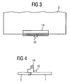
- Darüber hinaus ist für die Steckplätze 7 eine Anordnung vorgeschlagen, die es ermöglicht, trotz des Aneinandersetzens der zwei Leiterplatten einen Abstand der Steckplätze 6 bzw. 7 voneinander so zu gewährleisten, wie dies bei einem speziellen ATX-Board der Fall ist. Eine der PCI-Steckerleisten 14 erstreckt sich nämlich über die Kante der zweiten Leiterplatte 2 hinaus, um im zusammengesteckten Zustand auf der Oberfläche der ersten Leiterplatte 1 aufzuliegen. Dadurch findet eine mechanische Übertragung von Kräften, die auf die zweite Leiterplatte 2 wirken, auf die erste Leiterplatte 1 statt. Zudem ist eine Haltenase 15 vorgesehen, durch die in Verbindung mit entsprechenden Rastausnehmungen 16 durch Einrasten sichergestellt ist, daß die beiden Leiterplatten ordnungsgemäß miteinander verbunden und beispielsweise durch Verrutschen nicht wieder getrennt werden können.
- In der
Figur 3 ist diese spezielle PCI-Steckerleiste in einer Vergrößerung dargestellt. -
Die Figur 4 zeigt die spezielle PCI-Steckerleiste 14 in einem Querschnitt, wobei erkennbar ist, daß die Steckerleiste 14 elektrisch mit der Leiterplatte 2 verbunden ist, mechanisch aber auch eine Verbindung zur ersten Leiterplatte 1 besteht. - Trotz der erfindungsgemäßen Leiterplattenanordnung sind für die Logistik weiterhin zwei unterschiedliche Komponenten vorzusehen. Da die zweiten Leiterplatten 2 jedoch keine empfindlichen elektronischen Komponenten enthalten und darüber hinaus wesentlich kleiner sind als die ersten Leiterplatten 1, ergibt sich auch für die Logistik ein Kostenvorteil.
-
- 1
- erste Leiterplatte
- 2
- zweite Leiterplatte
- 3
- CPU
- 4
- Speicherbausteine
- 5
- Steckanschlüsse
- 6
- Steckplätze
- 7
- Steckplätze
- 8
- PCI-Steckplätze
- 9
- ISA-Steckplätze
- 10
- Steckverbinder
- 11
- Steckverbinder
- 12
- Bohrungen der ersten Leiterplatte
- 13
- Bohrungen der zweiten Leiterplatte
- 14
- Spezial-PCI-Steckerleiste
- 15
- Rastnase
- 16
- Rastausnehmung
- 17
- Steckverbinder
- 18
- Steckverbinder
- 19
- zweite Leiterplatte
Claims (2)
- Leiterplattenanordnung für eine Datenverarbeitungsvorrichtung mit elektronischen Komponenten (3, 4, 5) für eine Funktion als Hauptplatine sowie Steckplätzen (6) für Erweiterungskarten, wobei- die elektronischen Komponenten (3, 4, 5) für die Funktion als Hauptplatine sowie Steckplätze (6) für Erweiterungskarten auf einer ersten Leiterplatte (1) mit Abmessungen nach einem ersten Standard angeordnet sind,- weitere Steckplätze (7) für Erweiterungskarten auf einer zweiten Leiterplatte (2) vorgesehen sind,- die erste Leiterplatte (1) ohne die zweite Leiterplatte (2) betreibbar ist, dadurch gekennzeichnet, dass- die erste und zweite Leiterplatte (1, 2) Steckverbinder (10, 11) aufweisen zum Verbinden der ersten und zweiten Leiterplatte (1, 2), so dass sie sich im verbundenen Zustand in einer Ebene befinden und dabei Abmessungen nach einem zweiten Standard aufweisen.
- Anordnung nach Anspruch 1,
dadurch gekennzeichnet, daß
die ersten und zweiten vorbestimmten Abmessungen durch einen Standard für Datenverarbeitungsanlagen definiert sind.
Applications Claiming Priority (2)
| Application Number | Priority Date | Filing Date | Title |
|---|---|---|---|
| DE10109571A DE10109571A1 (de) | 2001-02-28 | 2001-02-28 | Leiterplattenanordnung |
| DE10109571 | 2001-02-28 |
Publications (2)
| Publication Number | Publication Date |
|---|---|
| EP1237395A1 EP1237395A1 (de) | 2002-09-04 |
| EP1237395B1 true EP1237395B1 (de) | 2008-02-13 |
Family
ID=7675763
Family Applications (1)
| Application Number | Title | Priority Date | Filing Date |
|---|---|---|---|
| EP01130331A Expired - Lifetime EP1237395B1 (de) | 2001-02-28 | 2001-12-19 | Leiterplattenanordnung |
Country Status (5)
| Country | Link |
|---|---|
| US (1) | US20020119682A1 (de) |
| EP (1) | EP1237395B1 (de) |
| JP (1) | JP2002314215A (de) |
| AT (1) | ATE386419T1 (de) |
| DE (2) | DE10109571A1 (de) |
Cited By (1)
| Publication number | Priority date | Publication date | Assignee | Title |
|---|---|---|---|---|
| DE102011113068B3 (de) * | 2011-09-09 | 2013-02-14 | Fujitsu Technology Solutions Intellectual Property Gmbh | Leiterplatte für ein Computersystem und Erweiterungskarte |
Families Citing this family (10)
| Publication number | Priority date | Publication date | Assignee | Title |
|---|---|---|---|---|
| US20070007346A1 (en) * | 2005-07-06 | 2007-01-11 | Chia-Hsun Lin | Complex multi-function card reader |
| CN101025650A (zh) * | 2006-02-17 | 2007-08-29 | 集益(新加坡)私人有限公司 | 具有可定制的印刷电路板的计算机系统 |
| KR100976199B1 (ko) * | 2008-04-24 | 2010-08-17 | 파인트론 주식회사 | 분리형 dvr 보드 |
| JP5052492B2 (ja) * | 2008-12-26 | 2012-10-17 | 株式会社コンテック | 産業用情報処理装置 |
| US9215808B2 (en) | 2009-01-31 | 2015-12-15 | Hewlett-Packard Development Company, L.P. | Motherboard with connector for extender |
| KR101026529B1 (ko) * | 2010-09-20 | 2011-04-01 | (주)미르엠케이 | 퍼즐 pcb |
| JP5474035B2 (ja) * | 2011-12-08 | 2014-04-16 | 株式会社コンテック | 無線lanアクセスポイント |
| TWM524493U (zh) * | 2015-11-20 | 2016-06-21 | 微星科技股份有限公司 | 主機板組件與伺服器 |
| CN106371530A (zh) * | 2016-09-07 | 2017-02-01 | 英业达科技有限公司 | 服务器 |
| CN116700438A (zh) * | 2022-02-28 | 2023-09-05 | 华为技术有限公司 | 基础板、主板及计算设备 |
Family Cites Families (9)
| Publication number | Priority date | Publication date | Assignee | Title |
|---|---|---|---|---|
| US5006961A (en) * | 1988-04-25 | 1991-04-09 | Catene Systems Corporation | Segmented backplane for multiple microprocessing modules |
| DE4119427A1 (de) * | 1991-06-13 | 1992-12-17 | H Albert Tu | Kompaktschaltplatte eines computers |
| US6288993B1 (en) * | 1992-04-08 | 2001-09-11 | Sega Corporation | Computer-controlled game device with cassette ROM and CD-ROM |
| US5827074A (en) * | 1993-11-01 | 1998-10-27 | Motorola, Inc. | End mounting terminator for backplanes |
| US6122161A (en) * | 1995-08-23 | 2000-09-19 | Rockwell Semiconductor Systems, Inc. | Circuit board assembly |
| US5648891A (en) * | 1995-08-23 | 1997-07-15 | Rockwell International Corp. | Circuit board assembly |
| JP3700315B2 (ja) * | 1997-03-11 | 2005-09-28 | 三菱電機株式会社 | 制御基板 |
| US6137678A (en) * | 1997-09-30 | 2000-10-24 | Compaq Computer Corporation | Configuring a computer system |
| US6046912A (en) * | 1999-06-03 | 2000-04-04 | Micron Electronics, Inc. | Computer system having riser board expansion capability |
-
2001
- 2001-02-28 DE DE10109571A patent/DE10109571A1/de not_active Withdrawn
- 2001-12-19 DE DE50113590T patent/DE50113590D1/de not_active Expired - Lifetime
- 2001-12-19 EP EP01130331A patent/EP1237395B1/de not_active Expired - Lifetime
- 2001-12-19 AT AT01130331T patent/ATE386419T1/de not_active IP Right Cessation
-
2002
- 2002-02-27 US US10/084,102 patent/US20020119682A1/en not_active Abandoned
- 2002-02-28 JP JP2002054009A patent/JP2002314215A/ja active Pending
Cited By (1)
| Publication number | Priority date | Publication date | Assignee | Title |
|---|---|---|---|---|
| DE102011113068B3 (de) * | 2011-09-09 | 2013-02-14 | Fujitsu Technology Solutions Intellectual Property Gmbh | Leiterplatte für ein Computersystem und Erweiterungskarte |
Also Published As
| Publication number | Publication date |
|---|---|
| ATE386419T1 (de) | 2008-03-15 |
| US20020119682A1 (en) | 2002-08-29 |
| JP2002314215A (ja) | 2002-10-25 |
| EP1237395A1 (de) | 2002-09-04 |
| DE50113590D1 (de) | 2008-03-27 |
| DE10109571A1 (de) | 2002-09-05 |
Similar Documents
| Publication | Publication Date | Title |
|---|---|---|
| DE69704185T2 (de) | Verformbarer elektrischer Verbindungsstift | |
| DE69010655T2 (de) | Anordnung für doppelseitige Rückwand. | |
| EP2068228B1 (de) | Datenverarbeitungssystem | |
| DE19654206A1 (de) | Computer-System mit leicht erweiterbaren Funktionen | |
| EP0886993B1 (de) | Baugruppe eines elektrischen gerätes | |
| EP1237395B1 (de) | Leiterplattenanordnung | |
| DE102022127427A1 (de) | Mechanische klemme zum lösbaren halten von elektronischen geräten eines rechnersystems | |
| DE69006167T2 (de) | Verbesserte flächige Trägerstruktur für Leiterplatte. | |
| DE3876765T2 (de) | Anordnung zum festhalten einer gedruckten schaltung auf einem gestell | |
| DE9003253U1 (de) | Halteeinrichtung für Steckkarten | |
| DE102013105173A1 (de) | Anordnung für einen Bladeservereinschub | |
| DE69017250T2 (de) | Gerät zur nacheinanderfolgenden Verbindung von elektrischen Leiterplatten. | |
| WO2007110053A2 (de) | Backplane für einen elektronischen baugruppenträger | |
| EP0299199A2 (de) | Baugruppenrahmen zur Aufnahme von einschiebbaren elektrischen Leiterplatten | |
| DE102024137044A1 (de) | Riser-karte für den vertikalen einbau einer erweiterungskarte | |
| EP2915017B1 (de) | Anordnung für ein computersystem | |
| DE69712284T2 (de) | Elektrische Steckverbinder | |
| WO2016041777A1 (de) | Anordnung zur kennzeichnung wenigstens eines anschlusses eines computersystems, anschlussmodul und beschriftungselement | |
| DE20109095U1 (de) | Montageadapter für Computersteckkarten mit geringer Bauhöhe | |
| DE69725269T2 (de) | Elektrischer Verbinder mit Stift-Halterung | |
| DE19526330C2 (de) | Vorrichtung zur Herstellung einer elektrischen und/oder optischen Verbindung | |
| EP0863691A2 (de) | Elektrisches Gerät | |
| DE19709940C2 (de) | Steckbare elektronische Baugruppe | |
| EP0822621B1 (de) | Vorrichtung zum elektrischen Anschluss eines Gerätes, insbesondere eines Autoradios, in einem Kraftfahrzeug | |
| DE10060620C2 (de) | Einsteckplatine |
Legal Events
| Date | Code | Title | Description |
|---|---|---|---|
| PUAI | Public reference made under article 153(3) epc to a published international application that has entered the european phase |
Free format text: ORIGINAL CODE: 0009012 |
|
| AK | Designated contracting states |
Kind code of ref document: A1 Designated state(s): AT BE CH CY DE DK ES FI FR GB GR IE IT LI LU MC NL PT SE TR |
|
| AX | Request for extension of the european patent |
Free format text: AL;LT;LV;MK;RO;SI |
|
| 17P | Request for examination filed |
Effective date: 20021001 |
|
| AKX | Designation fees paid |
Designated state(s): AT BE CH CY DE DK ES FI FR GB GR IE IT LI LU MC NL PT SE TR |
|
| RAP1 | Party data changed (applicant data changed or rights of an application transferred) |
Owner name: FUJITSU SIEMENS COMPUTERS GMBH |
|
| 17Q | First examination report despatched |
Effective date: 20061023 |
|
| GRAP | Despatch of communication of intention to grant a patent |
Free format text: ORIGINAL CODE: EPIDOSNIGR1 |
|
| GRAS | Grant fee paid |
Free format text: ORIGINAL CODE: EPIDOSNIGR3 |
|
| GRAA | (expected) grant |
Free format text: ORIGINAL CODE: 0009210 |
|
| AK | Designated contracting states |
Kind code of ref document: B1 Designated state(s): AT BE CH CY DE DK ES FI FR GB GR IE IT LI LU MC NL PT SE TR |
|
| REG | Reference to a national code |
Ref country code: GB Ref legal event code: FG4D Free format text: NOT ENGLISH |
|
| REG | Reference to a national code |
Ref country code: CH Ref legal event code: EP |
|
| REG | Reference to a national code |
Ref country code: IE Ref legal event code: FG4D Free format text: LANGUAGE OF EP DOCUMENT: GERMAN |
|
| REF | Corresponds to: |
Ref document number: 50113590 Country of ref document: DE Date of ref document: 20080327 Kind code of ref document: P |
|
| PG25 | Lapsed in a contracting state [announced via postgrant information from national office to epo] |
Ref country code: FI Free format text: LAPSE BECAUSE OF FAILURE TO SUBMIT A TRANSLATION OF THE DESCRIPTION OR TO PAY THE FEE WITHIN THE PRESCRIBED TIME-LIMIT Effective date: 20080213 Ref country code: ES Free format text: LAPSE BECAUSE OF FAILURE TO SUBMIT A TRANSLATION OF THE DESCRIPTION OR TO PAY THE FEE WITHIN THE PRESCRIBED TIME-LIMIT Effective date: 20080524 |
|
| NLV1 | Nl: lapsed or annulled due to failure to fulfill the requirements of art. 29p and 29m of the patents act | ||
| ET | Fr: translation filed | ||
| REG | Reference to a national code |
Ref country code: IE Ref legal event code: FD4D |
|
| PG25 | Lapsed in a contracting state [announced via postgrant information from national office to epo] |
Ref country code: IE Free format text: LAPSE BECAUSE OF FAILURE TO SUBMIT A TRANSLATION OF THE DESCRIPTION OR TO PAY THE FEE WITHIN THE PRESCRIBED TIME-LIMIT Effective date: 20080213 Ref country code: NL Free format text: LAPSE BECAUSE OF FAILURE TO SUBMIT A TRANSLATION OF THE DESCRIPTION OR TO PAY THE FEE WITHIN THE PRESCRIBED TIME-LIMIT Effective date: 20080213 Ref country code: PT Free format text: LAPSE BECAUSE OF FAILURE TO SUBMIT A TRANSLATION OF THE DESCRIPTION OR TO PAY THE FEE WITHIN THE PRESCRIBED TIME-LIMIT Effective date: 20080714 Ref country code: SE Free format text: LAPSE BECAUSE OF FAILURE TO SUBMIT A TRANSLATION OF THE DESCRIPTION OR TO PAY THE FEE WITHIN THE PRESCRIBED TIME-LIMIT Effective date: 20080513 Ref country code: DK Free format text: LAPSE BECAUSE OF FAILURE TO SUBMIT A TRANSLATION OF THE DESCRIPTION OR TO PAY THE FEE WITHIN THE PRESCRIBED TIME-LIMIT Effective date: 20080213 |
|
| PLBE | No opposition filed within time limit |
Free format text: ORIGINAL CODE: 0009261 |
|
| STAA | Information on the status of an ep patent application or granted ep patent |
Free format text: STATUS: NO OPPOSITION FILED WITHIN TIME LIMIT |
|
| 26N | No opposition filed |
Effective date: 20081114 |
|
| BERE | Be: lapsed |
Owner name: FUJITSU SIEMENS COMPUTERS G.M.B.H. Effective date: 20081231 |
|
| PG25 | Lapsed in a contracting state [announced via postgrant information from national office to epo] |
Ref country code: MC Free format text: LAPSE BECAUSE OF NON-PAYMENT OF DUE FEES Effective date: 20081231 Ref country code: CY Free format text: LAPSE BECAUSE OF FAILURE TO SUBMIT A TRANSLATION OF THE DESCRIPTION OR TO PAY THE FEE WITHIN THE PRESCRIBED TIME-LIMIT Effective date: 20080213 |
|
| REG | Reference to a national code |
Ref country code: CH Ref legal event code: PL |
|
| PG25 | Lapsed in a contracting state [announced via postgrant information from national office to epo] |
Ref country code: IT Free format text: LAPSE BECAUSE OF FAILURE TO SUBMIT A TRANSLATION OF THE DESCRIPTION OR TO PAY THE FEE WITHIN THE PRESCRIBED TIME-LIMIT Effective date: 20080213 |
|
| PG25 | Lapsed in a contracting state [announced via postgrant information from national office to epo] |
Ref country code: BE Free format text: LAPSE BECAUSE OF NON-PAYMENT OF DUE FEES Effective date: 20081231 |
|
| PG25 | Lapsed in a contracting state [announced via postgrant information from national office to epo] |
Ref country code: CH Free format text: LAPSE BECAUSE OF NON-PAYMENT OF DUE FEES Effective date: 20081231 Ref country code: LI Free format text: LAPSE BECAUSE OF NON-PAYMENT OF DUE FEES Effective date: 20081231 |
|
| PG25 | Lapsed in a contracting state [announced via postgrant information from national office to epo] |
Ref country code: AT Free format text: LAPSE BECAUSE OF NON-PAYMENT OF DUE FEES Effective date: 20081219 |
|
| PG25 | Lapsed in a contracting state [announced via postgrant information from national office to epo] |
Ref country code: LU Free format text: LAPSE BECAUSE OF NON-PAYMENT OF DUE FEES Effective date: 20081219 |
|
| PG25 | Lapsed in a contracting state [announced via postgrant information from national office to epo] |
Ref country code: TR Free format text: LAPSE BECAUSE OF FAILURE TO SUBMIT A TRANSLATION OF THE DESCRIPTION OR TO PAY THE FEE WITHIN THE PRESCRIBED TIME-LIMIT Effective date: 20080213 |
|
| PG25 | Lapsed in a contracting state [announced via postgrant information from national office to epo] |
Ref country code: GR Free format text: LAPSE BECAUSE OF FAILURE TO SUBMIT A TRANSLATION OF THE DESCRIPTION OR TO PAY THE FEE WITHIN THE PRESCRIBED TIME-LIMIT Effective date: 20080514 |
|
| PGFP | Annual fee paid to national office [announced via postgrant information from national office to epo] |
Ref country code: FR Payment date: 20110107 Year of fee payment: 10 |
|
| PGFP | Annual fee paid to national office [announced via postgrant information from national office to epo] |
Ref country code: GB Payment date: 20101229 Year of fee payment: 10 |
|
| REG | Reference to a national code |
Ref country code: DE Ref legal event code: R084 Ref document number: 50113590 Country of ref document: DE |
|
| PGFP | Annual fee paid to national office [announced via postgrant information from national office to epo] |
Ref country code: DE Payment date: 20101213 Year of fee payment: 10 |
|
| REG | Reference to a national code |
Ref country code: GB Ref legal event code: 746 Effective date: 20110527 |
|
| REG | Reference to a national code |
Ref country code: DE Ref legal event code: R082 Ref document number: 50113590 Country of ref document: DE Representative=s name: EPPING HERMANN FISCHER PATENTANWALTSGESELLSCHA, DE Effective date: 20111229 Ref country code: DE Ref legal event code: R082 Ref document number: 50113590 Country of ref document: DE Representative=s name: EPPING HERMANN FISCHER, PATENTANWALTSGESELLSCH, DE Effective date: 20111229 Ref country code: DE Ref legal event code: R081 Ref document number: 50113590 Country of ref document: DE Owner name: FUJITSU TECHNOLOGY SOLUTIONS INTELLECTUAL PROP, DE Free format text: FORMER OWNER: FUJITSU SIEMENS COMPUTERS GMBH, 80807 MUENCHEN, DE Effective date: 20111229 |
|
| GBPC | Gb: european patent ceased through non-payment of renewal fee |
Effective date: 20111219 |
|
| REG | Reference to a national code |
Ref country code: FR Ref legal event code: ST Effective date: 20120831 |
|
| REG | Reference to a national code |
Ref country code: DE Ref legal event code: R119 Ref document number: 50113590 Country of ref document: DE Effective date: 20120703 |
|
| PG25 | Lapsed in a contracting state [announced via postgrant information from national office to epo] |
Ref country code: GB Free format text: LAPSE BECAUSE OF NON-PAYMENT OF DUE FEES Effective date: 20111219 Ref country code: DE Free format text: LAPSE BECAUSE OF NON-PAYMENT OF DUE FEES Effective date: 20120703 |
|
| PG25 | Lapsed in a contracting state [announced via postgrant information from national office to epo] |
Ref country code: FR Free format text: LAPSE BECAUSE OF NON-PAYMENT OF DUE FEES Effective date: 20120102 |