EP1237183A1 - Procede de stabilisation d'une interface oxyde / semi-conducteur au moyen d'un element du groupe 5 et semi-conducteur stabilise - Google Patents
Procede de stabilisation d'une interface oxyde / semi-conducteur au moyen d'un element du groupe 5 et semi-conducteur stabilise Download PDFInfo
- Publication number
- EP1237183A1 EP1237183A1 EP00974913A EP00974913A EP1237183A1 EP 1237183 A1 EP1237183 A1 EP 1237183A1 EP 00974913 A EP00974913 A EP 00974913A EP 00974913 A EP00974913 A EP 00974913A EP 1237183 A1 EP1237183 A1 EP 1237183A1
- Authority
- EP
- European Patent Office
- Prior art keywords
- semiconductor
- oxide
- interface
- group
- stabilized
- Prior art date
- Legal status (The legal status is an assumption and is not a legal conclusion. Google has not performed a legal analysis and makes no representation as to the accuracy of the status listed.)
- Granted
Links
Images

Classifications
-
- H—ELECTRICITY
- H10—SEMICONDUCTOR DEVICES; ELECTRIC SOLID-STATE DEVICES NOT OTHERWISE PROVIDED FOR
- H10P—GENERIC PROCESSES OR APPARATUS FOR THE MANUFACTURE OR TREATMENT OF DEVICES COVERED BY CLASS H10
- H10P10/00—Bonding of wafers, substrates or parts of devices
-
- H—ELECTRICITY
- H10—SEMICONDUCTOR DEVICES; ELECTRIC SOLID-STATE DEVICES NOT OTHERWISE PROVIDED FOR
- H10P—GENERIC PROCESSES OR APPARATUS FOR THE MANUFACTURE OR TREATMENT OF DEVICES COVERED BY CLASS H10
- H10P14/00—Formation of materials, e.g. in the shape of layers or pillars
- H10P14/60—Formation of materials, e.g. in the shape of layers or pillars of insulating materials
- H10P14/69—Inorganic materials
- H10P14/692—Inorganic materials composed of oxides, glassy oxides or oxide-based glasses
- H10P14/6938—Inorganic materials composed of oxides, glassy oxides or oxide-based glasses the material containing at least one metal element, e.g. metal oxides, metal oxynitrides or metal oxycarbides
- H10P14/69398—Inorganic materials composed of oxides, glassy oxides or oxide-based glasses the material containing at least one metal element, e.g. metal oxides, metal oxynitrides or metal oxycarbides the material having a perovskite structure, e.g. BaTiO3
-
- H—ELECTRICITY
- H10—SEMICONDUCTOR DEVICES; ELECTRIC SOLID-STATE DEVICES NOT OTHERWISE PROVIDED FOR
- H10D—INORGANIC ELECTRIC SEMICONDUCTOR DEVICES
- H10D64/00—Electrodes of devices having potential barriers
- H10D64/60—Electrodes characterised by their materials
- H10D64/66—Electrodes having a conductor capacitively coupled to a semiconductor by an insulator, e.g. MIS electrodes
- H10D64/68—Electrodes having a conductor capacitively coupled to a semiconductor by an insulator, e.g. MIS electrodes characterised by the insulator, e.g. by the gate insulator
- H10D64/691—Electrodes having a conductor capacitively coupled to a semiconductor by an insulator, e.g. MIS electrodes characterised by the insulator, e.g. by the gate insulator comprising metallic compounds, e.g. metal oxides or metal silicates
-
- H—ELECTRICITY
- H10—SEMICONDUCTOR DEVICES; ELECTRIC SOLID-STATE DEVICES NOT OTHERWISE PROVIDED FOR
- H10P—GENERIC PROCESSES OR APPARATUS FOR THE MANUFACTURE OR TREATMENT OF DEVICES COVERED BY CLASS H10
- H10P14/00—Formation of materials, e.g. in the shape of layers or pillars
- H10P14/60—Formation of materials, e.g. in the shape of layers or pillars of insulating materials
- H10P14/69—Inorganic materials
- H10P14/692—Inorganic materials composed of oxides, glassy oxides or oxide-based glasses
- H10P14/6938—Inorganic materials composed of oxides, glassy oxides or oxide-based glasses the material containing at least one metal element, e.g. metal oxides, metal oxynitrides or metal oxycarbides
- H10P14/6939—Inorganic materials composed of oxides, glassy oxides or oxide-based glasses the material containing at least one metal element, e.g. metal oxides, metal oxynitrides or metal oxycarbides characterised by the metal
- H10P14/69396—Inorganic materials composed of oxides, glassy oxides or oxide-based glasses the material containing at least one metal element, e.g. metal oxides, metal oxynitrides or metal oxycarbides characterised by the metal the material containing at least one rare earth metal element, e.g. oxides of lanthanides, scandium or yttrium
Definitions
- the present invention relates to a method for stabilizing an oxide-semiconductor interface by using a Group 5 element and to a stabilized semiconductor.
- the invention of the present application provides a method for stabilizing an oxide-semiconductor interface and a stabilized semiconductor, which are useful in highly integrated circuits, ferroelectric materials, ferroelectric memories, etc.
- the interface between the semiconductor and the oxide film thus formed by a conventional method is extremely unstable, and hence, various reactions were found to occur as to result in unavoidable problems such as an increase in leak current, a malfunction of capacitors, etc.
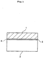
- Such proposals include, for instance, as shown in Fig. 3, a method for stabilizing the oxide/semiconductor interface, which comprises interposing a stable interface oxide (50) such as Y 2 O 3 , MgO, BiSiO 3 , etc., between a functional oxide (1) such as BaTiO 3 or SrTiO 3 , etc., and the semiconductor (2) such as a Si substrate.
- a stable interface oxide such as Y 2 O 3 , MgO, BiSiO 3 , etc.
- a functional oxide (1) such as BaTiO 3 or SrTiO 3 , etc.
- the semiconductor (2) such as a Si substrate.
- the stabilization is realized by the bonding that is formed between the elements constituting the interface oxide (50) and the dangling bonds of the elements constituting the semiconductor (2).
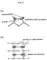
- Fig. 4 (A) shows schematically a part of the structure of a clean (001) surface of semiconductor Si that is highly reactive, because the outermost surface of the semiconductor Si consists of Si dimers having dangling bonds that are filled with two electrons and those having no electrons. Hence, an interface layer is formed between the semiconductor and the interface oxide as a result.
- an Object of the invention of the present application is to provide a method of stabilizing the oxide/semiconductor interface independent to temperature, which yet sufficiently realizes the performance of the functional oxide without forming an interface layer (reaction layer) between a semiconductor and the interface oxide, and to provide a stabilized semiconductor.
- the invention of the present application provides, in a first aspect, a method of stabilizing an oxide-semiconductor interface by using a Group 5 element, which comprises supplying an elemental Group 5 element or two or more types of Group 5 element to the surface of a semiconductor and growing an oxide on said Group 5 element, thereby stabilizing the interface between the oxide and the semiconductor.
- the invention of the present application provides, in a second aspect, a method of stabilizing an oxide-semiconductor interface by using a Group 5 element, wherein the semiconductor is silicon, the Group 5 element is As, and the oxide grown on the Group 5 element is a functional oxide such as CeO 2 , BaTiO 3 , PbZrTiO 3 , or SrTiO 3 .
- the invention of the present application provides, in a third aspect, a stabilized semiconductor the oxide-semiconductor interface thereof is stabilized by using a Group 5 element, in which the interface between the oxide and the semiconductor is stabilized by an oxide being grown on the surface of the semiconductor with an elemental Group 5 element or two or more types of Group 5 element being incorporated between them.
- the inventors of the present application extensively conducted studies, and, as a result, they have found that, by terminating the surface of the semiconductor with a Group 5 element, a surface structure having extremely low reactivity can be formed at the interface between the oxide and the semiconductor.
- the present invention has been accomplished based on these findings.
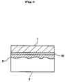
- a Group 5 element is supplied to the surface of a semiconductor (2) to cover the surface of the semiconductor with a coating layer (3) containing the Group 5 element, and a functional oxide (1) is grown thereon to stabilize an interface (4) between the oxide and the semiconductor.
- the method for supplying the Group 5 element to the surface of the semiconductor (2) is not particularly limited; for instance, a molecular beam of the Group 5 element may be supplied to the surface of the semiconductor after cleaning the surface by heating the semiconductor substrate in ultra-high vacuum, so that dimers of the Group 5 element may constitute the surface.
- any semiconductor (1) can be used without any particular limitation, and any type of semiconductors may be employed, e.g., the Group IV elements such as silicon, germanium, etc.; the Group III-VI compounds such as GaAs, InP, etc.; a hetero semiconductor; a piezo semiconductor; etc.
- the Group IV elements such as silicon, germanium, etc.
- the Group III-VI compounds such as GaAs, InP, etc.
- a hetero semiconductor such as GaAs, InP, etc.
- a piezo semiconductor etc.
- Group 5 element for use in the present invention, and there may be used Group 5A elements such as V, Nb, Ta, etc., as well as Group 5B elements such as N, P, As, Sb, Bi, etc.
- the Group 5 elements enumerated above may be used in the elemental form, but two or more types thereof may be supplied as well.
- a functional oxide (1) to be formed on the coating layer (3) using a Group 5 element in the present invention there maybe grown a dielectric material such as BaTiO 3 , SrTiO 3 , PbZrTiO 3 , etc., or a lattice matching oxide such as CeO 2 .
- a dielectric material such as BaTiO 3 , SrTiO 3 , PbZrTiO 3 , etc.
- a lattice matching oxide such as CeO 2 .
- the method according to the present invention greatly differs from a conventional one in that the oxide-semiconductor interface is stabilized by covering the surface of the semiconductor with a Group 5 element at a thickness of about 1 atomic layer.
- the performance of the functional oxide can be sufficiently exhibited yet without losing its function, because an interface layer (reaction layer) is not formed between the semiconductor and the interface oxide, but a stable oxide-semiconductor interface is established.
- a stable oxide-semiconductor interface can be formed independent to temperature.
- the invention according to the present invention is applicable in stably forming capacitors for use in memories of next generation integrated circuits, which, as a result, enables the implementation of a power-saving high-speed ferroelectric memory device capable of realizing high degree of integration, an application to an ultra-thin oxide film-semiconductor interface having a high dielectric Constant or a gate oxide film, an oxide-semiconductor superlattice, and a high efficiency light-emitting device.
- the stability of the oxide-semiconductor interface is described below by referring to its atomic structure.
- Fig. 2 (A) there is shown a surface structure in atomic scale of a (001) surface of a semiconductor, silicon (Si), covered with a Group 5 element, arsenic (As) . Dimers of As constitute the outermost surface of the semiconductor, and the dangling bonds of the dimers are filled with two electrons. Hence, the reactivity of the surface of As is lost. Thus, in the present invention as a result, which is greatly different from the conventional methods of stabilization, no interface layer (reaction layer) is formed between the semiconductor and the interface oxide.
- the atomic bonding of the As dimers (5) in the outermost layer with the Si atoms (6) in the lower layers is very strong, and this bonding is formed on the surface as a group of four atomic bonds. Hence, the resulting surface exhibits less reactivity. This results in a stabilized oxide-semiconductor interface.
- the surface stress can be relaxed by forming an As dimer having a long bonding length.
- the bonding between the As dimers and the Si atoms in the lower layer results with less strain, and the bonding is maintained to higher temperatures independent to the temperature. This greatly contributes to the stabilization of an oxide-semiconductor interface.
- a Si (001) substrate which is used as the semiconductor, was heated in ultrahigh vacuum to form a clean (001) surface. Then, by supplying a Group 5 element in the form of an As molecular beam on the surface of the semiconductor, a 2 ⁇ 1 structure of Si (001):As constructed from dimers of a Group 5 element, i.e., As, was formed on the semiconductor substrate. Then, CeO 2 was grown on the thus obtained sample as a functional oxide at a substrate temperature of 300 °C. For comparison, CeO 2 was grown on a cleaned surface of Si at the same temperature.
- the invention provides a method for stabilizing an oxide-semiconductor interface, which is free from the formation of an interface layer (reactive layer) between a semiconductor and an interface oxide and which thereby allows satisfactory exhibition of performance capabilities of a functional oxide and achievement of the stability of oxide-semiconductor interface, yet independent of temperature; it also provides a stabilized semiconductor, and a stabilized semiconductor implemented by the above method.
- the invention according to the present invention is applicable to the stable formation of capacitors for use in memories of next generation integrated circuits, which, as a result, enables the implementation of a power-saving high-speed ferroelectric memory device capable of high degree of integration, an application to an ultra-thin oxide film-semiconductor interface having a high dielectric constant or a gate oxide film, an oxide-semiconductor superlattice, and a high efficiency light-emitting device.
Landscapes
- Formation Of Insulating Films (AREA)
- Semiconductor Memories (AREA)
Applications Claiming Priority (3)
| Application Number | Priority Date | Filing Date | Title |
|---|---|---|---|
| JP32222799A JP2001144087A (ja) | 1999-11-12 | 1999-11-12 | 5族元素による酸化物/半導体界面の安定化方法と安定化半導体 |
| JP32222799 | 1999-11-12 | ||
| PCT/JP2000/007940 WO2001037330A1 (fr) | 1999-11-12 | 2000-11-10 | Procede de stabilisation d'une interface oxyde / semi-conducteur au moyen d'un element du groupe 5 et semi-conducteur stabilise |
Publications (3)
| Publication Number | Publication Date |
|---|---|
| EP1237183A1 true EP1237183A1 (fr) | 2002-09-04 |
| EP1237183A4 EP1237183A4 (fr) | 2006-02-15 |
| EP1237183B1 EP1237183B1 (fr) | 2011-01-19 |
Family
ID=18141363
Family Applications (1)
| Application Number | Title | Priority Date | Filing Date |
|---|---|---|---|
| EP00974913A Expired - Lifetime EP1237183B1 (fr) | 1999-11-12 | 2000-11-10 | Procede de stabilisation d'une interface oxyde / semi-conducteur au moyen d'un element du groupe 5 et semi-conducteur stabilise |
Country Status (7)
| Country | Link |
|---|---|
| US (1) | US6723164B1 (fr) |
| EP (1) | EP1237183B1 (fr) |
| JP (1) | JP2001144087A (fr) |
| KR (1) | KR100518395B1 (fr) |
| DE (1) | DE60045559D1 (fr) |
| TW (1) | TW490762B (fr) |
| WO (1) | WO2001037330A1 (fr) |
Cited By (1)
| Publication number | Priority date | Publication date | Assignee | Title |
|---|---|---|---|---|
| WO2012042442A1 (fr) * | 2010-09-28 | 2012-04-05 | International Business Machines Corporation | Dispositif à semi-conducteur doté d'un empilement de grilles |
Families Citing this family (17)
| Publication number | Priority date | Publication date | Assignee | Title |
|---|---|---|---|---|
| US6392257B1 (en) | 2000-02-10 | 2002-05-21 | Motorola Inc. | Semiconductor structure, semiconductor device, communicating device, integrated circuit, and process for fabricating the same |
| KR20030011083A (ko) | 2000-05-31 | 2003-02-06 | 모토로라 인코포레이티드 | 반도체 디바이스 및 이를 제조하기 위한 방법 |
| WO2002009157A2 (fr) * | 2000-07-21 | 2002-01-31 | Motorola, Inc. | Oxyde metallique alcalino-terreux sur des isolateurs de porte |
| AU2001277001A1 (en) | 2000-07-24 | 2002-02-05 | Motorola, Inc. | Heterojunction tunneling diodes and process for fabricating same |
| US20020096683A1 (en) | 2001-01-19 | 2002-07-25 | Motorola, Inc. | Structure and method for fabricating GaN devices utilizing the formation of a compliant substrate |
| WO2002082551A1 (fr) | 2001-04-02 | 2002-10-17 | Motorola, Inc. | Structure de semi-conducteur a courant de fuite attenue |
| US6992321B2 (en) | 2001-07-13 | 2006-01-31 | Motorola, Inc. | Structure and method for fabricating semiconductor structures and devices utilizing piezoelectric materials |
| US7019332B2 (en) | 2001-07-20 | 2006-03-28 | Freescale Semiconductor, Inc. | Fabrication of a wavelength locker within a semiconductor structure |
| US6855992B2 (en) | 2001-07-24 | 2005-02-15 | Motorola Inc. | Structure and method for fabricating configurable transistor devices utilizing the formation of a compliant substrate for materials used to form the same |
| US20030034491A1 (en) | 2001-08-14 | 2003-02-20 | Motorola, Inc. | Structure and method for fabricating semiconductor structures and devices for detecting an object |
| US20030071327A1 (en) | 2001-10-17 | 2003-04-17 | Motorola, Inc. | Method and apparatus utilizing monocrystalline insulator |
| US6916717B2 (en) | 2002-05-03 | 2005-07-12 | Motorola, Inc. | Method for growing a monocrystalline oxide layer and for fabricating a semiconductor device on a monocrystalline substrate |
| US7169619B2 (en) | 2002-11-19 | 2007-01-30 | Freescale Semiconductor, Inc. | Method for fabricating semiconductor structures on vicinal substrates using a low temperature, low pressure, alkaline earth metal-rich process |
| US6885065B2 (en) | 2002-11-20 | 2005-04-26 | Freescale Semiconductor, Inc. | Ferromagnetic semiconductor structure and method for forming the same |
| US7020374B2 (en) | 2003-02-03 | 2006-03-28 | Freescale Semiconductor, Inc. | Optical waveguide structure and method for fabricating the same |
| US6965128B2 (en) | 2003-02-03 | 2005-11-15 | Freescale Semiconductor, Inc. | Structure and method for fabricating semiconductor microresonator devices |
| WO2006051876A1 (fr) * | 2004-11-10 | 2006-05-18 | Dai Nippon Printing Co., Ltd. | Procede de fabrication d'un film d'oxyde metallique |
Family Cites Families (9)
| Publication number | Priority date | Publication date | Assignee | Title |
|---|---|---|---|---|
| JPH0614050A (ja) * | 1992-03-18 | 1994-01-21 | Fujitsu Ltd | Atm網における呼切断方法および該方法を行う交換機 |
| US5527567A (en) * | 1994-09-02 | 1996-06-18 | Ceram Incorporated | Metalorganic chemical vapor deposition of layered structure oxides |
| US5920775A (en) * | 1996-02-23 | 1999-07-06 | Vanguard International Semiconductor Corporation | Method for forming a storage capacitor within an integrated circuit |
| JPH10231196A (ja) * | 1996-12-17 | 1998-09-02 | Sony Corp | 酸化物積層構造の製造方法および有機金属化学気相成長装置 |
| JP3523093B2 (ja) * | 1997-11-28 | 2004-04-26 | 株式会社東芝 | 半導体装置およびその製造方法 |
| US6087208A (en) * | 1998-03-31 | 2000-07-11 | Advanced Micro Devices, Inc. | Method for increasing gate capacitance by using both high and low dielectric gate material |
| KR100297719B1 (ko) | 1998-10-16 | 2001-08-07 | 윤종용 | 박막제조방법 |
| JP2000183295A (ja) * | 1998-12-16 | 2000-06-30 | Matsushita Electronics Industry Corp | 半導体記憶装置及びその製造方法 |
| US20030015704A1 (en) * | 2001-07-23 | 2003-01-23 | Motorola, Inc. | Structure and process for fabricating semiconductor structures and devices utilizing the formation of a compliant substrate for materials used to form the same including intermediate surface cleaning |
-
1999
- 1999-11-12 JP JP32222799A patent/JP2001144087A/ja active Pending
-
2000
- 2000-11-10 US US10/129,983 patent/US6723164B1/en not_active Expired - Fee Related
- 2000-11-10 TW TW089123758A patent/TW490762B/zh not_active IP Right Cessation
- 2000-11-10 DE DE60045559T patent/DE60045559D1/de not_active Expired - Lifetime
- 2000-11-10 EP EP00974913A patent/EP1237183B1/fr not_active Expired - Lifetime
- 2000-11-10 WO PCT/JP2000/007940 patent/WO2001037330A1/fr not_active Ceased
- 2000-11-10 KR KR10-2002-7006120A patent/KR100518395B1/ko not_active Expired - Fee Related
Cited By (3)
| Publication number | Priority date | Publication date | Assignee | Title |
|---|---|---|---|---|
| WO2012042442A1 (fr) * | 2010-09-28 | 2012-04-05 | International Business Machines Corporation | Dispositif à semi-conducteur doté d'un empilement de grilles |
| GB2497257A (en) * | 2010-09-28 | 2013-06-05 | Ibm | Semiconductor device with a gate stack |
| GB2497257B (en) * | 2010-09-28 | 2013-11-06 | Ibm | Semiconductor device with a gate stack |
Also Published As
| Publication number | Publication date |
|---|---|
| EP1237183A4 (fr) | 2006-02-15 |
| TW490762B (en) | 2002-06-11 |
| WO2001037330A1 (fr) | 2001-05-25 |
| KR20020085891A (ko) | 2002-11-16 |
| EP1237183B1 (fr) | 2011-01-19 |
| US6723164B1 (en) | 2004-04-20 |
| JP2001144087A (ja) | 2001-05-25 |
| DE60045559D1 (de) | 2011-03-03 |
| KR100518395B1 (ko) | 2005-09-29 |
Similar Documents
| Publication | Publication Date | Title |
|---|---|---|
| US6723164B1 (en) | Method for stabilizing oxide-semiconductor interface by using group 5 element and stabilized semiconductor | |
| KR100676213B1 (ko) | 실리콘에 대해 안정적인 결정질의 경계면을 구비하는반도체 구조를 제작하기 위한 방법 | |
| US7351993B2 (en) | Rare earth-oxides, rare earth-nitrides, rare earth-phosphides and ternary alloys with silicon | |
| Nayfeh et al. | Effects of hydrogen annealing on heteroepitaxial-Ge layers on Si: Surface roughness and electrical quality | |
| CN1185689C (zh) | 具有结晶碱土金属硅氮化物/氧化物与硅界面的半导体结构 | |
| US20100140755A1 (en) | Rare-earth oxides, rare-earth nitrides, rare-earth phosphides and ternary alloys | |
| US20050163692A1 (en) | Rare earth-oxides, rare earth -nitrides, rare earth -phosphides and ternary alloys with silicon | |
| Wang et al. | Interface and tunneling barrier heights of NbN/AlN/NbN tunnel junctions | |
| US20090001329A1 (en) | Rare earth-oxides, rare earth-nitrides, rare earth-phosphies, and ternary alloys with silicon | |
| EP1043426A1 (fr) | Méthode de formation d'une structure semiconductrice comprenant une monocouche atomique constituée de métal alcalino-terreux, d'oxygène et de silicium en tant que couche d'interface entre un substrat de silicium et une couche d'oxyde monocristallin | |
| US20050156155A1 (en) | Rare earth-oxides, rare earth-nitrides, rare earth-phosphides and ternary alloys with silicon | |
| WO2002058164A2 (fr) | Dispositif a base de gan presentant un substrat souple | |
| WO2005065402A2 (fr) | Oxydes, nitrures et phosphures de terres rares, et alliages ternaires au silicium | |
| JPH10289906A (ja) | Iii−v族エピタキシャル・ウェハ製造 | |
| KR100516252B1 (ko) | 반도체소자를가진물품및그제조방법 | |
| Martrou et al. | Equilibrium shape of steps and islands on polar II-VI semiconductors surfaces | |
| US5571391A (en) | Electrode structure and method for fabricating the same | |
| Oral et al. | Initial stages of SiGe epitaxy on Si (001) studied by scanning tunneling microscopy | |
| KR20030051820A (ko) | 고 유전 상수 재료를 가지는 반도체 구조체 | |
| Haraguchi et al. | The growth mechanism of nanometer-scale GaAs, InAs, and AlGaAs whiskers | |
| JP7744830B2 (ja) | 半導体構造および方法 | |
| Kim et al. | Microstructural and electrical properties of MgO thin films grown on p-GaAs (100) substrates | |
| Ide et al. | STM observation of growth interruption effect of MBE growth | |
| US20050211970A1 (en) | Metal nano-objects, formed on semiconductor surfaces, and method for making said nano-objects | |
| Kubo et al. | Direct Observation of Strained Layer Formation at the Initial Stage of In Thin Film Growth on Si (100) |
Legal Events
| Date | Code | Title | Description |
|---|---|---|---|
| PUAI | Public reference made under article 153(3) epc to a published international application that has entered the european phase |
Free format text: ORIGINAL CODE: 0009012 |
|
| 17P | Request for examination filed |
Effective date: 20020612 |
|
| AK | Designated contracting states |
Kind code of ref document: A1 Designated state(s): AT BE CH CY DE DK ES FI FR GB GR IE IT LI LU MC NL PT SE TR |
|
| RBV | Designated contracting states (corrected) |
Designated state(s): AT BE CH CY DE FR GB LI NL |
|
| RAP1 | Party data changed (applicant data changed or rights of an application transferred) |
Owner name: JAPAN AS REPRESENTED BY DIRECTOR GENERAL OF NATION Owner name: JAPAN SCIENCE AND TECHNOLOGY AGENCY |
|
| A4 | Supplementary search report drawn up and despatched |
Effective date: 20060103 |
|
| RAP1 | Party data changed (applicant data changed or rights of an application transferred) |
Owner name: NATIONAL INSTITUTE FOR MATERIALS SCIENCE |
|
| GRAP | Despatch of communication of intention to grant a patent |
Free format text: ORIGINAL CODE: EPIDOSNIGR1 |
|
| GRAS | Grant fee paid |
Free format text: ORIGINAL CODE: EPIDOSNIGR3 |
|
| GRAA | (expected) grant |
Free format text: ORIGINAL CODE: 0009210 |
|
| AK | Designated contracting states |
Kind code of ref document: B1 Designated state(s): DE FR GB NL |
|
| REG | Reference to a national code |
Ref country code: GB Ref legal event code: FG4D |
|
| REF | Corresponds to: |
Ref document number: 60045559 Country of ref document: DE Date of ref document: 20110303 Kind code of ref document: P |
|
| REG | Reference to a national code |
Ref country code: DE Ref legal event code: R096 Ref document number: 60045559 Country of ref document: DE Effective date: 20110303 |
|
| REG | Reference to a national code |
Ref country code: NL Ref legal event code: T3 |
|
| PLBE | No opposition filed within time limit |
Free format text: ORIGINAL CODE: 0009261 |
|
| STAA | Information on the status of an ep patent application or granted ep patent |
Free format text: STATUS: NO OPPOSITION FILED WITHIN TIME LIMIT |
|
| 26N | No opposition filed |
Effective date: 20111020 |
|
| REG | Reference to a national code |
Ref country code: DE Ref legal event code: R097 Ref document number: 60045559 Country of ref document: DE Effective date: 20111020 |
|
| PGFP | Annual fee paid to national office [announced via postgrant information from national office to epo] |
Ref country code: FR Payment date: 20121130 Year of fee payment: 13 Ref country code: DE Payment date: 20121121 Year of fee payment: 13 |
|
| PGFP | Annual fee paid to national office [announced via postgrant information from national office to epo] |
Ref country code: GB Payment date: 20121120 Year of fee payment: 13 |
|
| PGFP | Annual fee paid to national office [announced via postgrant information from national office to epo] |
Ref country code: NL Payment date: 20121120 Year of fee payment: 13 |
|
| REG | Reference to a national code |
Ref country code: NL Ref legal event code: V1 Effective date: 20140601 |
|
| GBPC | Gb: european patent ceased through non-payment of renewal fee |
Effective date: 20131110 |
|
| REG | Reference to a national code |
Ref country code: FR Ref legal event code: ST Effective date: 20140731 |
|
| PG25 | Lapsed in a contracting state [announced via postgrant information from national office to epo] |
Ref country code: NL Free format text: LAPSE BECAUSE OF NON-PAYMENT OF DUE FEES Effective date: 20140601 Ref country code: DE Free format text: LAPSE BECAUSE OF NON-PAYMENT OF DUE FEES Effective date: 20140603 |
|
| REG | Reference to a national code |
Ref country code: DE Ref legal event code: R119 Ref document number: 60045559 Country of ref document: DE Effective date: 20140603 |
|
| PG25 | Lapsed in a contracting state [announced via postgrant information from national office to epo] |
Ref country code: GB Free format text: LAPSE BECAUSE OF NON-PAYMENT OF DUE FEES Effective date: 20131110 Ref country code: FR Free format text: LAPSE BECAUSE OF NON-PAYMENT OF DUE FEES Effective date: 20131202 |