EP1237141A2 - Light-producing high aperture display having aligned tiles - Google Patents
Light-producing high aperture display having aligned tiles Download PDFInfo
- Publication number
- EP1237141A2 EP1237141A2 EP02075559A EP02075559A EP1237141A2 EP 1237141 A2 EP1237141 A2 EP 1237141A2 EP 02075559 A EP02075559 A EP 02075559A EP 02075559 A EP02075559 A EP 02075559A EP 1237141 A2 EP1237141 A2 EP 1237141A2
- Authority
- EP
- European Patent Office
- Prior art keywords
- tile
- pixels
- aperture ratio
- tiles
- high aperture
- Prior art date
- Legal status (The legal status is an assumption and is not a legal conclusion. Google has not performed a legal analysis and makes no representation as to the accuracy of the status listed.)
- Withdrawn
Links
Images


Classifications
-
- G—PHYSICS
- G02—OPTICS
- G02F—OPTICAL DEVICES OR ARRANGEMENTS FOR THE CONTROL OF LIGHT BY MODIFICATION OF THE OPTICAL PROPERTIES OF THE MEDIA OF THE ELEMENTS INVOLVED THEREIN; NON-LINEAR OPTICS; FREQUENCY-CHANGING OF LIGHT; OPTICAL LOGIC ELEMENTS; OPTICAL ANALOGUE/DIGITAL CONVERTERS
- G02F1/00—Devices or arrangements for the control of the intensity, colour, phase, polarisation or direction of light arriving from an independent light source, e.g. switching, gating or modulating; Non-linear optics
- G02F1/01—Devices or arrangements for the control of the intensity, colour, phase, polarisation or direction of light arriving from an independent light source, e.g. switching, gating or modulating; Non-linear optics for the control of the intensity, phase, polarisation or colour
- G02F1/13—Devices or arrangements for the control of the intensity, colour, phase, polarisation or direction of light arriving from an independent light source, e.g. switching, gating or modulating; Non-linear optics for the control of the intensity, phase, polarisation or colour based on liquid crystals, e.g. single liquid crystal display cells
- G02F1/133—Constructional arrangements; Operation of liquid crystal cells; Circuit arrangements
-
- G—PHYSICS
- G09—EDUCATION; CRYPTOGRAPHY; DISPLAY; ADVERTISING; SEALS
- G09G—ARRANGEMENTS OR CIRCUITS FOR CONTROL OF INDICATING DEVICES USING STATIC MEANS TO PRESENT VARIABLE INFORMATION
- G09G3/00—Control arrangements or circuits, of interest only in connection with visual indicators other than cathode-ray tubes
- G09G3/20—Control arrangements or circuits, of interest only in connection with visual indicators other than cathode-ray tubes for presentation of an assembly of a number of characters, e.g. a page, by composing the assembly by combination of individual elements arranged in a matrix no fixed position being assigned to or needed to be assigned to the individual characters or partial characters
-
- H—ELECTRICITY
- H10—SEMICONDUCTOR DEVICES; ELECTRIC SOLID-STATE DEVICES NOT OTHERWISE PROVIDED FOR
- H10K—ORGANIC ELECTRIC SOLID-STATE DEVICES
- H10K59/00—Integrated devices, or assemblies of multiple devices, comprising at least one organic light-emitting element covered by group H10K50/00
- H10K59/10—OLED displays
- H10K59/18—Tiled displays
-
- G—PHYSICS
- G06—COMPUTING OR CALCULATING; COUNTING
- G06F—ELECTRIC DIGITAL DATA PROCESSING
- G06F3/00—Input arrangements for transferring data to be processed into a form capable of being handled by the computer; Output arrangements for transferring data from processing unit to output unit, e.g. interface arrangements
- G06F3/14—Digital output to display device ; Cooperation and interconnection of the display device with other functional units
- G06F3/1423—Digital output to display device ; Cooperation and interconnection of the display device with other functional units controlling a plurality of local displays, e.g. CRT and flat panel display
- G06F3/1446—Digital output to display device ; Cooperation and interconnection of the display device with other functional units controlling a plurality of local displays, e.g. CRT and flat panel display display composed of modules, e.g. video walls
-
- G—PHYSICS
- G09—EDUCATION; CRYPTOGRAPHY; DISPLAY; ADVERTISING; SEALS
- G09G—ARRANGEMENTS OR CIRCUITS FOR CONTROL OF INDICATING DEVICES USING STATIC MEANS TO PRESENT VARIABLE INFORMATION
- G09G2300/00—Aspects of the constitution of display devices
- G09G2300/02—Composition of display devices
- G09G2300/026—Video wall, i.e. juxtaposition of a plurality of screens to create a display screen of bigger dimensions
-
- H—ELECTRICITY
- H10—SEMICONDUCTOR DEVICES; ELECTRIC SOLID-STATE DEVICES NOT OTHERWISE PROVIDED FOR
- H10K—ORGANIC ELECTRIC SOLID-STATE DEVICES
- H10K59/00—Integrated devices, or assemblies of multiple devices, comprising at least one organic light-emitting element covered by group H10K50/00
- H10K59/10—OLED displays
- H10K59/12—Active-matrix OLED [AMOLED] displays
- H10K59/131—Interconnections, e.g. wiring lines or terminals
Definitions
- the present invention relates to high aperture ratio displays, which include a plurality of tiles aligned to produce an image.
- Flat panel displays are found everywhere from hand held electronics to large scale video applications. Larger displays are usually smaller displays tiled together. When the displays are tiled it is important to create a bright image that appears seamless across the tiles.
- the image brightness is proportional to the size of the aperture ratio in the display as defined by the ratio of the emissive surface area of a pixel to the total surface area of the same pixel. Increasing the aperture ratio of the pixel produces a brighter image. However, increasing the space between pixels allows for a proportional increase in the spacing between adjacent tiles, thereby facilitating the ability to create a seamless tiled display. Therefore, any increase in the area available for each pixel can be distributed optimally to increase the aperture ratio, and to increase the space available between pixels including the space between adjacent pixels on abutting tiles.
- LCD liquid crystal displays
- LCD's liquid crystal displays
- the liquid crystal material when activated by an electric field, acts as a valve to transmit light from a back light source.
- LCD's require a transparent path that includes a transparent substrate and transparent pixel electrodes. There cannot be anything blocking the pixel from the backlight.
- video LCD displays the space available for creating seams between tiles is limited by the rows of circuits that fill the space between pixels.
- US-A-5,056,893 describes a technique in which there is increased space for a seam by making the pixels at the edge of a tile smaller. Reducing the size of the pixels is a significant trade-off in brightness and image quality.
- US-A-5,903,328 describes tiled LCD displays where the adjacent tile edges are ground at an angle and overlap each other. This allows a small increase in the space for the ground edge relative to the adjacent pixels; however, as the space increases the distance between the image planes of adjacent tiles increases proportionally.
- US-A-6,136,621 describes a method for making a high aspect ratio gated emitter wherein the lower gate is partially covered by an insulator and the upper gate; the lower gate extends through a hole in the insulator and the upper gate.
- US-A-5,955,744 describes a LCD display wherein the TFT is under the pixel electrode, located just outside the perimeter of the pixel so as not to block light from the backlight.
- Emissive displays which produce their own light, do not require a transparent substrate.
- the pixels do not have to be positioned over a transparent substrate or a transparent electrode. This allows for stacking of the integrated drive circuits and the circuits under the light-emitting layer which contains only an array of light-emitting pixels.
- These tiles can be arrayed together to make a monolithic tiled display wherein the pixel pitch across the seam of adjacent tiles is substantially equal to that of the pixel pitch within a tile.
- the pixels on each tile are addressed through vertical connections and a conductor layer to the corresponding circuits.
- the drive circuits are semiconductor electronics that are manufactured directly on the substrate and can be on the same level as the circuits or under the circuits.
- the drive circuits can also be located on the bottom side of the substrate and connected using vertically connections through the substrate.
- US-A-6,091,194 describes an emissive display tile in which discrete drive circuits are attached to the bottom side of the tile.
- a high aperture ratio display comprising:
- the pixel aperture ratio can be larger than that of prior art in a tiled display.
- This high aperture ratio on the light-emitting surface can be achieved by eliminating the need to share space with the electronics.
- the pixels can extend to all edges of each display tile wherein the circuits and conductors are on layers under the pixels and are contained in an area defined by the outermost pixels on each tile.
- the increased space allowed for each pixel can provide additional space between pixels.
- the total area available for each pixel can be optimized to establish a large pixel in conjunction with adequate space between pixels.
- the space between pixels determines the space available for the seam between two or more tiles that are positioned adjacently to create a tiled display.
- a high aperture ratio tiled display can be an array of tiles that include island tiles, tiles that do not have an edge along the perimeter of the display. This is accomplished by extending the pixels to all edges of a tile and by utilizing vertical connections to address each pixel.
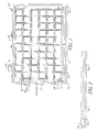
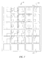
- FIGS. 1 and 2 show a prior art for a tiled display 40 having a plurality of tiles 16a-16b each with circuits 26 and drive circuits 22 and pixel electrodes 104 or 304.
- the drive circuits 22, circuits 26 and pixel electrodes 104 or 304 for each tile 16a-16b exist in the same circuit layer.
- the circuit 26 includes the thin film transistors and associated capacitors.
- the pixel aperture ratio is limited by the space required for the circuits 26 and, furthermore, the drive circuits 22 extend beyond the area defined by the outermost pixels on each tile.
- the drive circuits 22 are separate discrete components that are interconnected to the tile using tape automated bonding or other means.
- the horizontal pitch 80 between adjacent pixels on adjacent tiles, across a seam is substantially equivalent to the horizontal pixel pitch 80 on a single tile. Additionally, the vertical pixel pitch 82 and the horizontal pixel pitch 80 are substantially the same for all tiles in the display.
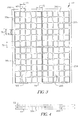
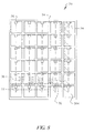
- an emissive tiled display 42 is comprised of two or more emissive tiles 20a-d arrayed, or tiled, together to provide a monolithic seamless display.
- the stacking of the circuits 26 and drive circuits 22 under the pixels on each tile allows for pixels 300 to be positioned near the edge of tiles 20a-20d with the distance from the outermost pixel edge to the tile edge at most equal to one-half the space between pixels 300.
- the integration of the drive circuits 22 onto each tile reduces the number of external signal connections 34 needed.
- the stacking of the drive circuits 22 under the pixels allows for the external signal connections 34 to be made in the limited space at the edge of the tile 20, or alternately, through vertical connections 36 to the back of the tile 20.
- a conductor can be provided along a tile edge to an adjacent tile for the purpose of carrying electrical signals out to the edge of a perimeter tile.
- the vertical 76 and horizontal pitch 72 between adjacent pixels on adjacent tiles, across a seam, is substantially equivalent to the vertical 76 and horizontal 72 pixel pitch on a single tile. Additionally, the vertical 76 and horizontal 72 pixel pitch is substantially the same for all tiles in the display.
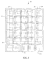
- FIG. 5 shows a composite view of an emissive multilayer tile 20 from the tiled display shown in FIG. 3.
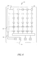
- FIG.6 shows the drive circuits 22 and the circuits 26 that are located on the same plane on the tile 20 and are electrically connected by connectors 24.
- the tile 20 does not have to be transparent but may be any material compatible with TFT processing including, but not limited to, glass and co-fired ceramic.
- the pixel electrodes 304 are located above the circuits 26 and separated by insulating layers 60 and 66 shown in cross-sections FIGS. 11-13.
- FIG. 7 shows the circuits 26 connected to the pixel electrodes 304 by means of an additional layer containing a plurality of conductors 28 shown between the insulating layers 60 and 66 in FIGS. 11-14. Also shown in these figures are the components of the TFT circuits: source 30, insulating layer 58, gate insulator 64, anisotropic silicon 68, and drain 70. It is the preferred embodiment that the drive circuits 22 and circuits 26 are contained in an area defined by the outermost pixels wherein drive circuits 22 and circuits 26 do not extend past the outermost pixels. It is understood that each circuit 26 is not necessarily located directly under the corresponding pixel electrode 304. The circuits 26 are electrically connected to the pixel electrode 304 through vertical connections and interconnections 28.
- the connections to the drive circuits can be made through vertical connections 36 that extend to the backside of the tile 20.
- the external interconnections to the drive circuits 22 can extend to one or more edges of the tile 20, beyond the outermost pixel.
- the drive circuits 22 are integrated on a separate layer under the circuits.
- circuits 26 reside above the drive circuits 22 and are separated from the drive circuits by an insulating layer.
- the pixel electrodes 304 are located above the circuits 26, separated by another insulating layer.
- the interconnections 24 from the drive circuits 22 to the circuits 26 and from the circuits 26 to the pixel electrodes 304 are made using vertical connections 36.
- a layer containing a plurality of conductors 28 can be used to connect the circuits 26 to the pixel electrodes 304.
- External signal connections 34 to the drive circuits can be made along one or more edges of the tile 20, or through vertical connections 36 to the backside of the tile 20 and on to the drive circuits through drive circuit signal connections 32.
- the drive circuits 22 are integrated on the backside of the tile 20.
- the drive circuits 22 are electrically connected to the topside circuits 26 through the tile 20 using vertical connections 36. It is understood that double side TFT processing is required on the tile.
- a layer containing a plurality of conductors 28 can be used to connect circuits 26 that are offset from the pixels electrodes 304 to the pixel electrodes 304.
- External signal connections 34 to the drive circuits 22 can be made to the backside of the tile 20.
- FIG. 11 shows the cross-section of the multilayer emissive tile 20.
- the drive circuits 22 and circuits 26 are electrically connected to the pixels 300 through the conductor layer 28.
- the display includes a cover plate 52 and the display is viewed through the cover plate 52.
- the cover plate 52 is a transparent substrate and includes, but is not limited to, glass and plastic. It is understood that a material 56 that has matching index of refraction to the cover plate 52 can be used to fill any gaps between the pixels 300 and the cover plate 52. This material can also provide moisture and oxygen protection.
- the cover plate 52 includes a polarization layer 50 to increase the contrast ratio of the display.
- the cover plate 52 includes a color filter array 54.
- the patterned color filter array 54 is aligned with the pixel array.
- a color filter array 54 is employed on the cover plate 52 the pixels 300 are understood to be white light-emitting.
- the light-emitting layer 308 can be a continuous coating as shown.
- the cover plate 52 is bonded to the emissive tile 20 by means including, but not limited to, adhesive, metal and solgel.
- a desiccant can be positioned in or near the seals between the tile 20 and the cover plate 52.
- an oxygen getter can be positioned in or near the seals between the tile 20 and the cover plate 52.
- the tiles are positioned between the cover plate 52 and a back plate 18.
- the tiles can be affixed to either the cover plate 52 or back plate 18.
- the back plate 18 does not need to be transparent.
- electrical connections can be made from the tile to the back plate 18.
- the cover plate 52 and back plate 18 are sealed around the perimeter enclosing the tile array within.
- a desiccant may also be positioned in or near any of the seals previously described. Alternately, an oxygen getter is positioned in or near any of the seals previously described.
- the present invention is applicable to emissive displays, and is particularly suitable for, but not limited to, use in organic electroluminescent displays.
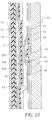
- FIGS. 14 and 15 describe examples of pixels with organic electroluminescent materials.
- a light-emitting layer of an organic electroluminescent tile comprises a luminescent or fluorescent material where electroluminescence is produced as a result of electron-hole pair recombination in this region.
- the light-emitting layer 108 is sandwiched between pixel electrode 104 that is an anode and the cathode 106.
- the light-emitting layer 108 is a pure material with a high luminescent efficiency.
- a well known material is tris (8-quinolinato) aluminum, (Alq), which produces excellent green electroluminescence.
- the simple pixel structure 100 can be modified to a multilayer structure in which an additional electroluminescent layer is introduced between the hole and electron-transporting layers to function primarily as the site for hole-electron recombination and thus electroluminescence.
- the functions of the individual organic layers are distinct and can therefore be optimized independently.
- the electroluminescent or recombination layer can be chosen to have a desirable EL color as well as high luminance efficiency.
- the electron and hole transport layers can be optimized primarily for the carrier transport property.
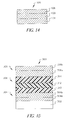
- the pixel 100 is described as a multilayer organic device that emits light from the top.
- the multilayer organic device 300 has a substrate 302 on which is disposed a light reflective conductive anode 304.
- the anode 304 comprises two layers including a light reflective conductive metal layer 304a and a thin transparent layer of a conductive high work function material 304b.
- An organic light-emitting structure 308 is formed between the anode 304 and a cathode 306.
- the cathode 306 is composed of two layers including a thin transparent conductive layer of a low work function material 306a and a transparent conductive layer such as indium tin oxide 306b.
- the organic light-emitting structure 308 is comprised of, in sequence, an organic hole-transporting layer 310, an organic light-emitting layer 312, and an organic electron-transporting layer 314.
- an electrical potential difference (not shown) is applied between the anode 304 and the cathode 306, the cathode will inject electrons into the electron-transporting layer 314, and the electrons will migrate across layer 314 to the light-emitting layer 312.
- holes will be injected from the anode 304 into the hole-transporting layer 310.
- the holes will migrate across layer 310 and recombine with electrons at or near a junction formed between the hole-transporting layer 310 and the light-emitting layer 312.
- a migrating electron drops from its conduction band to a valence band in filling a hole, energy is released as light, and is emitted through the light-transmissive cathode 306.
- the high aperture ratio display wherein at least one tile edge is parallel to the pixel row or column and the distance from said edge of the tile to the outermost row or column of pixels is about one half of the space between pixels.
- the high aperture ratio display wherein the tiles are mounted to a transparent cover plate by bonding means including, but not limited to, adhesive or metal, and the high aperture ratio display is viewed through the cover plate.
- the high aperture ratio display wherein the tiles are mounted to a transparent cover plate by bonding means including, but not limited to, adhesive or metal, and the high aperture ratio display is viewed through the cover plate.
- the high aperture ratio display wherein a polarization layer is over the viewing side of the cover plate.
- the high aperture ratio display wherein a polarization layer is over the viewing side of the cover plate.
- the high aperture ratio display wherein the pixels emit monochromatic light and wherein filters of different colors are disposed on the cover plate and are aligned to the pixels thereby providing full color capability, and furthermore, the filters are located on the side of the cover plate next to the pixels.
- the high aperture ratio display wherein the pixels emit monochromatic light and wherein filters of different colors are disposed on the cover plate and are aligned to the pixels thereby providing full color capability, and furthermore, the filters are located on the side next to the white light-emitting pixels.
- the high aperture ratio display wherein the pixels emit different color light and the pixels being arranged in a pattern to produce a full-color high aperture ratio display.
- the high aperture ratio display wherein the pixels emit different color light and the pixels being arranged in a pattern to produce a full-color high aperture ratio display.
- the high aperture ratio display wherein the high aperture ratio display is further mounted to a back plate.
- the high aperture ratio display wherein the high aperture ratio display is further mounted to a back plate.
- the high aperture ratio display wherein at least one conductor is provided along a tile edge to an adjacent tile and furthermore the conductor terminates on an outer edge of the high aperture ratio display.
- the high aperture ratio display wherein at least one conductor is provided along a tile edge to an adjacent tile and furthermore the conductor terminates on an outer edge of the high aperture ratio display.
- the high aperture ratio display wherein the pixel aperture ratio is at least 60%.
- the high aperture ratio display wherein the pixel aperture ratio is at least 60%.
Landscapes
- Physics & Mathematics (AREA)
- Engineering & Computer Science (AREA)
- General Physics & Mathematics (AREA)
- Computer Hardware Design (AREA)
- Theoretical Computer Science (AREA)
- Nonlinear Science (AREA)
- Mathematical Physics (AREA)
- Chemical & Material Sciences (AREA)
- Crystallography & Structural Chemistry (AREA)
- Optics & Photonics (AREA)
- Electroluminescent Light Sources (AREA)
- Devices For Indicating Variable Information By Combining Individual Elements (AREA)
Abstract
Description
Claims (10)
- A high aperture ratio display comprising:a) at least two tiles having rows and columns of electric fieldactuable pixels which produce light from one surface of each tile, the pitch between each column of each tile being substantially the same and the pitch between each row of each tile being substantially the same, the tiles being arranged so that, when aligned, the pitch between adjacent pixels on adjacent tiles is the same so that when light is emitted from the surface of the tiles, it does not have intertile artifacts;b) a plurality of conductors disposed under the pixels of each tile and arranged to provide an electrical connection between the pixels of each tile; andc) circuits electrically connected to the conductors for producing electrical signals which cause the emission of light in the pixels of each tile to produce an image.
- The high aperture ratio display of claim 1 wherein the conductors are fabricated on the tiles and wherein the electrically connected circuits further include at least one layer on each tile having thin film transistors connected to the conductors.
- The high aperture ratio display of claim 2 wherein the electrically connected circuits include drive circuits connected to the thin film transistors for multiplex operation of the transistors to cause electrical signals to be provided to the pixels to produce a video image.
- A high aperture ratio display comprising:a) a back plate;b) at least two tiles having rows and columns of electric field actuable pixels which produce light from one surface of each tile, the pitch between each column of each tile being substantially the same and the pitch between each row of each tile being substantially the same, the tiles being arranged so that, when aligned and mounted on the back plate, the pitch between adjacent pixels in adjacent tiles is the same so that when light is emitted from the surface of the tiles, it does not have intertile artifacts;c) a plurality of conductors connected to the pixels of each tile and a layer disposed on the non-emissive surface of each tile and formed with a plurality of thin film transistors connected to the conductors; andd) drive circuits fabricated on each tile or on the back plate and electrically connected to the thin film transistors for producing electrical signals for multiplex operation of the transistors to cause the electrical signals to be provided to the pixels to produce a video image.
- The high aperture ratio display of claim 4 wherein each tile further includes a first layer having the thin film transistors and a second layer located under the first layer and containing the drive circuits and wherein both the first and second layer are contained in an area defined by the outermost pixels of the tile.
- The high aperture ratio display of claim 4 wherein the drive circuits, the electrically connected circuits, and the conductors on each tile are each contained in an area defined by the outermost pixels of the tile.
- The high aperture ratio display of claim 2 wherein at least one conductor connection to the electrical circuits extends past the outermost pixels and terminates along one or more of the edges of the tile.
- The high aperture ratio display of claim 3 wherein at least one conductor line to the drive circuits extends past the pixel array and terminates along one or more of the edges of the tile.
- The high aperture ratio display of claim 4 wherein at least one signal line to the drive circuits extends past the outermost pixels and terminates along one or more of the edges of the tile.
- The high aperture ratio display of claim 1 wherein at least one tile edge is parallel to the pixel row or column and the distance from said edge of the tile to the outermost row or column of pixels is about one half of the space between pixels.
Applications Claiming Priority (2)
| Application Number | Priority Date | Filing Date | Title |
|---|---|---|---|
| US09/788,923 US6853411B2 (en) | 2001-02-20 | 2001-02-20 | Light-producing high aperture ratio display having aligned tiles |
| US788923 | 2004-02-27 |
Publications (2)
| Publication Number | Publication Date |
|---|---|
| EP1237141A2 true EP1237141A2 (en) | 2002-09-04 |
| EP1237141A3 EP1237141A3 (en) | 2006-04-12 |
Family
ID=25146007
Family Applications (1)
| Application Number | Title | Priority Date | Filing Date |
|---|---|---|---|
| EP02075559A Withdrawn EP1237141A3 (en) | 2001-02-20 | 2002-02-08 | Light-producing high aperture display having aligned tiles |
Country Status (5)
| Country | Link |
|---|---|
| US (1) | US6853411B2 (en) |
| EP (1) | EP1237141A3 (en) |
| JP (1) | JP2002268589A (en) |
| KR (1) | KR20020068284A (en) |
| TW (1) | TWI243626B (en) |
Cited By (7)
| Publication number | Priority date | Publication date | Assignee | Title |
|---|---|---|---|---|
| WO2003052825A1 (en) * | 2001-12-17 | 2003-06-26 | Koninklijke Philips Electronics N.V. | Tiled flat panel display, method of manufacturing the same, and sub-display for use in such a display, and method of driving such a display |
| US6674492B1 (en) * | 1999-04-13 | 2004-01-06 | Mitsubishi Rayon Co., Ltd. | Filter and image device with filter |
| WO2006057802A3 (en) * | 2004-11-23 | 2006-11-09 | Eastman Kodak Co | Tiled display |
| WO2013068912A1 (en) * | 2011-11-08 | 2013-05-16 | Koninklijke Philips Electronics N.V. | Seamless tiling to build a large detector |
| WO2014036736A1 (en) * | 2012-09-10 | 2014-03-13 | 深圳市柔宇科技有限公司 | Large-size display screen and manufacturing method therefor |
| US11164934B2 (en) * | 2019-03-12 | 2021-11-02 | X Display Company Technology Limited | Tiled displays with black-matrix support screens |
| WO2024200379A1 (en) * | 2023-03-24 | 2024-10-03 | Barco N.V. | Display device and method to manufacture the display device |
Families Citing this family (42)
| Publication number | Priority date | Publication date | Assignee | Title |
|---|---|---|---|---|
| JP2004140267A (en) * | 2002-10-18 | 2004-05-13 | Semiconductor Energy Lab Co Ltd | Semiconductor device and manufacturing method thereof |
| WO2005004544A1 (en) * | 2003-07-07 | 2005-01-13 | Ifire Technology Corp. | Seal and sealing process for electroluminescent displays |
| JP4623701B2 (en) * | 2003-08-29 | 2011-02-02 | 株式会社 日立ディスプレイズ | Coloring composition for color filter and display device using color filter formed with this coloring composition |
| EP2078229A2 (en) * | 2006-11-02 | 2009-07-15 | Sensics, Inc. | Systems and methods for a head-mounted display |
| US7995002B2 (en) * | 2007-09-19 | 2011-08-09 | Global Oled Technology Llc | Tiled passive matrix electro-luminescent display |
| KR101415571B1 (en) * | 2007-10-15 | 2014-07-07 | 삼성디스플레이 주식회사 | Display device and driving method of the same |
| US8085216B2 (en) * | 2007-10-17 | 2011-12-27 | The United States Of America As Represented By The Secretary Of The Navy | Real time desktop image warping system |
| US9013367B2 (en) * | 2008-01-04 | 2015-04-21 | Nanolumens Acquisition Inc. | Flexible display |
| EP2110801A3 (en) | 2008-04-15 | 2010-01-06 | Element Labs, Inc. | Isolating alignment and structural strength in LED display systems |
| EP2304710B1 (en) | 2008-06-13 | 2014-08-13 | Barco, Inc. | Alignment angle method and apparatus for a display |
| US9400212B2 (en) | 2008-06-13 | 2016-07-26 | Barco Inc. | Smart pixel addressing |
| US9899329B2 (en) | 2010-11-23 | 2018-02-20 | X-Celeprint Limited | Interconnection structures and methods for transfer-printed integrated circuit elements with improved interconnection alignment tolerance |
| US8934259B2 (en) | 2011-06-08 | 2015-01-13 | Semprius, Inc. | Substrates with transferable chiplets |
| WO2013059489A1 (en) * | 2011-10-18 | 2013-04-25 | Reald Inc. | Electronic display tiling apparatus and propagation based method thereof |
| US9361059B2 (en) | 2012-12-14 | 2016-06-07 | Intel Corporation | Architecture for seamless integrated display system |
| US9799719B2 (en) | 2014-09-25 | 2017-10-24 | X-Celeprint Limited | Active-matrix touchscreen |
| US9557954B2 (en) | 2014-12-23 | 2017-01-31 | X Development Llc | Display panel using direct emission pixel arrays |
| CN104750451B (en) * | 2015-04-10 | 2017-10-31 | 京东方科技集团股份有限公司 | Splicer and splice displaying system |
| TWI710061B (en) | 2016-02-25 | 2020-11-11 | 愛爾蘭商艾克斯展示公司技術有限公司 | Efficiently micro-transfer printing micro-scale devices onto large-format substrates |
| US10395966B2 (en) | 2016-11-15 | 2019-08-27 | X-Celeprint Limited | Micro-transfer-printable flip-chip structures and methods |
| US10600671B2 (en) | 2016-11-15 | 2020-03-24 | X-Celeprint Limited | Micro-transfer-printable flip-chip structures and methods |
| EP3542394B1 (en) | 2016-11-15 | 2025-09-24 | X Display Company Technology Limited | Micro-transfer-printable flip-chip structures and manufacturing methods thereof |
| US11024608B2 (en) | 2017-03-28 | 2021-06-01 | X Display Company Technology Limited | Structures and methods for electrical connection of micro-devices and substrates |
| US10468397B2 (en) | 2017-05-05 | 2019-11-05 | X-Celeprint Limited | Matrix addressed tiles and arrays |
| TWI781241B (en) | 2017-11-08 | 2022-10-21 | 美商康寧公司 | Apparatus and methods for assembling a display area |
| US11527519B2 (en) | 2017-11-27 | 2022-12-13 | Seoul Viosys Co., Ltd. | LED unit for display and display apparatus having the same |
| US10892296B2 (en) | 2017-11-27 | 2021-01-12 | Seoul Viosys Co., Ltd. | Light emitting device having commonly connected LED sub-units |
| US10892297B2 (en) | 2017-11-27 | 2021-01-12 | Seoul Viosys Co., Ltd. | Light emitting diode (LED) stack for a display |
| US12100696B2 (en) | 2017-11-27 | 2024-09-24 | Seoul Viosys Co., Ltd. | Light emitting diode for display and display apparatus having the same |
| US11282981B2 (en) | 2017-11-27 | 2022-03-22 | Seoul Viosys Co., Ltd. | Passivation covered light emitting unit stack |
| US10748881B2 (en) | 2017-12-05 | 2020-08-18 | Seoul Viosys Co., Ltd. | Light emitting device with LED stack for display and display apparatus having the same |
| US10886327B2 (en) | 2017-12-14 | 2021-01-05 | Seoul Viosys Co., Ltd. | Light emitting stacked structure and display device having the same |
| US11552057B2 (en) | 2017-12-20 | 2023-01-10 | Seoul Viosys Co., Ltd. | LED unit for display and display apparatus having the same |
| US11522006B2 (en) | 2017-12-21 | 2022-12-06 | Seoul Viosys Co., Ltd. | Light emitting stacked structure and display device having the same |
| US11552061B2 (en) | 2017-12-22 | 2023-01-10 | Seoul Viosys Co., Ltd. | Light emitting device with LED stack for display and display apparatus having the same |
| US11114499B2 (en) | 2018-01-02 | 2021-09-07 | Seoul Viosys Co., Ltd. | Display device having light emitting stacked structure |
| US10784240B2 (en) | 2018-01-03 | 2020-09-22 | Seoul Viosys Co., Ltd. | Light emitting device with LED stack for display and display apparatus having the same |
| TWI676849B (en) * | 2018-10-15 | 2019-11-11 | 友達光電股份有限公司 | Display device |
| CN113748372B (en) * | 2020-03-27 | 2023-10-10 | 京东方科技集团股份有限公司 | Bar display structure, display panel and display device |
| US11269440B1 (en) * | 2020-08-12 | 2022-03-08 | Universal Cement Corporation | Foldable force sensing device |
| CN113451382B (en) * | 2021-06-30 | 2022-11-08 | 武汉华星光电半导体显示技术有限公司 | Display panel |
| CN113690290A (en) * | 2021-08-26 | 2021-11-23 | 北京京东方技术开发有限公司 | Display panel, manufacturing method thereof and display device |
Family Cites Families (13)
| Publication number | Priority date | Publication date | Assignee | Title |
|---|---|---|---|---|
| CA1313563C (en) * | 1988-10-26 | 1993-02-09 | Makoto Sasaki | Thin film transistor panel |
| DE3910418A1 (en) | 1989-03-31 | 1990-10-04 | Licentia Gmbh | DISPLAY DEVICE |
| JPH0431299U (en) * | 1990-07-06 | 1992-03-13 | ||
| JPH06242457A (en) * | 1993-02-19 | 1994-09-02 | Hitachi Ltd | Reflection type liquid crystal display |
| JP3452380B2 (en) * | 1993-06-15 | 2003-09-29 | 株式会社日立製作所 | Organic EL display device and manufacturing method thereof |
| US5641974A (en) | 1995-06-06 | 1997-06-24 | Ois Optical Imaging Systems, Inc. | LCD with bus lines overlapped by pixel electrodes and photo-imageable insulating layer therebetween |
| US5644327A (en) * | 1995-06-07 | 1997-07-01 | David Sarnoff Research Center, Inc. | Tessellated electroluminescent display having a multilayer ceramic substrate |
| US6091194A (en) | 1995-11-22 | 2000-07-18 | Motorola, Inc. | Active matrix display |
| US5661531A (en) * | 1996-01-29 | 1997-08-26 | Rainbow Displays Inc. | Tiled, flat-panel display having invisible seams |
| US5903328A (en) | 1997-06-16 | 1999-05-11 | Rainbow Displays, Inc. | Tiled flat-panel display with tile edges cut at an angle and tiles vertically shifted |
| US6370019B1 (en) * | 1998-02-17 | 2002-04-09 | Sarnoff Corporation | Sealing of large area display structures |
| US6897855B1 (en) * | 1998-02-17 | 2005-05-24 | Sarnoff Corporation | Tiled electronic display structure |
| US6133969A (en) * | 1999-05-28 | 2000-10-17 | Rainbow Displays, Inc. | Maintaining three-dimensional tolerances while manufacturing AMLCD displays |
-
2001
- 2001-02-20 US US09/788,923 patent/US6853411B2/en not_active Expired - Lifetime
- 2001-12-28 TW TW090132797A patent/TWI243626B/en not_active IP Right Cessation
-
2002
- 2002-02-08 EP EP02075559A patent/EP1237141A3/en not_active Withdrawn
- 2002-02-19 KR KR1020020008744A patent/KR20020068284A/en not_active Withdrawn
- 2002-02-19 JP JP2002040982A patent/JP2002268589A/en active Pending
Cited By (13)
| Publication number | Priority date | Publication date | Assignee | Title |
|---|---|---|---|---|
| US6674492B1 (en) * | 1999-04-13 | 2004-01-06 | Mitsubishi Rayon Co., Ltd. | Filter and image device with filter |
| WO2003052825A1 (en) * | 2001-12-17 | 2003-06-26 | Koninklijke Philips Electronics N.V. | Tiled flat panel display, method of manufacturing the same, and sub-display for use in such a display, and method of driving such a display |
| WO2006057802A3 (en) * | 2004-11-23 | 2006-11-09 | Eastman Kodak Co | Tiled display |
| US7394194B2 (en) | 2004-11-23 | 2008-07-01 | Eastman Kodak Company | Tiled display |
| CN103917896B (en) * | 2011-11-08 | 2017-08-15 | 皇家飞利浦有限公司 | Arranged for building the seamless of big detector |
| CN103917896A (en) * | 2011-11-08 | 2014-07-09 | 皇家飞利浦有限公司 | Seamless tiling to build large detector |
| US9513384B2 (en) | 2011-11-08 | 2016-12-06 | Koninklijke Philips N.V. | Seamless tiling to build a large detector |
| WO2013068912A1 (en) * | 2011-11-08 | 2013-05-16 | Koninklijke Philips Electronics N.V. | Seamless tiling to build a large detector |
| WO2014036736A1 (en) * | 2012-09-10 | 2014-03-13 | 深圳市柔宇科技有限公司 | Large-size display screen and manufacturing method therefor |
| CN103797531A (en) * | 2012-09-10 | 2014-05-14 | 深圳市柔宇科技有限公司 | Large-size display screen and manufacturing method therefor |
| US11164934B2 (en) * | 2019-03-12 | 2021-11-02 | X Display Company Technology Limited | Tiled displays with black-matrix support screens |
| US11489037B2 (en) | 2019-03-12 | 2022-11-01 | X Display Company Technology Limited | Tiled displays with black-matrix support screens |
| WO2024200379A1 (en) * | 2023-03-24 | 2024-10-03 | Barco N.V. | Display device and method to manufacture the display device |
Also Published As
| Publication number | Publication date |
|---|---|
| TWI243626B (en) | 2005-11-11 |
| US6853411B2 (en) | 2005-02-08 |
| US20020154259A1 (en) | 2002-10-24 |
| EP1237141A3 (en) | 2006-04-12 |
| JP2002268589A (en) | 2002-09-20 |
| KR20020068284A (en) | 2002-08-27 |
Similar Documents
| Publication | Publication Date | Title |
|---|---|---|
| US6853411B2 (en) | Light-producing high aperture ratio display having aligned tiles | |
| KR102717811B1 (en) | Organic Light Emitting Display Device | |
| US6580214B2 (en) | Color display apparatus having electroluminescence elements | |
| JP4397860B2 (en) | Organic electroluminescent device and manufacturing method thereof | |
| US8305294B2 (en) | Tiled display with overlapping flexible substrates | |
| US7187118B2 (en) | Dual panel type organic electro luminescent display device and manufacturing method for the same | |
| KR101695082B1 (en) | Display device | |
| US7714507B2 (en) | Organic electroluminescence display device having red, green, blue and white pixels | |
| EP1575340A2 (en) | Double-sided display device and method of fabricating the same | |
| KR102937611B1 (en) | Organic light emitting display apparatus | |
| US6614171B2 (en) | Light-producing display having spaced apart tiles | |
| KR20190079308A (en) | Electroluminescent Display Device | |
| KR100581100B1 (en) | Organic electroluminescent device | |
| KR20190079309A (en) | Electroluminescent Display Device | |
| KR20250149922A (en) | Light Emitting Diodes Display Apparatus | |
| KR102646212B1 (en) | Organic light emitting display device | |
| CN102569338A (en) | Organic LED display device and combined device thereof | |
| CN120548068A (en) | Display panel, display device and equipment | |
| CN114664886A (en) | Electroluminescent display device | |
| KR102756741B1 (en) | Display device | |
| KR101274699B1 (en) | The organic light emitting device | |
| KR102869030B1 (en) | Light Emitting Diodes Display Apparatus | |
| KR100623450B1 (en) | Organic electroluminescent display device and manufacturing method thereof | |
| KR101902414B1 (en) | Organic electro-luminescent Device and method of fabricating the same | |
| KR101222985B1 (en) | Organic Emtting Device |
Legal Events
| Date | Code | Title | Description |
|---|---|---|---|
| PUAI | Public reference made under article 153(3) epc to a published international application that has entered the european phase |
Free format text: ORIGINAL CODE: 0009012 |
|
| AK | Designated contracting states |
Kind code of ref document: A2 Designated state(s): AT BE CH CY DE DK ES FI FR GB GR IE IT LI LU MC NL PT SE TR |
|
| AX | Request for extension of the european patent |
Free format text: AL;LT;LV;MK;RO;SI |
|
| PUAL | Search report despatched |
Free format text: ORIGINAL CODE: 0009013 |
|
| AK | Designated contracting states |
Kind code of ref document: A3 Designated state(s): AT BE CH CY DE DK ES FI FR GB GR IE IT LI LU MC NL PT SE TR |
|
| AX | Request for extension of the european patent |
Extension state: AL LT LV MK RO SI |
|
| RIC1 | Information provided on ipc code assigned before grant |
Ipc: G02F 1/1333 20060101ALI20060221BHEP Ipc: G06F 3/14 20060101ALI20060221BHEP Ipc: G09G 3/20 20060101AFI20020607BHEP |
|
| AKX | Designation fees paid | ||
| REG | Reference to a national code |
Ref country code: DE Ref legal event code: 8566 |
|
| STAA | Information on the status of an ep patent application or granted ep patent |
Free format text: STATUS: THE APPLICATION IS DEEMED TO BE WITHDRAWN |
|
| 18D | Application deemed to be withdrawn |
Effective date: 20061013 |