JP4397860B2 - Organic electroluminescent device and manufacturing method thereof - Google Patents
Organic electroluminescent device and manufacturing method thereof Download PDFInfo
- Publication number
- JP4397860B2 JP4397860B2 JP2005191266A JP2005191266A JP4397860B2 JP 4397860 B2 JP4397860 B2 JP 4397860B2 JP 2005191266 A JP2005191266 A JP 2005191266A JP 2005191266 A JP2005191266 A JP 2005191266A JP 4397860 B2 JP4397860 B2 JP 4397860B2
- Authority
- JP
- Japan
- Prior art keywords
- electrode
- spacer
- substrate
- organic electroluminescent
- region
- Prior art date
- Legal status (The legal status is an assumption and is not a legal conclusion. Google has not performed a legal analysis and makes no representation as to the accuracy of the status listed.)
- Active
Links
- 238000004519 manufacturing process Methods 0.000 title claims description 24
- 239000000758 substrate Substances 0.000 claims description 129
- 125000006850 spacer group Chemical group 0.000 claims description 97
- 239000010409 thin film Substances 0.000 claims description 49
- 238000000034 method Methods 0.000 claims description 42
- 238000005192 partition Methods 0.000 claims description 33
- 239000000463 material Substances 0.000 claims description 28
- 239000002184 metal Substances 0.000 claims description 18
- 238000005401 electroluminescence Methods 0.000 claims description 13
- 239000007769 metal material Substances 0.000 claims description 6
- 230000004888 barrier function Effects 0.000 claims description 4
- 230000015572 biosynthetic process Effects 0.000 claims description 4
- 238000007789 sealing Methods 0.000 claims 2
- 239000010410 layer Substances 0.000 description 101
- 230000008569 process Effects 0.000 description 14
- 239000003990 capacitor Substances 0.000 description 8
- 239000004020 conductor Substances 0.000 description 8
- 230000009977 dual effect Effects 0.000 description 6
- 239000010408 film Substances 0.000 description 6
- 239000011159 matrix material Substances 0.000 description 6
- 230000008901 benefit Effects 0.000 description 5
- 238000002347 injection Methods 0.000 description 5
- 239000007924 injection Substances 0.000 description 5
- 239000004973 liquid crystal related substance Substances 0.000 description 5
- 230000005525 hole transport Effects 0.000 description 4
- 239000011241 protective layer Substances 0.000 description 4
- 239000004065 semiconductor Substances 0.000 description 4
- 238000003860 storage Methods 0.000 description 4
- 238000005538 encapsulation Methods 0.000 description 3
- 229920000642 polymer Polymers 0.000 description 3
- 230000005540 biological transmission Effects 0.000 description 2
- 239000003086 colorant Substances 0.000 description 2
- 230000002950 deficient Effects 0.000 description 2
- 229910010272 inorganic material Inorganic materials 0.000 description 2
- 239000011147 inorganic material Substances 0.000 description 2
- 239000011368 organic material Substances 0.000 description 2
- 230000001681 protective effect Effects 0.000 description 2
- 238000001771 vacuum deposition Methods 0.000 description 2
- 230000007547 defect Effects 0.000 description 1
- 230000005684 electric field Effects 0.000 description 1
- 239000007772 electrode material Substances 0.000 description 1
- 239000003365 glass fiber Substances 0.000 description 1
- 239000003230 hygroscopic agent Substances 0.000 description 1
- 239000011261 inert gas Substances 0.000 description 1
- 239000012212 insulator Substances 0.000 description 1
- 239000007788 liquid Substances 0.000 description 1
- 229910021420 polycrystalline silicon Inorganic materials 0.000 description 1
- 239000002861 polymer material Substances 0.000 description 1
- 229920005591 polysilicon Polymers 0.000 description 1
- 230000027756 respiratory electron transport chain Effects 0.000 description 1
- 230000004044 response Effects 0.000 description 1
- 238000000926 separation method Methods 0.000 description 1
- 239000007787 solid Substances 0.000 description 1
- 238000000638 solvent extraction Methods 0.000 description 1
- 239000000126 substance Substances 0.000 description 1
- 238000002834 transmittance Methods 0.000 description 1
- 238000007740 vapor deposition Methods 0.000 description 1
Images


Classifications
-
- H—ELECTRICITY
- H10—SEMICONDUCTOR DEVICES; ELECTRIC SOLID-STATE DEVICES NOT OTHERWISE PROVIDED FOR
- H10K—ORGANIC ELECTRIC SOLID-STATE DEVICES
- H10K59/00—Integrated devices, or assemblies of multiple devices, comprising at least one organic light-emitting element covered by group H10K50/00
- H10K59/10—OLED displays
- H10K59/12—Active-matrix OLED [AMOLED] displays
- H10K59/127—Active-matrix OLED [AMOLED] displays comprising two substrates, e.g. display comprising OLED array and TFT driving circuitry on different substrates
- H10K59/1275—Electrical connections of the two substrates
-
- H—ELECTRICITY
- H05—ELECTRIC TECHNIQUES NOT OTHERWISE PROVIDED FOR
- H05B—ELECTRIC HEATING; ELECTRIC LIGHT SOURCES NOT OTHERWISE PROVIDED FOR; CIRCUIT ARRANGEMENTS FOR ELECTRIC LIGHT SOURCES, IN GENERAL
- H05B33/00—Electroluminescent light sources
- H05B33/12—Light sources with substantially two-dimensional radiating surfaces
- H05B33/22—Light sources with substantially two-dimensional radiating surfaces characterised by the chemical or physical composition or the arrangement of auxiliary dielectric or reflective layers
-
- H—ELECTRICITY
- H05—ELECTRIC TECHNIQUES NOT OTHERWISE PROVIDED FOR
- H05B—ELECTRIC HEATING; ELECTRIC LIGHT SOURCES NOT OTHERWISE PROVIDED FOR; CIRCUIT ARRANGEMENTS FOR ELECTRIC LIGHT SOURCES, IN GENERAL
- H05B33/00—Electroluminescent light sources
- H05B33/10—Apparatus or processes specially adapted to the manufacture of electroluminescent light sources
-
- H—ELECTRICITY
- H10—SEMICONDUCTOR DEVICES; ELECTRIC SOLID-STATE DEVICES NOT OTHERWISE PROVIDED FOR
- H10K—ORGANIC ELECTRIC SOLID-STATE DEVICES
- H10K59/00—Integrated devices, or assemblies of multiple devices, comprising at least one organic light-emitting element covered by group H10K50/00
- H10K59/10—OLED displays
- H10K59/12—Active-matrix OLED [AMOLED] displays
- H10K59/122—Pixel-defining structures or layers, e.g. banks
-
- H—ELECTRICITY
- H10—SEMICONDUCTOR DEVICES; ELECTRIC SOLID-STATE DEVICES NOT OTHERWISE PROVIDED FOR
- H10K—ORGANIC ELECTRIC SOLID-STATE DEVICES
- H10K59/00—Integrated devices, or assemblies of multiple devices, comprising at least one organic light-emitting element covered by group H10K50/00
- H10K59/10—OLED displays
- H10K59/12—Active-matrix OLED [AMOLED] displays
- H10K59/127—Active-matrix OLED [AMOLED] displays comprising two substrates, e.g. display comprising OLED array and TFT driving circuitry on different substrates
-
- H—ELECTRICITY
- H10—SEMICONDUCTOR DEVICES; ELECTRIC SOLID-STATE DEVICES NOT OTHERWISE PROVIDED FOR
- H10K—ORGANIC ELECTRIC SOLID-STATE DEVICES
- H10K50/00—Organic light-emitting devices
- H10K50/80—Constructional details
- H10K50/805—Electrodes
- H10K50/81—Anodes
- H10K50/814—Anodes combined with auxiliary electrodes, e.g. ITO layer combined with metal lines
-
- H—ELECTRICITY
- H10—SEMICONDUCTOR DEVICES; ELECTRIC SOLID-STATE DEVICES NOT OTHERWISE PROVIDED FOR
- H10K—ORGANIC ELECTRIC SOLID-STATE DEVICES
- H10K50/00—Organic light-emitting devices
- H10K50/80—Constructional details
- H10K50/805—Electrodes
- H10K50/82—Cathodes
-
- H—ELECTRICITY
- H10—SEMICONDUCTOR DEVICES; ELECTRIC SOLID-STATE DEVICES NOT OTHERWISE PROVIDED FOR
- H10K—ORGANIC ELECTRIC SOLID-STATE DEVICES
- H10K50/00—Organic light-emitting devices
- H10K50/80—Constructional details
- H10K50/84—Passivation; Containers; Encapsulations
- H10K50/842—Containers
- H10K50/8426—Peripheral sealing arrangements, e.g. adhesives, sealants
-
- H—ELECTRICITY
- H10—SEMICONDUCTOR DEVICES; ELECTRIC SOLID-STATE DEVICES NOT OTHERWISE PROVIDED FOR
- H10K—ORGANIC ELECTRIC SOLID-STATE DEVICES
- H10K50/00—Organic light-emitting devices
- H10K50/80—Constructional details
- H10K50/84—Passivation; Containers; Encapsulations
- H10K50/842—Containers
- H10K50/8428—Vertical spacers, e.g. arranged between the sealing arrangement and the OLED
-
- H—ELECTRICITY
- H10—SEMICONDUCTOR DEVICES; ELECTRIC SOLID-STATE DEVICES NOT OTHERWISE PROVIDED FOR
- H10K—ORGANIC ELECTRIC SOLID-STATE DEVICES
- H10K59/00—Integrated devices, or assemblies of multiple devices, comprising at least one organic light-emitting element covered by group H10K50/00
- H10K59/80—Constructional details
- H10K59/88—Dummy elements, i.e. elements having non-functional features
Description
本発明は、有機電界発光素子に係り、特にデュアルパネルタイプの有機電界発光素子に具備される隔壁及びその製造方法に関する。 The present invention relates to an organic electroluminescent device, and more particularly to a partition provided in a dual panel type organic electroluminescent device and a method for manufacturing the same.
新しい平板ディスプレー(FPD)のうち一つである有機電界発光素子は、自体発光型であるため液晶表示装置に比べて視野角、コントラストなどに優れておりバックライトが要らなくて軽量薄形が可能であって、消費電力側面でも有利である。 One of the new flat panel displays (FPDs), the organic electroluminescent element is a self-luminous type, so it has superior viewing angle and contrast compared to liquid crystal display devices, and does not require a backlight and can be lightweight and thin. And it is also advantageous in terms of power consumption.
また、直流低電圧駆動が可能であって、応答速度が速くて全部固体であるため外部衝撃に強くて使用温度範囲も広い。また、製造費用側面でも低廉な長所を有している。 In addition, it can be driven by a DC low voltage, has a fast response speed and is all solid, so it is resistant to external impact and has a wide operating temperature range. In addition, it has an advantage in terms of manufacturing cost.
特に、有機電界発光素子の製造工程には、液晶表示装置やPDP(プラズマディスプレイ)と違って蒸着及びカプセル封じを全部ということができるため、工程が非常に単純である。 In particular, in the process of manufacturing an organic electroluminescent element, unlike the liquid crystal display device and the PDP (plasma display), the vapor deposition and the encapsulation can be said to be all, so the process is very simple.
従来では、このような有機電界発光素子の駆動方式で別途のスイッチング素子を具備しないパッシブマトリックス型が主に利用された。 Conventionally, a passive matrix type that does not include a separate switching element is mainly used in the driving method of such an organic electroluminescence element.
しかし、パッシブマトリックス方式では走査線と信号線が交差しながらマトリックス形態で素子を構成して、それぞれのピクセルを駆動するために走査線を時間に応じて順次駆動するので、要求される平均輝度を示すためには平均輝度にライン数を掛けただけの瞬間輝度を出さなければならない。 However, in the passive matrix method, elements are configured in a matrix form while the scanning lines and the signal lines intersect, and the scanning lines are sequentially driven according to time in order to drive each pixel. In order to show, the instantaneous luminance must be obtained by multiplying the average luminance by the number of lines.
しかし、アクティブマトリックス方式では、ピクセルをオン/オフするスイッチング素子である薄膜トランジスタがサブピクセル別に位置して、この薄膜トランジスタと連結された第1電極はサブピクセル単位でオン/オフされて、この第1電極と対向する第2電極は共通電極になる。 However, in the active matrix method, a thin film transistor which is a switching element for turning on / off a pixel is positioned for each subpixel, and a first electrode connected to the thin film transistor is turned on / off in units of subpixels. The second electrode that faces is a common electrode.
更に、アクティブマトリックス方式では、ピクセルに印加された電圧がストレージキャパシター(CST)に充電されていることによって、その次のフレーム信号が印加される時まで電源を印加し続けさせることによって、走査線数に関係なく一画面の間続いて駆動させる。 Further, in the active matrix method, the voltage applied to the pixel is charged in the storage capacitor (CST), and thus the power supply is continuously applied until the next frame signal is applied, so that the number of scanning lines is increased. Drives continuously for one screen regardless of.
したがって、アクティブマトリックス方式によれば、低い電流を印加しても同一な輝度を示すので低消費電力、高精細、大型化が可能な長所を有する。 Therefore, according to the active matrix method, even when a low current is applied, the same luminance is exhibited, and thus there is an advantage that low power consumption, high definition, and large size can be achieved.
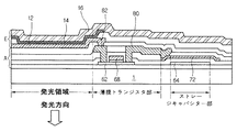
図1は、従来の下部発光方式有機電界発光素子に関する概略的な断面図である。 FIG. 1 is a schematic cross-sectional view of a conventional bottom emission type organic electroluminescence device.
ただし、これは赤、緑、及び青のサブピクセルで構成される一つのピクセル領域を中心にして図示した。 However, this is illustrated centering on one pixel area composed of red, green, and blue sub-pixels.
図示したように、第1、2基板10、30が相互に対向するように配置されており、第1、2基板10、30の縁部はシールパターン40により封じされている。この構造において、第1基板10の透明基板1上部にはサブピクセル別に薄膜トランジスタTが形成され、薄膜トランジスタTと連結されて第1電極12が形成され、薄膜トランジスタT及び第1電極12上部には薄膜トランジスタTと連結されて第1電極12と対応するように配置される赤、緑、及び青のカラーを帯びる発光物質を含む有機電界発光層14が形成され、有機電界発光層14上部には第2電極16が形成されている。
As shown in the figure, the first and
第1、2電極12、16は有機電界発光層14に電界を印加する役割をする。
The first and
そして、前述したシールパターン40によって、第2電極16と第2基板30との間は一定間隔離隔されていて、図面で提示しなかったが、第2基板30の内部面には外部への水分を遮断する吸湿剤及びこの吸湿剤と第2基板30との間を接着するための半透性テープが含まれる。
The
一例として、下部発光方式構造において、第1電極12を陽極で、第2電極16を陰極で構成する場合、第1電極12は透明導電性物質から選択されて、第2電極16は仕事関数が低い金属物質から選択される。こういう条件下で有機電界発光層14は、第1電極12と接する層から正孔注入層14a、正孔輸送層14b、発光層14c、電子輸送層14dが順序通り積層された構造を形成する。
As an example, when the
この時、発光層14cはサブピクセル別に赤、緑、及び青のカラーを具現する発光物質が順序通り配置された構造を有する。
At this time, the
図2は、図1に示した下部発光方式による有機電界発光素子の一つのサブピクセル領域に係る拡大断面図である。 FIG. 2 is an enlarged cross-sectional view of one subpixel region of the organic light emitting device using the bottom emission method shown in FIG.
図示したように、透明基板1上には、半導体層62、ゲート電極68、ソース及びドレイン電極80、82が順序通り形成されて薄膜トランジスタ領域を形成し、ソース電極80には電源供給ライン(図示せず)で形成されたパワー電極72が連結されて、ドレイン電極82には有機電界発光ダイオードEが連結されている。
As shown in the figure, a
そして、パワー電極72と対応する下部には絶縁体が介在した状態で半導体層62と同一物質で構成されたキャパシター電極64が位置して、これらが対応する領域はストレージキャパシター領域を形成する。
A
有機電界発光ダイオードE以外の薄膜トランジスタ領域及びストレージキャパシター領域に形成された素子はアレイ素子Aを形成する。 Elements formed in the thin film transistor region and the storage capacitor region other than the organic electroluminescent diode E form an array device A.
有機電界発光ダイオードEは、有機電界発光層14が介在した状態で相互に対向した第1電極12及び第2電極16で構成される。有機電界発光ダイオードEは自体発光した光を外部に放出させる発光領域に位置する。
The organic electroluminescent diode E is composed of a
このように、既存の有機電界発光素子は、アレイ素子Aと有機電界発光ダイオードEとが同一基板上に積層された構造で形成されることを特徴とした。 As described above, the existing organic electroluminescence device is characterized in that the array device A and the organic electroluminescence diode E are formed on the same substrate.
このように、既存の下部発光方式による有機電界発光素子は、アレイ素子及び有機電界発光ダイオードが形成された基板と別途のカプセル封じ用基板の合着を介して素子を製作した。 As described above, the existing organic light emitting device using the lower light emission method is manufactured through bonding of the substrate on which the array device and the organic light emitting diode are formed and a separate encapsulation substrate.
この場合、アレイ素子の収率と有機電界発光ダイオードの収率との積が有機電界発光素子の収率を決定するため、既存の有機電界発光素子構造では、後半工程に該当する有機電界発光ダイオード工程により、全体工程収率が大きく制限される問題点があった。例えば、アレイ素子が良好に形成されたとしても、1000Å程度の薄膜を用いる有機電界発光層の形成時に異物やその他の要素により不良が発生するようになれば、有機電界発光素子は不良等級と判定される。 In this case, since the product of the yield of the array element and the yield of the organic electroluminescent diode determines the yield of the organic electroluminescent element, in the existing organic electroluminescent element structure, the organic electroluminescent diode corresponding to the latter process is used. There is a problem that the overall process yield is greatly limited by the process. For example, even if the array element is formed satisfactorily, if an organic electroluminescent layer using a thin film of about 1000 mm is formed due to foreign matter or other elements, the organic electroluminescent element is determined to be defective. Is done.
これによって、良品のアレイ素子を製造することに必要とした諸般経費及び材料費損失が招来されて、生産収率が低下する問題点があった。 As a result, various costs and material cost loss required for manufacturing a non-defective array element are incurred, resulting in a problem that the production yield is lowered.
そして、下部発光方式はカプセル封じによる安定性及び工程の自由度が高い反面、開口率の制限があって高解像度製品に適用するに難しい問題点があるが、上部発光方式は薄膜トランジスタ設計が容易で開口率向上が可能であるため製品寿命側面で有利である。しかし、既存の上部発光方式構造では有機電界発光層上部に通常的に陰極が位置することによって材料選択幅が狭いため透過度が制限されて光効率が低下する問題と、光透過度の低下を最少化するために薄膜型保護膜を構成する場合に外気を十分に遮断することができない問題とがある。 The lower light emission method has high stability and high degree of freedom in the process of encapsulation, but there is a problem that the upper light emission method is difficult to apply to high resolution products due to the limited aperture ratio. The aperture ratio can be improved, which is advantageous in terms of product life. However, in the existing upper light emitting structure, the material selection width is narrow because the cathode is usually positioned above the organic electroluminescent layer, so that the transmittance is limited and the light efficiency is lowered. There is a problem that the outside air cannot be sufficiently blocked when a thin film type protective film is formed in order to minimize it.
本発明は、アレイ素子と有機電界発光ダイオードを相異なる基板に構成することであって、第2基板には有機電界発光層を含んだ有機電界発光ダイオードを形成して、第1基板には前記有機電界発光ダイオードを駆動させるための薄膜トランジスタが含まれたアレイ素子を形成し、この薄膜トランジスタ及び有機電界発光ダイオードを電気的に連結させる伝導性スペーサーが第2基板上に形成されることによって、開口率及び解像度を向上させる有機電界発光素子及び製造方法を提供することにその目的がある。 The present invention is to configure the array element and the organic electroluminescent diode on different substrates, wherein the organic electroluminescent diode including an organic electroluminescent layer is formed on the second substrate, and the first substrate is provided with the above-mentioned organic electroluminescent diode. An array element including a thin film transistor for driving the organic electroluminescent diode is formed, and a conductive spacer for electrically connecting the thin film transistor and the organic electroluminescent diode is formed on the second substrate, thereby providing an aperture ratio. An object of the present invention is to provide an organic electroluminescent device and a manufacturing method that improve the resolution.
上記目的を達成するために、本発明の実施形態による有機電界発光素子は、画像が具現される表示領域と表示領域外郭部の非表示領域とに分けられて、表示領域内にサブピクセルが定義されており、一定間隔離隔されて配置された第1、2基板と、第1基板の表示領域内にサブピクセル単位で形成された少なくとも一つの薄膜トランジスタを有するアレイ素子と、第2基板内部面に位置する第1電極と、第1電極上部の各サブピクセルの発光領域を区画する所定領域に形成されたバッファー及びこのバッファー上に形成された隔壁と、各サブピクセルの発光領域内に形成された絶縁層及びこの絶縁層上に形成されたスペーサーと、絶縁層及びスペーサーを含んだ各サブピクセルの発光領域に形成される有機電界発光層と、有機電界発光層が形成された第2基板上に形成される第2電極とを含んでいることを特徴とする。 In order to achieve the above object, the organic electroluminescent device according to an embodiment of the present invention is divided into a display area in which an image is embodied and a non-display area in the outer area of the display area, and sub-pixels are defined in the display area. The first and second substrates spaced apart from each other, an array element having at least one thin film transistor formed in subpixel units in the display area of the first substrate, and an inner surface of the second substrate. A first electrode that is positioned; a buffer formed in a predetermined region that partitions a light emitting region of each subpixel above the first electrode; a partition formed on the buffer; and a light emitting region formed in each subpixel. An insulating layer, a spacer formed on the insulating layer, an organic electroluminescent layer formed in a light emitting region of each subpixel including the insulating layer and the spacer, and an organic electroluminescent layer are formed. Characterized in that and a second electrode formed on the second substrate that is.
また、本発明の実施形態による有機電界発光素子製造方法は、第1基板の表示領域内部面にサブピクセル単位で形成された少なくとも一つの薄膜トランジスタを有するアレイ素子が形成される段階と、第2基板の表示領域上に第1電極が形成される段階と、第1電極上部領域のうち各サブピクセルの発光領域を区画するバッファー及び各サブピクセルの発光領域内の所定領域に絶縁層が形成される段階と、バッファー上の所定領域及び絶縁層上の所定領域にそれぞれ隔壁及びスペーサーが形成される段階と、絶縁層及びスペーサーを含んだ各サブピクセルの発光領域に有機電界発光層が形成される段階と、有機電界発光層が形成された第2基板上に第2電極が形成される段階と、第1基板及び第2基板の縁部にシールパターンが形成されて第1基板及び第2基板が封じされる段階とが含まれることを特徴とする。 In addition, the method for manufacturing an organic light emitting device according to an embodiment of the present invention includes a step of forming an array device having at least one thin film transistor formed in sub-pixel units on an inner surface of a display area of a first substrate, and a second substrate. Forming a first electrode on the display region, a buffer for partitioning a light emitting region of each subpixel in an upper region of the first electrode, and an insulating layer in a predetermined region in the light emitting region of each subpixel. A step of forming a barrier rib and a spacer in a predetermined region on the buffer and a predetermined region on the insulating layer, and a step of forming an organic electroluminescent layer in a light emitting region of each subpixel including the insulating layer and the spacer. A second electrode is formed on the second substrate on which the organic electroluminescent layer is formed, and a seal pattern is formed on the edges of the first substrate and the second substrate. Substrate and the second substrate is characterized to include the steps to be sealed.
以上の説明のように、本発明による有機電界発光素子及びその製造方法によれば、第一に、生産収率及び生産管理効率を向上させることができて、第二に、上部発光方式であるため薄膜トランジスタ設計が容易になって高開口率/高解像度具現が可能であり、第三に、基板上に有機電界発光ダイオード用電極を構成するため、材料選択幅を広げることができ、第四に、上部発光方式でありながらカプセル封じ構造であるため、外気から安定的な製品を提供することができるという長所がある。 As described above, according to the organic electroluminescent device and the manufacturing method thereof according to the present invention, firstly, the production yield and the production management efficiency can be improved, and secondly, the upper light emitting method. Therefore, the thin film transistor can be easily designed, and a high aperture ratio / high resolution can be realized. Third, since the electrode for the organic light emitting diode is formed on the substrate, the material selection range can be expanded. In addition, since it has an encapsulated structure in spite of the upper light emission method, it has an advantage that a stable product can be provided from the outside air.
また、アレイ領域外部からシールパターンまでの領域にダミースペーサーを形成することによって、上下基板間の間隔をアレイ領域内部とほとんど同様であるように維持することができるという長所がある。 Further, by forming a dummy spacer in the region from the outside of the array region to the seal pattern, there is an advantage that the distance between the upper and lower substrates can be maintained almost the same as the inside of the array region.
以下、添付した図面を参照して本発明の実施形態をさらに詳細に説明する。 Hereinafter, embodiments of the present invention will be described in detail with reference to the accompanying drawings.
図3は、本発明の実施形態によるデュアルパネルタイプの有機電界発光素子の概略的な断面図である。 FIG. 3 is a schematic cross-sectional view of a dual panel type organic electroluminescent device according to an embodiment of the present invention.
図3に示したように、相互に一定間隔離隔されて第1及び第2基板110、130が配置されていて、第1基板110の透明基板100内部面にはアレイ素子120が形成されていて、第2基板130の透明基板101内部面には有機電界発光ダイオード素子Eが形成されており、第1及び2基板110、130の縁部はシールパターン140により封じされている。
As shown in FIG. 3, the first and
また、これは、アレイ素子及び有機電界発光ダイオードが形成されて光が発光する表示領域と、表示領域の外郭領域である非表示領域とに分けられる。先ず、表示領域の構成について説明すると次のようである。 In addition, this is divided into a display area where light is emitted by forming an array element and an organic electroluminescence diode, and a non-display area which is an outer area of the display area. First, the configuration of the display area will be described as follows.
有機電界発光ダイオードEには、共通電極として利用される第1電極132と、第1電極132上部面における各サブピクセルの境界部に位置する隔壁135と、隔壁135内領域の有機電界発光層137及び第2電極138が順序通りサブピクセル単位で分離されたパターンで形成されている。
The organic electroluminescent diode E includes a
また、各サブピクセル内に形成される有機電界発光層137の区画、すなわち、発光領域を限定するためにバッファー133が形成される。
In addition, a
隔壁135は、隣接する各サブピクセルを分離する役割を遂行することであって、図示したようにバッファー133上に逆テーパー形状で形成される。
The
また、本発明は、バッファー133が形成される時、発光領域内にバッファーと同一な材料で構成された絶縁層134がさらに形成されて、絶縁層上に隔壁135が形成される時、それと同一な材料で構成されたスペーサー136がさらに形成されることを特徴とする。ここで、バッファー133及び隔壁135は有機質材料または無機質材料で形成されることが望ましい。
In addition, according to the present invention, when the
この時、スペーサー136は、隔壁135とは違って、後に行われる第2電極成膜時においてスペーサー136により切断が発生しないように正テーパー形状に形成することが望ましく、その高さは隔壁135の高さより高く形成する。
At this time, unlike the
すなわち、スペーサー135の外部面が後に形成される有機電界発光層137及び第2電極138により順次覆われるようになって、これによりスペーサー136は伝導性を有するようになって、結果的に第1基板上に形成される各サブピクセルの薄膜トランジスタTと、第2基板上に各サブピクセル別に形成される第2電極138とを電気的に連結させる役割を遂行するようになる。
That is, the outer surface of the
有機電界発光層137は、第1キャリア伝達層137a、発光層137b、及び第2キャリア伝達層137cが順序通り積層された構造で形成されており、第1、2キャリア伝達層137a、137cは発光層137bに電子または正孔を注入及び輸送する役割をする。
The
第1、2キャリア伝達層137a、137cは、陽極及び陰極の配置構造によって決まるものである。例えば、発光層137bが高分子物質から選択されて、第1電極132を陽極、第2電極138を陰極で構成する場合には、第1電極132と連接する第1キャリア伝達層137aは、正孔注入層と正孔輸送層とが順序通り積層された構造を形成して、第2電極138と連接する第2キャリア伝達層137cは、電子注入層と電子輸送層とが順序通り積層された構造で形成される。
The first and second
また、有機電界発光層137は、高分子物質または低分子物質で形成することができるが、低分子物質で形成する場合には真空蒸着法を介して形成され、高分子物質で形成する場合にはインクジェット方法を介して形成される。
The
そして、アレイ素子120は、薄膜トランジスタTを含む素子で、有機電界発光ダイオードEに電流を供給するために、サブピクセル単位で第2電極138と薄膜トランジスタTとを連結する位置に、第2基板上で形成された伝導性スペーサー150が位置する。
The
伝導性スペーサー150は、先に説明したように第2基板の発光領域上の絶縁層134上部に形成されたスペーサー136外部面に第2電極138が覆われるように形成されて伝導性を帯びるようになったものである。これは一般的な液晶表示装置用スペーサーと違って、セルギャップ維持機能より両基板を電気的に連結させることを主目的にする。
As described above, the
すなわち、伝導性スペーサー150は、第1基板110にサブピクセル単位で具備された薄膜トランジスタTのドレイン電極112と、第2基板130に具備された第2電極138とを電気的に連結する役割を遂行するものであって、隔壁135と同一な材料である有機絶縁膜などに形成された柱状のスペーサー136に金属、すなわち、第2電極138がコーティングされたものである。これは第1、2基板110、130のピクセルを1対1に合着して電流を通じるようにする役割をする。
That is, the
本発明は、スペーサー136が第2基板に具備された各サブピクセルの発光領域上に形成されて、スペーサー136の外部面が有機電界発光層137を形成する高分子または低分子物質、及び第2電極138物質により順次覆われて伝導性を帯びるようになるという点でその特徴がある。
In the present invention, the
伝導性スペーサー150と薄膜トランジスタTとの連結部位をさらに詳細に説明すると、薄膜トランジスタTを覆う領域にドレイン電極112を一部露出させるドレインコンタクトホールを有する保護層124が形成されていて、保護層124上部にはドレインコンタクトホールを介してドレイン電極112と連結されるように構成された電気的連結パターン114が形成される。
The connection portion between the
ここで、伝導性スペーサー150は電気的連結パターン114と電気的に接触するようになって、これを通じて結果的に、各サブピクセルに対応する第1基板上の薄膜トランジスタTと、第2基板上の第2電極138とが電気的に連結される。
Here, the
ここで、薄膜トランジスタTは、有機電界発光ダイオードEと連結される駆動用薄膜トランジスタに該当する。 Here, the thin film transistor T corresponds to a driving thin film transistor connected to the organic electroluminescent diode E.
伝導性スペーサー150の外部を形成する金属、すなわち、第2電極138は、伝導性物質から選択され、好ましくは軟性を帯びて抵抗率の値が小さい金属物質から選択されることが望ましい。
The metal that forms the outside of the
そして、有機電界発光層137で発光した光を第2基板130側に発光させる上部発光方式であることを特徴とする。
And, it is an upper light emission method in which the light emitted from the
これにより、第1電極132は透光性を有する導電性物質から選択されることを特徴として、前記第2電極138は不透明金属物質から選択されることが望ましい。
Accordingly, the
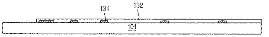
第1電極132を形成する透光性の導電性物質としてはITOが利用されることが望ましいが、ITOは金属自らの抵抗値が高いので、本発明においては、第1電極下部に第1電極の抵抗を小さくするための補助電極131がさらに形成されることを特徴とする。
ITO is preferably used as the light-transmitting conductive material forming the
この時、補助電極131は抵抗率の値が小さい有色の金属で構成することができる。これは図示したように第1基板上に薄膜トランジスタが形成されている領域と対応する領域、すなわち、バッファー133形成領域下部に形成されることが望ましい。
At this time, the
また、第1、2基板110、130間の離隔空間Iには、非活性気体または絶縁性液体が詰められることができる。
Further, the separation space I between the first and
図面で提示しなかったが、アレイ素子120は、走査線と走査線とが交差し、相互に一定間隔離隔される信号線及び電力供給線と、走査線と信号線とが交差する地点に位置するスイッチング薄膜トランジスタ、及びストレージキャパシターとをさらに含む。
Although not shown in the drawing, the
次に、本発明の実施形態による有機電界発光素子の非表示領域について説明する。図示したように、非表示領域には表示領域の最外郭サブピクセルに隣接して形成された複数のダミーサブピクセルと、第1基板110から共通電圧の印加を受けるために第2基板130上に形成された共通電極としての第1電極132とに伝達するための共通電極連結部170、及び共通電極連結部170でシールパターン140までの領域に複数形成されたダミースペーサー160が具備される。
Next, the non-display area of the organic electroluminescence device according to the embodiment of the present invention will be described. As shown in the drawing, the non-display area includes a plurality of dummy sub-pixels formed adjacent to the outermost sub-pixel of the display area and the second substrate 130 to receive a common voltage from the
このようなデュアルパネルタイプの有機電界発光素子は、アレイ素子と有機電界発光ダイオード素子とをそれぞれ相異なる基板上に構成するため、既存のアレイ素子と有機電界発光ダイオード素子とを同一基板上に形成する場合と比較する時、アレイ素子の収率に有機電界発光ダイオード素子が影響を受けることがないため、各素子の生産管理側面でも養護な特性を示すことができる。 In such a dual panel type organic electroluminescent element, the array element and the organic electroluminescent diode element are formed on different substrates, so the existing array element and the organic electroluminescent diode element are formed on the same substrate. When compared with the case where the organic electroluminescent diode element is not affected by the yield of the array element, it is possible to show protective characteristics in terms of production control of each element.
また、前述した条件下において上部発光方式へ画面を具現するようになれば、開口率を念頭に置かずに薄膜トランジスタを設計することができてアレイ工程効率を高めることができて、高開口率/高解像度製品を提供することができ、デュアルパネルタイプで有機電界発光ダイオード素子を形成するため、既存の上部発光方式より外気を效果的に遮断することができて製品の安全性を高めることができる。 In addition, if the screen is implemented in the upper light-emitting method under the above-described conditions, the thin film transistor can be designed without considering the aperture ratio, and the array process efficiency can be increased. High-resolution products can be provided, and the organic electroluminescence diode element is formed in a dual panel type, so that the outside air can be effectively blocked from the existing upper light emitting method, and the safety of the product can be improved. .
また、従来の下部発光方式製品で発生した薄膜トランジスタ設計に対しても、有機電界発光ダイオード素子と別途の基板に構成するによって、薄膜トランジスタ配置に対する自由度を十分に得ることができて、有機電界発光ダイオード素子の第1電極を透明基板上に形成するため、既存のアレイ素子上部に第1電極を形成する構造と比較してみる時、第1電極に対する自由度を高めることができる長所を有するようになる。 In addition, even for thin film transistor designs generated in conventional lower light emission type products, organic EL devices can be obtained with sufficient freedom by arranging the organic EL devices on a separate substrate. Since the first electrode of the element is formed on the transparent substrate, it has an advantage that the degree of freedom with respect to the first electrode can be increased when compared with a structure in which the first electrode is formed on the existing array element. Become.
図4は、図3の特定領域Aに対する詳細断面図で、これは本発明の実施形態によるデュアルパネルタイプの有機電界発光素子において、第2基板130の表示領域上に形成された一つのサブピクセル領域を示すものである。 FIG. 4 is a detailed cross-sectional view illustrating a specific area A of FIG. 3, which is a sub-pixel formed on the display area of the second substrate 130 in the dual panel type organic electroluminescent device according to an embodiment of the present invention. Indicates the area.
図4を参照すると、第2基板130は、透明基板101上に第1電極132が形成されて、第1電極132の上部面に各サブピクセルの境界部に位置するバッファー133及び隔壁135が形成されている。
Referring to FIG. 4, in the second substrate 130, the
バッファー133は、各サブピクセル内に形成される有機電界発光層137を区画、すなわち、発光領域を限定する役割をしている。隔壁135は、隣接する各サブピクセルを分離する役割を遂行するものであって、図示したようにバッファー133上に逆テーパー形状で形成される。
The
すなわち、各サブピクセルは、バッファー133内の領域を発光領域にして、この領域に有機電界発光層を形成する高分子または低分子物質が形成されるものである。
That is, each subpixel has a region in the
本発明は、発光領域内にバッファー133が形成される時、バッファーと同一な材料で構成された絶縁層134がさらに形成されて、絶縁層134上に隔壁135が形成される時、それと同一な材料で構成されたスペーサー136がさらに形成されることを特徴とする。
In the present invention, when the
ここで、バッファー133及び隔壁135は有機質材料または無機質材料で形成されることが望ましく、スペーサー136は隔壁135とは違って後に行われる第2電極138成膜時においてスペーサー136により切断が発生しないように正テーパー形状に形成することが望ましく、その高さは隔壁135の高さより高く形成する。
Here, the
すなわち、スペーサー136の外部面は後に形成される有機電界発光層137及び第2電極138により順次覆われるようになって、これによりスペーサー136は伝導性を有するようになって、結果的に、第1基板上に形成される各サブピクセルの薄膜トランジスタと、第2基板上に各サブピクセル別に形成される第2電極とを電気的に連結させる役割を遂行するようになる。
That is, the outer surface of the
伝導性スペーサー150は、発光領域上の絶縁層134上部に形成されたスペーサー136外部面に第2電極138が覆われるように形成されて伝導性を帯びるようになったものである。これは一般的な液晶表示装置用スペーサーと違って、セルギャップ維持機能より両基板を電気的に連結させることを主目的にする。
The
すなわち、伝導性スペーサー150は、第1基板にサブピクセル単位で具備された薄膜トランジスタTのドレイン電極と、第2基板130に具備された第2電極138とを電気的に連結する役割を遂行するものであって、隔壁と同一な材料である有機絶縁膜などに形成された柱状のスペーサーに金属、すなわち、第2電極138がコーティングされたものである。これは第1、2基板110、130のピクセルを1対1に合着して電流を通じるようにする役割をする。
That is, the
本発明は、スペーサー136が第2基板130に具備された各サブピクセルの発光領域上に形成されて、スペーサー136の外部面が有機電界発光層137を形成する高分子または低分子物質、及び第2電極物質により順次覆われて伝導性を帯びるようになるという点でその特徴がある。
In the present invention, the
また、有機電界発光層137は、第1キャリア伝達層、発光層、及び第2キャリア伝達層が順序通り積層された構造で形成されており、第1、2キャリア伝達層は発光層に電子または正孔を注入及び輸送する役割をする。
The
有機電界発光層137は、高分子物質または低分子物質で形成することができるが、低分子物質で形成する場合には真空蒸着法を介して形成して、高分子物質で形成する場合にはインクジェット法を介して形成する。
The
また、有機電界発光層137上部に形成される第2電極138は、伝導性スペーサー150の最外郭を覆うように形成されるが、これは伝導性物質から選択され、好ましくは軟性を帯びて、抵抗率値が低い金属物質から選択されることが望ましい。
In addition, the
そして、有機電界発光層137で発光した光は上部方向に発光するため、第1電極132は透光性を有する導電性物質から選択されることを特徴として、第2電極138は不透明金属物質から選択されることが望ましい。
Since the light emitted from the
第1電極を形成する透光性の導電性物質としてはITOが利用されることが望ましいが、ITOは金属自らの抵抗値が高いので、本発明においては、第1電極下部に第1電極の抵抗を小さくするための補助電極131がさらに形成されることを特徴とする。
ITO is preferably used as the translucent conductive material forming the first electrode. However, since ITO has a high resistance value of the metal itself, in the present invention, the first electrode is disposed under the first electrode. An
この時、補助電極131は抵抗率の値が小さい有色の金属で構成することができる。これは図示したように第1基板上に薄膜トランジスタが形成された領域と対応する領域、すなわち、バッファー133形成領域下部に形成されることが望ましい。
At this time, the
図5は、図3に示した有機電界発光素子の外郭領域に対応する詳細断面図である。 FIG. 5 is a detailed cross-sectional view corresponding to the outer region of the organic electroluminescent device shown in FIG.
図5を参照すると、有機電界発光ダイオード及びアレイ素子が形成された表示領域外部の非表示領域には、表示領域の最外郭サブピクセルに隣接して形成された複数のダミーサブピクセルと、第1基板から共通電圧の印加を受けるために第2基板上に形成された共通電極としての第1電極132に伝達するための共通電極連結部170、及び共通電極連結部170からシールパターン140までの領域に複数形成されたダミースペーサー160が具備される。
Referring to FIG. 5, the non-display area outside the display area where the organic light emitting diode and the array element are formed includes a plurality of dummy sub-pixels formed adjacent to the outermost sub-pixel of the display area, Common
ここで、ダミーサブピクセルは、第2基板上の表示領域内に形成されたサブピクセルとは違って、発光領域内に絶縁層及びスペーサーが形成されないため、これに対応する第1基板上の領域に薄膜トランジスタが形成されず、所定の信号の提供を受けることができない。 Here, unlike the sub-pixel formed in the display area on the second substrate, the dummy sub-pixel is not formed with an insulating layer and a spacer in the light-emitting area, and thus corresponds to the area on the first substrate. A thin film transistor is not formed on the substrate, and a predetermined signal cannot be provided.
また、共通電極連結部170は、第2基板上に形成された第1電極132の終端部上に形成された絶縁層134及びスペーサー136に、第2電極138を形成する金属が覆われることで形成されるものであって、これは第1基板の一面に具備された電極パッド180と電気的に連結される。
Further, the common
第1電極132は、共通電極の役割をするものであって、常に一定な電圧が印加されなければならないが、図示したように共通電圧は第1基板の一面に具備された電極パッド180から印加されて第1電極に入力される。
The
すなわち、電極パッド180から印加された電圧は、第1電極132の終端部に形成された共通電極連結部170を介して、第1電極132に印加される。
That is, the voltage applied from the
また、表示領域に対しては、伝導性スペーサー(図4の150)がサブピクセル領域毎に個別的に形成されていて一定なギャップを形成する役割をして、両基板の縁に形成されたシールパターン140内部にガラス繊維が具備されて所定の間隔を維持するようにするが、大面積の有機電界発光素子の場合には、第1、2基板間の間隔を一定に維持することが容易ではない。
Also, for the display area, conductive spacers (150 in FIG. 4) are individually formed for each sub-pixel area to form a constant gap, and are formed on the edges of both substrates. Glass fibers are provided inside the
本発明は、問題を克服するために共通電極連結部170からシールパターン140までの領域に複数のダミースペーサー160を具備し、これを通じて第1、2基板すなわち、上、下基板の間隔を表示領域内部とほとんど同様であるように維持することができるようになる。
In order to overcome the problem, the present invention includes a plurality of
すなわち、大面積の有機電界発光素子パネルを形成するようになっても、従来のようなディスプレー不良は発生しない。 That is, even when an organic electroluminescent element panel having a large area is formed, a conventional display defect does not occur.
この時、ダミースペーサー160は、表示領域上で絶縁層及びスペーサーが形成される時に、第1電極が形成されない第2基板上に形成される。
At this time, the
図6A〜図6Fは、本発明による有機電界発光素子の製造工程を示す工程断面図である。ただし、これは図3に示した断面図を中心にして図示したものである。 6A to 6F are process cross-sectional views illustrating a manufacturing process of an organic electroluminescent device according to the present invention. However, this is illustrated with the cross-sectional view shown in FIG. 3 as the center.
まず図6Aを参照すると、第1基板上の表示領域にアレイ素子120が形成されている。
First, referring to FIG. 6A, an
例えば、アレイ素子120を構成する薄膜トランジスタTが図示したようにポリシリコーン薄膜トランジスタである場合、上記段階は、透明基板100上にバッファー層を形成する段階と、バッファー層上部に半導体層及びキャパシター電極を形成する段階と、半導体層上部にゲート電極、ソース及びドレイン電極を形成する段階と、キャパシター電極上部に位置して、ソース電極と連結されるパワー電極を形成する段階とを含む。
For example, when the thin film transistor T constituting the
また、アレイ素子120が形成されると、このアレイ素子120に具備された駆動薄膜トランジスタTのドレイン電極112と電気的に連結される電気的連結パターン114が形成される。
When the
電気的連結パターン114と駆動薄膜トランジスタTとの連結部位をさらに詳細に説明する。薄膜トランジスタTを覆う領域にドレイン電極112を一部露出させるドレインコンタクトホールを有する保護層124が形成され、この保護層124上部にはドレインコンタクトホールを介してドレイン電極112と連結されて電気的連結パターン114が位置する。電気的連結パターン114は、後に第2基板上に形成される伝導性スペーサーと接触して結果的に第1基板と第2基板を電気的に連結する役割をするようになる。
A connection portion between the
ただし、電気的連結パターン114はドレイン電極112と一体型に形成されることができる。
However, the
また、電気的連結パターン114が形成される時、第1基板の非表示領域上には電気的連結パターン114のような金属材質の電極パッド180が形成される。
Further, when the
次に図6Bに示したように、第2基板の透明基板101上に有機電界発光ダイオードの第1電極132が形成される。
Next, as shown in FIG. 6B, the
この時、第1電極132は透明導電物質であるITO電極が使われることが望ましい。
At this time, the
ただし、ITOは金属自らの抵抗値が高いので、本発明においては、第1電極下部に第1電極の抵抗を小さくするための補助電極131がさらに形成されることを特徴とする。
However, since ITO has a high resistance value of the metal itself, the present invention is characterized in that an
この時、補助電極131は、抵抗率の値が小さい有色の金属で構成することができる。これは図示したように、第1基板上に薄膜トランジスタが形成された領域と対応する領域、すなわち、今後形成されるバッファー形成領域下部に形成されることが望ましい。
At this time, the
次に図6Cに示したように、表示領域の場合、第1電極の上部の所定領域、すなわち、各サブピクセルを区画するサブピクセルの外郭領域にバッファー133が形成されて、バッファー133が形成された領域上に隔壁135が形成され、発光領域内にバッファーと同一な材料で構成された絶縁層134が形成されて、絶縁層上に隔壁と同一な材料で構成されたスペーサー136が形成される。
Next, as shown in FIG. 6C, in the case of the display region, the
バッファー133は、各サブピクセル内に形成される有機電界発光層の区画、すなわち、発光領域を限定する役割をしており、隔壁135は、隣接する各サブピクセルを分離する役割を遂行するものであって、図示したように、バッファー133上に逆テーパー形状で形成される。
The
これに反して、スペーサー136は、隔壁とは違って後に行われる第2電極成膜時においてスペーサー136により切断が発生しないように正テーパー形状に形成することが望ましく、その高さは隔壁135の高さより高く形成する。
Contrary to this, unlike the partition, the
また、非表示領域では、第1電極132の終端部に後に共通電極連結部を形成する絶縁層134及びスペーサー136が形成されて、第1電極が形成されない第2基板上の領域にも絶縁層134及びスペーサー136が形成されて、ダミースペーサー160を形成する。
In the non-display region, an insulating
次に図6Dに示したように、有機電界発光層137が各サブピクセルにおいてバッファー133により定義された領域内で形成される。
Next, as shown in FIG. 6D, an
ここで、有機電界発光層137は、高分子または低分子物質で形成されることを特徴としており、第1電極が陽極、第2電極が陰極と仮定する場合、正孔伝達層137a、発光層137b、及び電子伝達層137cが順序通り積層された構造で形成されており、正孔/電子伝達層137a、137cは発光層137bに正孔または電子を注入及び輸送する役割をする。ただし、有機電界発光層137は低分子物質で形成されることができる。
Here, the
この時、第1電極と連接する正孔伝達層137aは、正孔注入層及び正孔輸送層が順序通り積層された構造を形成して、今後第2電極と連接する諸電子伝達層137cは、電子注入層及び電子輸送層が順序通り積層された構造で構成されることができる。
At this time, the
このように、有機電界発光層137がバッファー133内領域に形成されると、図6Eに示したように、その上部に有機電界発光ダイオードの第2電極138が形成される。
When the
第2電極138は、隔壁135により各サブピクセル別に分けられるので結果的に画素電極の役割を遂行するようになる。
Since the
このように、発光領域内に有機電界発光層137及び第2電極138が形成されると、発光領域内に具備されたスペーサー136の外部面は有機電界発光層137及び第2電極138により順次覆われる。
As described above, when the
これにより、スペーサー136は、伝導性を有するようになって結果的に第1基板上に形成される各サブピクセルの薄膜トランジスタと、第2基板上に各サブピクセル別に形成される第2電極とを電気的に連結させる役割を遂行するようになる。
Accordingly, the
伝導性スペーサー150は、発光領域上の絶縁層134上部に形成されたスペーサー136外部面に第2電極138が覆われるように形成されて伝導性を帯びるようになったものである。これは一般的な液晶表示装置用スペーサーと違って、セルギャップ維持機能より、両基板を電気的に連結させることを主目的にする。
The
すなわち、伝導性スペーサー150は、第1基板110にサブピクセル単位で具備された薄膜トランジスタTのドレイン電極112と、第2基板130に具備された第2電極138とを電気的に連結する役割を遂行するものであって、隔壁と同一な材料である有機絶縁膜などに形成された柱状のスペーサーに金属、すなわち、第2電極がコーティングされたものである。これは、第1、2基板110、130のピクセルを1対1に合着して電流を通じるようにする役割をする。
That is, the
また、非表示領域上の第1電極終端部に形成された絶縁層134及びスペーサー136を覆うように第2電極138が形成されて、これが第1基板上に形成された電極パッド180と接触されることによって、これは共通電極連結部170となる。
Further, a
次に図6Fに示したように、第1、2基板110、130を合着して、カプセル封じするようになれば、第1基板110の電気的連結パターン114と第2基板130の伝導性スペーサー150とが相互に接触されることにより、第1、2基板110、130が相互に電気的に連結しており、これは結果的に第2基板130上に形成された有機電界発光ダイオードの第2電極138と、第1基板110上に形成された駆動薄膜トランジスタTのドレイン電極112とが電気的に連結される。
Next, as shown in FIG. 6F, when the first and
131:補助電極
132:第1電極
133:バッファー
134:絶縁層
135:隔壁
136:スペーサー
137:有機電界発光層
138:第2電極
150:伝導性スペーサー
160:ダミースペーサー
170:共通電極連結部
131: auxiliary electrode 132: first electrode 133: buffer 134: insulating layer 135: partition wall 136: spacer 137: organic electroluminescent layer 138: second electrode 150: conductive spacer 160: dummy spacer 170: common electrode connecting portion
Claims (21)
前記第1基板の表示領域内にサブピクセル単位で形成された少なくとも一つの薄膜トランジスタを有するアレイ素子と、
前記第2基板内部面に位置する第1電極と、
前記第1電極上部の各サブピクセルの発光領域を区画する所定領域に形成されたバッファー及び該バッファー上に形成された隔壁と、
前記各サブピクセルの発光領域内に形成された絶縁層と、
前記絶縁層及びスペーサーを含んだ各サブピクセルの発光領域に形成される有機電界発光層と、
前記絶縁層上に形成されるスペーサーと、
前記発光領域及び前記スペーサー上に形成される第2電極と、
前記第1電極下部に、前記第1電極の抵抗を小さくするための補助電極を含み、
前記スペーサー上の前記第2電極は、各サブピクセルの前記第1基板の前記表示領域における前記薄膜トランジスタのドレイン電極に電気的に接触し、
前記スペーサーは、テーパー形状を有し、前記有機電界発光層及び前記第2電極で覆われ、
前記スペーサー上の前記第2電極は、前記アレイ素子と電気的に接続され、
前記非表示領域には、
前記表示領域の最外郭サブピクセルに隣接して形成された複数のダミーサブピクセルと、
前記第1基板から共通電圧の印加を受け、前記第1電極へ共通電圧を伝達するための共通電極連結部と、ここで、前記第1電極は前記第2基板上に形成された共通電極として機能し、前記共通電極連結部は前記第1電極の終端部に形成された第2スペーサーと、前記第2スペーサーを覆い前記第2電極と同じ金属で作られた金属層を含み、
前記基板の縁部に形成され、前記第1及び第2基板を封じするシールパターンと、
前記共通電極連結部から前記シールパターンまでの領域の複数のダミースペーサーを含む
ことを特徴とする有機電界発光素子。 The first and second substrates are divided into a display area in which an image is embodied and a non-display area of the outer area of the display area, and subpixels are defined in the display area, and are spaced apart from each other by a certain distance. When,
An array element having at least one thin film transistor formed in sub-pixel units in the display area of the first substrate;
A first electrode located on the inner surface of the second substrate;
A buffer formed in a predetermined region that partitions a light emitting region of each sub-pixel above the first electrode, and a partition formed on the buffer;
An insulating layer formed in the light emitting region of each subpixel;
An organic electroluminescent layer formed in a light emitting region of each subpixel including the insulating layer and a spacer;
A spacer formed on the insulating layer;
A second electrode formed on the light emitting region and the spacer;
An auxiliary electrode for reducing the resistance of the first electrode is included under the first electrode,
The second electrode on the spacer is in electrical contact with a drain electrode of the thin film transistor in the display region of the first substrate of each subpixel;
The spacer has a tapered shape and is covered with the organic electroluminescent layer and the second electrode,
The second electrode on the spacer is electrically connected to the array element ;
In the non-display area,
A plurality of dummy subpixels formed adjacent to the outermost subpixel of the display region;
A common electrode connection part for receiving a common voltage applied from the first substrate and transmitting the common voltage to the first electrode, wherein the first electrode is a common electrode formed on the second substrate; The common electrode connecting portion includes a second spacer formed at a terminal portion of the first electrode, and a metal layer covering the second spacer and made of the same metal as the second electrode;
A seal pattern formed on an edge of the substrate and sealing the first and second substrates;
An organic electroluminescent device comprising a plurality of dummy spacers in a region from the common electrode connecting portion to the seal pattern .
前記第1電極上に補助電極が形成される段階と、
第2基板の表示領域上に第1電極が形成される段階と、
前記第1電極上部領域のうち各サブピクセルの発光領域を区画するバッファー及び前記各サブピクセルの発光領域内の所定領域に絶縁層が形成される段階と、
前記バッファー上の所定領域に隔壁、前記絶縁層上の所定領域にスペーサー、及び前記第1電極の終端部の非表示領域に第2スペーサーが形成される段階と、
前記絶縁層及びスペーサーを含んだ各サブピクセルの発光領域に有機電界発光層が形成される段階と、
前記発光領域及び前記スペーサー上に第2電極が形成される段階と、ここで、前記スペーサー上の前記第2電極は、各サブピクセルの前記第1基板の前記表示領域における前記薄膜トランジスタのドレイン電極に電気的に接触し、
前記第1基板及び第2基板の縁部にシールパターンが形成されて前記第1基板及び第2基板が封じされる段階と、
前記第2基板を同じ金属材料で前記第2スペーサーを覆うことにより共通電極連結部が形成される段階を含み、
前記スペーサーは、テーパー形状を有し、前記有機電界発光層及び前記第2電極で覆われ、
前記補助電極は、前記第1電極の抵抗を小さくするために、前記第1電極の下部に配置され、
前記スペーサー上の前記第2電極は、前記アレイ素子と電気的に接続される
ことを特徴とする有機電界発光素子の製造方法。 Forming an array element having at least one thin film transistor formed in sub-pixel units on the inner surface of the display area of the first substrate;
Forming an auxiliary electrode on the first electrode;
Forming a first electrode on a display area of a second substrate;
A step of forming an insulating layer in a predetermined region in the light emitting region of each subpixel and a buffer that partitions the light emitting region of each subpixel in the first electrode upper region;
Forming a partition in a predetermined region on the buffer, a spacer in a predetermined region on the insulating layer, and a second spacer in a non-display region at a terminal portion of the first electrode ;
Forming an organic electroluminescent layer in a light emitting region of each subpixel including the insulating layer and a spacer;
Forming a second electrode on the light emitting region and the spacer, wherein the second electrode on the spacer is a drain electrode of the thin film transistor in the display region of the first substrate of each subpixel; In electrical contact,
A step of sealing the first substrate and the second substrate by forming a seal pattern on an edge of the first substrate and the second substrate ;
A step of forming a common electrode connection part by covering the second spacer with the same metal material on the second substrate ;
The spacer has a tapered shape and is covered with the organic electroluminescent layer and the second electrode,
The auxiliary electrode is disposed under the first electrode in order to reduce the resistance of the first electrode.
The method of manufacturing an organic electroluminescent element, wherein the second electrode on the spacer is electrically connected to the array element.
Applications Claiming Priority (1)
| Application Number | Priority Date | Filing Date | Title |
|---|---|---|---|
| KR1020040074059A KR100642490B1 (en) | 2004-09-16 | 2004-09-16 | Organic Electro luminescence Device and fabrication method thereof |
Publications (2)
| Publication Number | Publication Date |
|---|---|
| JP2006086504A JP2006086504A (en) | 2006-03-30 |
| JP4397860B2 true JP4397860B2 (en) | 2010-01-13 |
Family
ID=36091606
Family Applications (1)
| Application Number | Title | Priority Date | Filing Date |
|---|---|---|---|
| JP2005191266A Active JP4397860B2 (en) | 2004-09-16 | 2005-06-30 | Organic electroluminescent device and manufacturing method thereof |
Country Status (6)
| Country | Link |
|---|---|
| US (1) | US7948164B2 (en) |
| EP (1) | EP1648032B8 (en) |
| JP (1) | JP4397860B2 (en) |
| KR (1) | KR100642490B1 (en) |
| CN (1) | CN100515152C (en) |
| TW (1) | TWI285516B (en) |
Families Citing this family (46)
| Publication number | Priority date | Publication date | Assignee | Title |
|---|---|---|---|---|
| DE102004031670B4 (en) * | 2003-12-30 | 2011-08-18 | Lg Display Co., Ltd. | Organo-electroluminescent device and manufacturing method thereof |
| KR100720143B1 (en) * | 2005-12-13 | 2007-05-18 | 삼성전자주식회사 | Display device |
| KR101157262B1 (en) | 2005-12-14 | 2012-06-15 | 엘지디스플레이 주식회사 | Organic electro-luminescence display device and method for fabricating of the same |
| US8017950B2 (en) * | 2005-12-29 | 2011-09-13 | Lg Display Co., Ltd. | Organic electro-luminescence display device and method of manfacturing the same |
| KR100647339B1 (en) * | 2006-01-11 | 2006-11-23 | 삼성전자주식회사 | Flat panel display device |
| KR20070090523A (en) * | 2006-03-03 | 2007-09-06 | 삼성전자주식회사 | Display device and manufacturing method of the same |
| TWI307978B (en) * | 2006-04-28 | 2009-03-21 | Au Optronics Corp | Cascade organic electroluminescent device |
| KR100914784B1 (en) * | 2006-05-17 | 2009-08-31 | 엘지디스플레이 주식회사 | Light emitting device and fabrication method of the same |
| US7667386B2 (en) * | 2006-06-21 | 2010-02-23 | Chunghwa Picture Tubes, Ltd. | Fabricating method of display panel |
| KR101241140B1 (en) * | 2006-06-26 | 2013-03-08 | 엘지디스플레이 주식회사 | Shadow mask organic electroluminescent display device using the same and fabricating method thereof |
| KR100713227B1 (en) * | 2006-06-30 | 2007-05-02 | 삼성전자주식회사 | Display device and manufacturing method thereof |
| KR101331801B1 (en) * | 2006-06-30 | 2013-11-21 | 엘지디스플레이 주식회사 | Organic elctroluminescence display device capable of reducing power consumption |
| KR101213103B1 (en) * | 2006-06-30 | 2013-01-09 | 엘지디스플레이 주식회사 | bonding device and fa brication method of Light emitting device using thereof |
| KR101331800B1 (en) * | 2006-06-30 | 2013-11-21 | 엘지디스플레이 주식회사 | Organic electro luminescence display device |
| KR101274807B1 (en) * | 2006-06-30 | 2013-06-13 | 엘지디스플레이 주식회사 | organic electro-luminescence display device and method for fabricating the same |
| KR101192075B1 (en) * | 2006-06-30 | 2012-10-17 | 엘지디스플레이 주식회사 | Method for fabricating of organic electro-luminescence display device |
| KR101281888B1 (en) * | 2006-06-30 | 2013-07-03 | 엘지디스플레이 주식회사 | organic electro-luminescence display device and method for fabricating the same |
| KR101462061B1 (en) * | 2006-09-29 | 2014-11-17 | 가부시키가이샤 한도오따이 에네루기 켄큐쇼 | Semiconductor device |
| KR101291845B1 (en) * | 2006-12-13 | 2013-07-31 | 엘지디스플레이 주식회사 | Organic light emitting diodes display device and method of manufacturing the same |
| CN101232013B (en) * | 2007-01-25 | 2011-03-30 | 奇美电子股份有限公司 | Organic illuminated display element and manufacturing method thereof |
| US8183766B2 (en) | 2007-03-07 | 2012-05-22 | Au Optronics Corp. | Pixel structure of organic electroluminescent display panel and method of making the same |
| WO2009001241A1 (en) * | 2007-06-25 | 2008-12-31 | Koninklijke Philips Electronics N.V. | Organic functional device and method of manufacturing same |
| KR101337188B1 (en) * | 2007-10-25 | 2013-12-05 | 엘지디스플레이 주식회사 | Method of manufacturing organic light emitting diode display device |
| KR100889682B1 (en) | 2008-01-30 | 2009-03-19 | 삼성모바일디스플레이주식회사 | Organic light emitting display and making method for the same |
| US8022621B2 (en) * | 2008-07-31 | 2011-09-20 | Lg Display Co., Ltd. | Organic light emitting display device |
| KR100963075B1 (en) * | 2008-10-29 | 2010-06-14 | 삼성모바일디스플레이주식회사 | Organic light emitting display device |
| KR101107158B1 (en) * | 2009-07-10 | 2012-01-25 | 삼성모바일디스플레이주식회사 | Organic light emitting diode display and method for manufacturing the same |
| CN101866943B (en) * | 2010-02-26 | 2013-12-25 | 信利半导体有限公司 | Organic light-emitting diode display and packaging method thereof |
| KR101258261B1 (en) * | 2010-04-21 | 2013-04-25 | 엘지디스플레이 주식회사 | Organic Light Emitting Display Device |
| EP2592672B1 (en) * | 2010-07-08 | 2021-01-27 | LG Display Co., Ltd. | Organic light-emitting device and method for manufacturing same |
| KR101202352B1 (en) * | 2010-07-19 | 2012-11-16 | 삼성디스플레이 주식회사 | Organic light emitting display device and method for manufacturing the same |
| KR102050505B1 (en) | 2011-02-10 | 2019-11-29 | 가부시키가이샤 한도오따이 에네루기 켄큐쇼 | Light-emitting device and manufacturing method thereof, lighting device, and display device |
| KR20130049728A (en) | 2011-11-04 | 2013-05-14 | 가부시키가이샤 한도오따이 에네루기 켄큐쇼 | Light-emitting module and light-emitting device |
| CN103296056B (en) * | 2012-12-30 | 2015-10-07 | 上海天马微电子有限公司 | Organic LED display device and manufacture method thereof |
| JP6221418B2 (en) | 2013-07-01 | 2017-11-01 | セイコーエプソン株式会社 | LIGHT EMITTING DEVICE AND ELECTRONIC DEVICE |
| KR102081288B1 (en) * | 2013-08-08 | 2020-02-26 | 삼성디스플레이 주식회사 | Organic light emitting display apparatus and method for manufacturing the same |
| TW201526330A (en) * | 2013-09-30 | 2015-07-01 | Lg Chemical Ltd | Organic light emitting device |
| TWI568052B (en) * | 2013-09-30 | 2017-01-21 | 樂金顯示科技股份有限公司 | Method for preparing organic light emitting device |
| TWI583036B (en) * | 2013-09-30 | 2017-05-11 | 樂金顯示科技股份有限公司 | Laminate and method for preparing the same |
| KR102357269B1 (en) * | 2014-12-12 | 2022-02-03 | 삼성디스플레이 주식회사 | Organic light emitting display device and method of manufacturing the same |
| WO2016208430A1 (en) * | 2015-06-26 | 2016-12-29 | Necライティング株式会社 | Organic el device, organic el lighting panel, organic el lighting device, and organic el display |
| JP7236844B2 (en) * | 2018-11-12 | 2023-03-10 | 株式会社ジャパンディスプレイ | Display device and manufacturing method thereof |
| CN109768182B (en) * | 2019-01-23 | 2023-07-28 | 京东方科技集团股份有限公司 | OLED substrate, array substrate, display panel and display device |
| CN110047905B (en) | 2019-05-16 | 2022-08-09 | 京东方科技集团股份有限公司 | Display substrate, display panel and display device |
| KR102427292B1 (en) * | 2021-01-20 | 2022-07-29 | 국방과학연구소 | Method and System for Controlling for Operation of a Robot System |
| CN117643200A (en) * | 2022-06-30 | 2024-03-01 | 京东方科技集团股份有限公司 | Display substrate, display panel and electronic equipment |
Family Cites Families (9)
| Publication number | Priority date | Publication date | Assignee | Title |
|---|---|---|---|---|
| US5294869A (en) * | 1991-12-30 | 1994-03-15 | Eastman Kodak Company | Organic electroluminescent multicolor image display device |
| TW515109B (en) * | 1999-06-28 | 2002-12-21 | Semiconductor Energy Lab | EL display device and electronic device |
| US6548961B2 (en) * | 2001-06-22 | 2003-04-15 | International Business Machines Corporation | Organic light emitting devices |
| KR100710157B1 (en) | 2002-04-04 | 2007-04-20 | 엘지.필립스 엘시디 주식회사 | Liquid Crystal Display Device and Method of manufacturing the same |
| KR100435054B1 (en) | 2002-05-03 | 2004-06-07 | 엘지.필립스 엘시디 주식회사 | The organic electro-luminescence device and method for fabricating of the same |
| KR100473591B1 (en) * | 2002-07-18 | 2005-03-10 | 엘지.필립스 엘시디 주식회사 | Dual Panel Type Organic Electroluminescent Device and Method for Fabricating the same |
| KR100544436B1 (en) * | 2002-11-26 | 2006-01-23 | 엘지.필립스 엘시디 주식회사 | The organic electro-luminescence device and method for fabricating of the same |
| TWI272872B (en) * | 2002-12-13 | 2007-02-01 | Lg Philips Lcd Co Ltd | Dual panel-type organic electroluminescent display device and method of fabricating the same |
| JP2004342432A (en) * | 2003-05-15 | 2004-12-02 | Nec Corp | Organic el (electroluminescence) display device |
-
2004
- 2004-09-16 KR KR1020040074059A patent/KR100642490B1/en active IP Right Grant
-
2005
- 2005-06-29 EP EP05014113A patent/EP1648032B8/en active Active
- 2005-06-30 JP JP2005191266A patent/JP4397860B2/en active Active
- 2005-06-30 US US11/170,073 patent/US7948164B2/en active Active
- 2005-06-30 CN CNB2005100801886A patent/CN100515152C/en active Active
- 2005-06-30 TW TW094122143A patent/TWI285516B/en active
Also Published As
| Publication number | Publication date |
|---|---|
| EP1648032A2 (en) | 2006-04-19 |
| TW200611601A (en) | 2006-04-01 |
| CN1750720A (en) | 2006-03-22 |
| US7948164B2 (en) | 2011-05-24 |
| EP1648032B8 (en) | 2012-09-19 |
| KR100642490B1 (en) | 2006-11-02 |
| TWI285516B (en) | 2007-08-11 |
| JP2006086504A (en) | 2006-03-30 |
| EP1648032A3 (en) | 2010-06-30 |
| CN100515152C (en) | 2009-07-15 |
| KR20060025317A (en) | 2006-03-21 |
| EP1648032B1 (en) | 2012-08-08 |
| US20060055313A1 (en) | 2006-03-16 |
Similar Documents
| Publication | Publication Date | Title |
|---|---|---|
| JP4397860B2 (en) | Organic electroluminescent device and manufacturing method thereof | |
| JP4324131B2 (en) | Organic electroluminescent device and manufacturing method thereof | |
| US11825716B2 (en) | Display device | |
| KR100642491B1 (en) | Organic Electro luminescence Device | |
| JP4365364B2 (en) | Organic electroluminescent device and manufacturing method thereof | |
| KR20040037623A (en) | Dual Panel Type Organic Electroluminescent Device and Method for Fabricating the same | |
| KR100904523B1 (en) | Thin Film Transistor for Active Matrix type Organic Light Emitting Diode Device | |
| US7459848B2 (en) | Organic electroluminescence device and fabrication method thereof | |
| KR100581100B1 (en) | Organic Electro luminescence Device | |
| KR100711001B1 (en) | Organic Electro luminescence Device | |
| KR100512900B1 (en) | Organic Electroluminescent Device and Method for Fabricating the same | |
| KR101070534B1 (en) | Organic Electro luminescence Device and fabrication method thereof | |
| KR100616706B1 (en) | Organic Electro luminescence Device and fabrication method thereof | |
| KR100629612B1 (en) | Organic Electro luminescence Device and fabrication method thereof | |
| KR20050104100A (en) | Organic electro luminescence device and fabrication method thereof | |
| KR20070067502A (en) | Organic electro-luminescence display device and fabricating method thereof | |
| KR101274801B1 (en) | A organic electro-luminescence display device and a method for fabricating the same | |
| KR20080078959A (en) | Organic electroluminescent device and method for fabricating thereof | |
| KR20070071516A (en) | Organic electro-luminescence display device |
Legal Events
| Date | Code | Title | Description |
|---|---|---|---|
| A131 | Notification of reasons for refusal |
Free format text: JAPANESE INTERMEDIATE CODE: A131 Effective date: 20080714 |
|
| A521 | Request for written amendment filed |
Free format text: JAPANESE INTERMEDIATE CODE: A523 Effective date: 20081014 |
|
| A131 | Notification of reasons for refusal |
Free format text: JAPANESE INTERMEDIATE CODE: A131 Effective date: 20081201 |
|
| A521 | Request for written amendment filed |
Free format text: JAPANESE INTERMEDIATE CODE: A523 Effective date: 20090302 |
|
| A02 | Decision of refusal |
Free format text: JAPANESE INTERMEDIATE CODE: A02 Effective date: 20090330 |
|
| A521 | Request for written amendment filed |
Free format text: JAPANESE INTERMEDIATE CODE: A523 Effective date: 20090728 |
|
| A911 | Transfer to examiner for re-examination before appeal (zenchi) |
Free format text: JAPANESE INTERMEDIATE CODE: A911 Effective date: 20090916 |
|
| TRDD | Decision of grant or rejection written | ||
| A01 | Written decision to grant a patent or to grant a registration (utility model) |
Free format text: JAPANESE INTERMEDIATE CODE: A01 Effective date: 20091019 |
|
| A01 | Written decision to grant a patent or to grant a registration (utility model) |
Free format text: JAPANESE INTERMEDIATE CODE: A01 |
|
| A61 | First payment of annual fees (during grant procedure) |
Free format text: JAPANESE INTERMEDIATE CODE: A61 Effective date: 20091021 |
|
| FPAY | Renewal fee payment (event date is renewal date of database) |
Free format text: PAYMENT UNTIL: 20121030 Year of fee payment: 3 |
|
| R150 | Certificate of patent or registration of utility model |
Ref document number: 4397860 Country of ref document: JP Free format text: JAPANESE INTERMEDIATE CODE: R150 Free format text: JAPANESE INTERMEDIATE CODE: R150 |
|
| FPAY | Renewal fee payment (event date is renewal date of database) |
Free format text: PAYMENT UNTIL: 20121030 Year of fee payment: 3 |
|
| FPAY | Renewal fee payment (event date is renewal date of database) |
Free format text: PAYMENT UNTIL: 20131030 Year of fee payment: 4 |
|
| R250 | Receipt of annual fees |
Free format text: JAPANESE INTERMEDIATE CODE: R250 |
|
| R250 | Receipt of annual fees |
Free format text: JAPANESE INTERMEDIATE CODE: R250 |
|
| R250 | Receipt of annual fees |
Free format text: JAPANESE INTERMEDIATE CODE: R250 |
|
| R250 | Receipt of annual fees |
Free format text: JAPANESE INTERMEDIATE CODE: R250 |
|
| R250 | Receipt of annual fees |
Free format text: JAPANESE INTERMEDIATE CODE: R250 |
|
| R250 | Receipt of annual fees |
Free format text: JAPANESE INTERMEDIATE CODE: R250 |
|
| R250 | Receipt of annual fees |
Free format text: JAPANESE INTERMEDIATE CODE: R250 |
|
| R250 | Receipt of annual fees |
Free format text: JAPANESE INTERMEDIATE CODE: R250 |
|
| R250 | Receipt of annual fees |
Free format text: JAPANESE INTERMEDIATE CODE: R250 |
|
| R250 | Receipt of annual fees |
Free format text: JAPANESE INTERMEDIATE CODE: R250 |
|
| R250 | Receipt of annual fees |
Free format text: JAPANESE INTERMEDIATE CODE: R250 |
|
| R250 | Receipt of annual fees |
Free format text: JAPANESE INTERMEDIATE CODE: R250 |