EP1237006A2 - Appareil de mesure de courant à faible perte - Google Patents
Appareil de mesure de courant à faible perte Download PDFInfo
- Publication number
- EP1237006A2 EP1237006A2 EP01130955A EP01130955A EP1237006A2 EP 1237006 A2 EP1237006 A2 EP 1237006A2 EP 01130955 A EP01130955 A EP 01130955A EP 01130955 A EP01130955 A EP 01130955A EP 1237006 A2 EP1237006 A2 EP 1237006A2
- Authority
- EP
- European Patent Office
- Prior art keywords
- nullator
- norator
- shunt
- combination
- norator combination
- Prior art date
- Legal status (The legal status is an assumption and is not a legal conclusion. Google has not performed a legal analysis and makes no representation as to the accuracy of the status listed.)
- Withdrawn
Links
Images

Classifications
-
- G—PHYSICS
- G01—MEASURING; TESTING
- G01R—MEASURING ELECTRIC VARIABLES; MEASURING MAGNETIC VARIABLES
- G01R19/00—Arrangements for measuring currents or voltages or for indicating presence or sign thereof
- G01R19/0092—Measuring current only
Definitions
- the present invention relates to a device for Low power current detection using a shunt voltage generating shunt resistance.
- Such a current measurement for generating a measurement voltage U mess across a shunt resistor R shunt is known from the prior art as a basic way of measuring current.
- a possible procedure known from the prior art to reduce the power loss would be by means of Current transformer, such as a transformer.
- a transformer is suitable for current detection due to its magnetic properties (or the necessity of such a current transformer, periodically not demagnetize itself).
- a transistor can be described as a nullator-norator equivalent circuit diagram in such a way that the base-emitter transition is described by the nullator and the collector-emitter transition by the norator;
- the nullator and norator are connected accordingly at the emitter, so that ideally the base emitter voltage is zero and the base current is zero, and the collector-emitter voltage and the collector current are dependent on the external wiring.
- the resistance R 1 corresponds to the emitter resistance and R 2 corresponds to the collector resistance, the gain factor -x for the measurement voltage U mess being formed as the quotient of R 2 and R 1 .
- the gain is negative (ie with polarity reversal), so that typically the arrangement according to FIG. 5 has a further transistor stage (as basically the same nullator-norator combination) is connected with an assumed gain -y and the total gain x • y thus becomes positive.
- the object of the present invention is therefore in generic Measuring arrangements for low-power current detection by means of shunt resistance the linearity of a downstream Improve amplifier network, the Power loss above the shunt resistance (and therefore the deterioration in efficiency caused by current measurement) should remain minimized.
- the first is advantageously provided Nullator-Norator combination a second Nullator-Norator combination, preferably as a transistor or Transistor pair realized, so that by the second nullator-norator combination to compensate for one non-linear gain behavior of the first nullator-norator combination can be done.
- This is achieved through a feedback, the feedback signal for the second Nullator-Norator combination at the exit of the first combination is produced.
- the respective are in a particularly particularly meaningful manner Nullator-Norator combinations as transistors or Transistor pairs implemented, the current through the second nullator-norator combination (as a transistor) with Using another nullator (same transistor pair) is set so that in the series connection from the first Nullator (the first combination) and second nullator (off the second combination) the desired linearization effect arises.
- the degree of feedback (what is important is a swing or oscillation of the arrangement is suppressed) set by the respective emitter resistors. While for this on the one hand resistance components or discrete Resistors can be used, it offers also within the scope of the present invention, such resistance values by appropriate dimensioning of the used Adjust semiconductor itself; this approach is in particular for realizing the present invention Amplifier topology as an integrated circuit suitable.
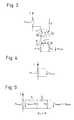
- a first combination of nullator N 1 and norator / N 1 with associated resistors R 1 and R 2 corresponding to the transistor amplifier from the prior art according to FIG. 5, a second nullator norator combination (broken line B 2) upstream shunt in the direction of the shunt resistor R. More precisely, a second nullator N L of the second nullator-norator combination B 2 lies in series with the first nullator N 1 , while the assigned second norator / N L is connected to ground via a resistor R 3 .
- the arrows pointing from the norator to the nullator symbolize the repercussions (modulations) of the relevant norator corresponding to an actual, non-linear behavior on the associated nullator.
- a further nullator N 3 is shown, which has the output of the first norator / N 1 (and therefore the output for the measurement voltage U mess ) on the input of the second norator / N L feeds back, with the operating current for the second (compensating) nullator-norator combination B 2 being set by means of resistor R 3 such that it corresponds to the operating current of the first nullator / norator combination and the coupling factor is determined by the resistance value R 3 .
- FIG. 2 illustrates a specific implementation in terms of circuitry of the symbolic network circuit diagram according to FIG. 1, the first nullator-norator combination N 1 , / N 1 being implemented by an npn / pnp transistor pair 10, 12, the second nullator-norator Combination B 2 is implemented by an npn transistor 14, and the third nullator N 3 is implemented as a further pnp transistor 16.
- transistors 10 to 16 which form a double current mirror in the circuit shown
- this further transistor 18 is connected in an otherwise known manner by resistors R 4 and R 5 .
- the additional amplifier stage with transistor 18 only serves to reverse a negative polarity of the amplified voltage signal at the collector of transistors 10 and 12.
- the transistor 16 connected as the operating current generator for the transistor 14 with the resistor k • R 2 achieves a feedback which, by means of an oppositely connected characteristic, compensates for a non-linearity of the transistor 10 with its own non-linear amplification, so that the result is an amplifier arrangement arises that has largely linear gain properties over a wide gain range and is therefore suitable for accurate current measurements.
- this arrangement is characterized by a comparatively simple circuit structure (is therefore particularly suitable for integration in an integrated circuit) and has a high maximum cutoff frequency, which is particularly suitable for use in connection with voltage converters in power electronics.
- this creates an arrangement that with a typical shunt resistance of about 1 to 500 mOhm, preferably 10 to 200 milliohm and a shunt voltage in the millivolt range, typically 10 to 50 millivolt, realized a gain factor of the order of 10.
- the amplifier circuit is up to three digits MHz range usable.
- FIG. 3 shows an alternative form of implementation of the exemplary embodiment 2, such that transistors 20 to 26 a corresponding (double) current mirror circuit realize, but with reversed polarity of the transistors used, so that a downstream Amplifier stage (using transistor 18 in Fig. 2) for polarity reversal can be omitted.
- the present invention is not limited to the exemplary embodiments shown limited. So it is particularly useful on, the embodiments shown, instead of with to realize discrete transistor components, also by implement appropriate integrated circuit environments, it being particularly preferred here that the respectively assigned Resistance through suitable dimensioning of the semiconductor elements itself or the corresponding endowed Realize areas and tracks. Alternatively, it is possible and encompassed by the present invention for principle explanation of the present invention used Network bipoles Norator and Nullator in the shown Way through other semiconductor devices, such as operational amplifiers or the like to implement.
Landscapes
- Physics & Mathematics (AREA)
- General Physics & Mathematics (AREA)
- Amplifiers (AREA)
- Measurement Of Current Or Voltage (AREA)
Applications Claiming Priority (2)
| Application Number | Priority Date | Filing Date | Title |
|---|---|---|---|
| DE10109833A DE10109833A1 (de) | 2001-03-01 | 2001-03-01 | Vorrichtung zur leistungsarmen Stromerfassung |
| DE10109833 | 2001-03-01 |
Publications (2)
| Publication Number | Publication Date |
|---|---|
| EP1237006A2 true EP1237006A2 (fr) | 2002-09-04 |
| EP1237006A3 EP1237006A3 (fr) | 2004-02-11 |
Family
ID=7675915
Family Applications (1)
| Application Number | Title | Priority Date | Filing Date |
|---|---|---|---|
| EP01130955A Withdrawn EP1237006A3 (fr) | 2001-03-01 | 2001-12-28 | Appareil de mesure de courant à faible perte |
Country Status (3)
| Country | Link |
|---|---|
| US (1) | US20020121893A1 (fr) |
| EP (1) | EP1237006A3 (fr) |
| DE (1) | DE10109833A1 (fr) |
Family Cites Families (2)
| Publication number | Priority date | Publication date | Assignee | Title |
|---|---|---|---|---|
| DE2503008A1 (de) * | 1974-01-29 | 1975-07-31 | Nat Res Dev | Variable impedanzen |
| US6028426A (en) * | 1997-08-19 | 2000-02-22 | Statpower Technologies Partnership | Temperature compensated current measurement device |
-
2001
- 2001-03-01 DE DE10109833A patent/DE10109833A1/de not_active Withdrawn
- 2001-12-28 EP EP01130955A patent/EP1237006A3/fr not_active Withdrawn
-
2002
- 2002-02-26 US US10/083,221 patent/US20020121893A1/en not_active Abandoned
Also Published As
| Publication number | Publication date |
|---|---|
| DE10109833A1 (de) | 2002-09-05 |
| US20020121893A1 (en) | 2002-09-05 |
| EP1237006A3 (fr) | 2004-02-11 |
Similar Documents
| Publication | Publication Date | Title |
|---|---|---|
| EP0744828B1 (fr) | Circuit amplificateur à transimpédance | |
| DE2811626A1 (de) | Filter fuer digital-analog-wandler | |
| EP0351639A2 (fr) | Circuit d'entrée pour amplificateur haute fréquence | |
| EP0726647B1 (fr) | Circuit amplificateur transimpédance | |
| DE4104980C2 (de) | Verstärkerstufe für niederohmige Wechselspannungs-Quellen | |
| DE102004022991B3 (de) | Abtast-Differenzverstärker und Abtast-Verstärker | |
| DE2646386A1 (de) | Transistorverstaerker | |
| DE102008025347B4 (de) | Elektronischer Verstärker | |
| EP1237006A2 (fr) | Appareil de mesure de courant à faible perte | |
| EP0429717B1 (fr) | Amplificateur de transconductance | |
| EP0133618A1 (fr) | Circuit oscillateur haute fréquence à quartz sous forme de circuit intégré monolithique | |
| DE69023741T2 (de) | Transistorverstärker mit veränderlichen Vorspannungsschaltungen. | |
| DE2156166B2 (de) | Dämpfungsfreier elektronischer Schalter | |
| DE2840822C3 (de) | Schaltungsanordnung zur Verstärkung von Videosignalen | |
| EP0893880B1 (fr) | Etage amplificateur à impédance d'entrée constante | |
| EP0607789B1 (fr) | Circuit pour générer un signal de sortie exponentielle dépendant d'un signal d'entrée | |
| EP0485853B1 (fr) | Etage de sortie pour amplificateur | |
| DE2637500C2 (de) | Leistungsverstärker zur Verstärkung elektrischer Spannungen | |
| DE10001530A1 (de) | Elektrische Schaltungsanordnung zur Umformung einer elektrischen Eingangsgröße in eine eingeprägte elektrische Ausgangsspannung | |
| DD222748A1 (de) | Optoelektronische empfangsanordnung | |
| DE1588255C (fr) | ||
| DE1762912C (de) | Schaltungsanordnung zur Wiedereinführung des Gleichspannungswertes in Fernsehsignale u.dgl. (Klemmschaltung) | |
| EP0217147A1 (fr) | Disposition de circuit pour alimenter en signaux un appareil de mesure à aimant rotatif | |
| DE1537701C (de) | Schaltungsanordnung zur galvanischen Kopplung von Verstärkerstufen | |
| DE4118151A1 (de) | Schaltungsanordnung mit einem transistor in kollektorschaltung |
Legal Events
| Date | Code | Title | Description |
|---|---|---|---|
| PUAI | Public reference made under article 153(3) epc to a published international application that has entered the european phase |
Free format text: ORIGINAL CODE: 0009012 |
|
| AK | Designated contracting states |
Kind code of ref document: A2 Designated state(s): AT BE CH CY DE DK ES FI FR GB GR IE IT LI LU MC NL PT SE TR |
|
| AX | Request for extension of the european patent |
Free format text: AL;LT;LV;MK;RO;SI |
|
| PUAL | Search report despatched |
Free format text: ORIGINAL CODE: 0009013 |
|
| AK | Designated contracting states |
Kind code of ref document: A3 Designated state(s): AT BE CH CY DE DK ES FI FR GB GR IE IT LI LU MC NL PT SE TR |
|
| AX | Request for extension of the european patent |
Extension state: AL LT LV MK RO SI |
|
| AKX | Designation fees paid | ||
| REG | Reference to a national code |
Ref country code: DE Ref legal event code: 8566 |
|
| STAA | Information on the status of an ep patent application or granted ep patent |
Free format text: STATUS: THE APPLICATION IS DEEMED TO BE WITHDRAWN |
|
| 18D | Application deemed to be withdrawn |
Effective date: 20040812 |