EP1237006A2 - Low loss current measuring device - Google Patents
Low loss current measuring device Download PDFInfo
- Publication number
- EP1237006A2 EP1237006A2 EP01130955A EP01130955A EP1237006A2 EP 1237006 A2 EP1237006 A2 EP 1237006A2 EP 01130955 A EP01130955 A EP 01130955A EP 01130955 A EP01130955 A EP 01130955A EP 1237006 A2 EP1237006 A2 EP 1237006A2
- Authority
- EP
- European Patent Office
- Prior art keywords
- nullator
- norator
- shunt
- combination
- norator combination
- Prior art date
- Legal status (The legal status is an assumption and is not a legal conclusion. Google has not performed a legal analysis and makes no representation as to the accuracy of the status listed.)
- Withdrawn
Links
Images

Classifications
-
- G—PHYSICS
- G01—MEASURING; TESTING
- G01R—MEASURING ELECTRIC VARIABLES; MEASURING MAGNETIC VARIABLES
- G01R19/00—Arrangements for measuring currents or voltages or for indicating presence or sign thereof
- G01R19/0092—Measuring current only
Definitions
- the present invention relates to a device for Low power current detection using a shunt voltage generating shunt resistance.
- Such a current measurement for generating a measurement voltage U mess across a shunt resistor R shunt is known from the prior art as a basic way of measuring current.
- a possible procedure known from the prior art to reduce the power loss would be by means of Current transformer, such as a transformer.
- a transformer is suitable for current detection due to its magnetic properties (or the necessity of such a current transformer, periodically not demagnetize itself).
- a transistor can be described as a nullator-norator equivalent circuit diagram in such a way that the base-emitter transition is described by the nullator and the collector-emitter transition by the norator;
- the nullator and norator are connected accordingly at the emitter, so that ideally the base emitter voltage is zero and the base current is zero, and the collector-emitter voltage and the collector current are dependent on the external wiring.
- the resistance R 1 corresponds to the emitter resistance and R 2 corresponds to the collector resistance, the gain factor -x for the measurement voltage U mess being formed as the quotient of R 2 and R 1 .
- the gain is negative (ie with polarity reversal), so that typically the arrangement according to FIG. 5 has a further transistor stage (as basically the same nullator-norator combination) is connected with an assumed gain -y and the total gain x • y thus becomes positive.
- the object of the present invention is therefore in generic Measuring arrangements for low-power current detection by means of shunt resistance the linearity of a downstream Improve amplifier network, the Power loss above the shunt resistance (and therefore the deterioration in efficiency caused by current measurement) should remain minimized.
- the first is advantageously provided Nullator-Norator combination a second Nullator-Norator combination, preferably as a transistor or Transistor pair realized, so that by the second nullator-norator combination to compensate for one non-linear gain behavior of the first nullator-norator combination can be done.
- This is achieved through a feedback, the feedback signal for the second Nullator-Norator combination at the exit of the first combination is produced.
- the respective are in a particularly particularly meaningful manner Nullator-Norator combinations as transistors or Transistor pairs implemented, the current through the second nullator-norator combination (as a transistor) with Using another nullator (same transistor pair) is set so that in the series connection from the first Nullator (the first combination) and second nullator (off the second combination) the desired linearization effect arises.
- the degree of feedback (what is important is a swing or oscillation of the arrangement is suppressed) set by the respective emitter resistors. While for this on the one hand resistance components or discrete Resistors can be used, it offers also within the scope of the present invention, such resistance values by appropriate dimensioning of the used Adjust semiconductor itself; this approach is in particular for realizing the present invention Amplifier topology as an integrated circuit suitable.
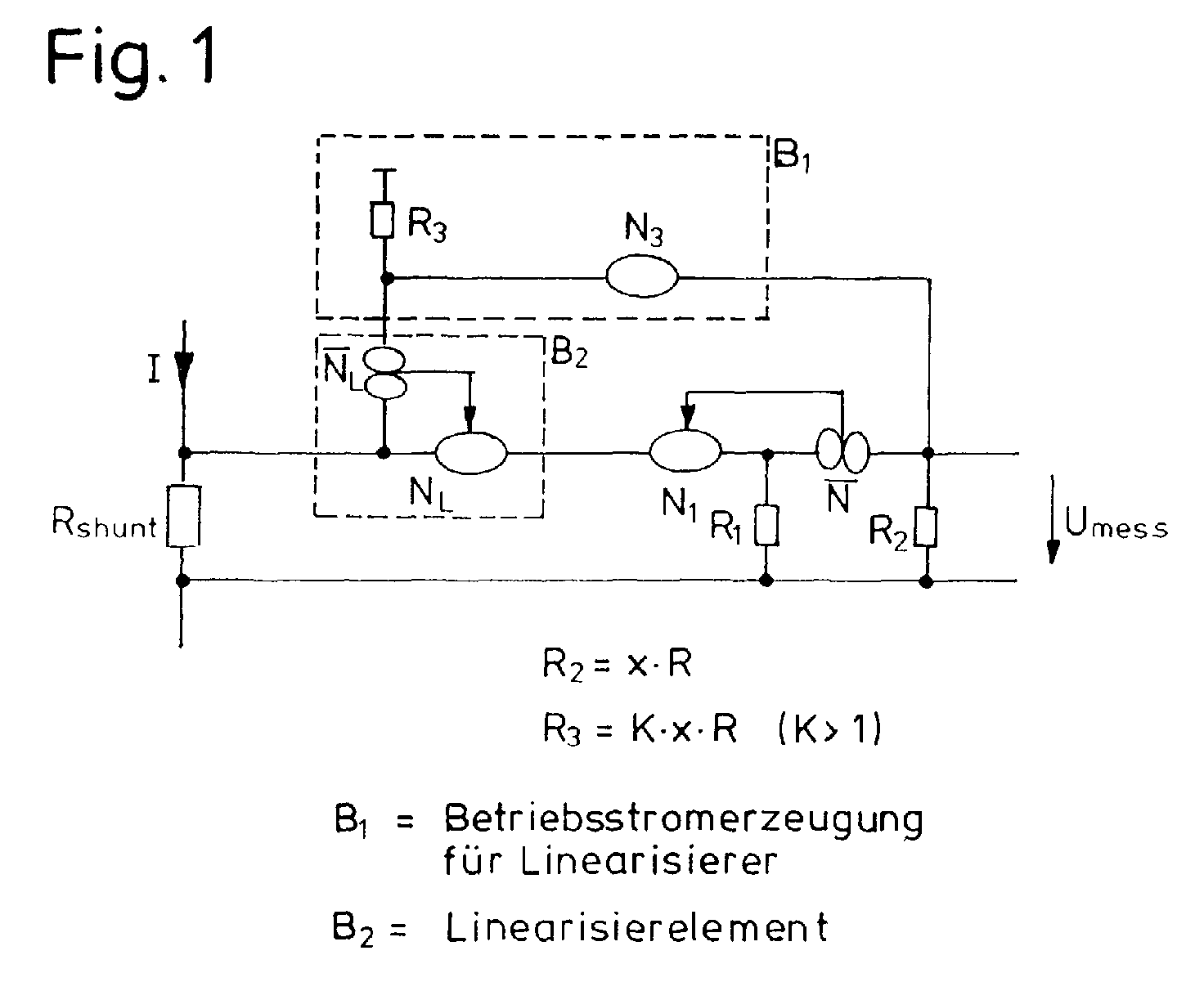
- a first combination of nullator N 1 and norator / N 1 with associated resistors R 1 and R 2 corresponding to the transistor amplifier from the prior art according to FIG. 5, a second nullator norator combination (broken line B 2) upstream shunt in the direction of the shunt resistor R. More precisely, a second nullator N L of the second nullator-norator combination B 2 lies in series with the first nullator N 1 , while the assigned second norator / N L is connected to ground via a resistor R 3 .
- the arrows pointing from the norator to the nullator symbolize the repercussions (modulations) of the relevant norator corresponding to an actual, non-linear behavior on the associated nullator.
- a further nullator N 3 is shown, which has the output of the first norator / N 1 (and therefore the output for the measurement voltage U mess ) on the input of the second norator / N L feeds back, with the operating current for the second (compensating) nullator-norator combination B 2 being set by means of resistor R 3 such that it corresponds to the operating current of the first nullator / norator combination and the coupling factor is determined by the resistance value R 3 .
- FIG. 2 illustrates a specific implementation in terms of circuitry of the symbolic network circuit diagram according to FIG. 1, the first nullator-norator combination N 1 , / N 1 being implemented by an npn / pnp transistor pair 10, 12, the second nullator-norator Combination B 2 is implemented by an npn transistor 14, and the third nullator N 3 is implemented as a further pnp transistor 16.
- transistors 10 to 16 which form a double current mirror in the circuit shown
- this further transistor 18 is connected in an otherwise known manner by resistors R 4 and R 5 .
- the additional amplifier stage with transistor 18 only serves to reverse a negative polarity of the amplified voltage signal at the collector of transistors 10 and 12.
- the transistor 16 connected as the operating current generator for the transistor 14 with the resistor k • R 2 achieves a feedback which, by means of an oppositely connected characteristic, compensates for a non-linearity of the transistor 10 with its own non-linear amplification, so that the result is an amplifier arrangement arises that has largely linear gain properties over a wide gain range and is therefore suitable for accurate current measurements.
- this arrangement is characterized by a comparatively simple circuit structure (is therefore particularly suitable for integration in an integrated circuit) and has a high maximum cutoff frequency, which is particularly suitable for use in connection with voltage converters in power electronics.
- this creates an arrangement that with a typical shunt resistance of about 1 to 500 mOhm, preferably 10 to 200 milliohm and a shunt voltage in the millivolt range, typically 10 to 50 millivolt, realized a gain factor of the order of 10.
- the amplifier circuit is up to three digits MHz range usable.
- FIG. 3 shows an alternative form of implementation of the exemplary embodiment 2, such that transistors 20 to 26 a corresponding (double) current mirror circuit realize, but with reversed polarity of the transistors used, so that a downstream Amplifier stage (using transistor 18 in Fig. 2) for polarity reversal can be omitted.
- the present invention is not limited to the exemplary embodiments shown limited. So it is particularly useful on, the embodiments shown, instead of with to realize discrete transistor components, also by implement appropriate integrated circuit environments, it being particularly preferred here that the respectively assigned Resistance through suitable dimensioning of the semiconductor elements itself or the corresponding endowed Realize areas and tracks. Alternatively, it is possible and encompassed by the present invention for principle explanation of the present invention used Network bipoles Norator and Nullator in the shown Way through other semiconductor devices, such as operational amplifiers or the like to implement.
Landscapes
- Physics & Mathematics (AREA)
- General Physics & Mathematics (AREA)
- Amplifiers (AREA)
- Measurement Of Current Or Voltage (AREA)
Abstract
Die Erfindung betrifft eine Vorrichtung zur leistungsarmen
Stromerfassung mittels eines eine Shuntspannung erzeugenden
Shuntwiderstands (Rshunt), mit einem zum Verstärken der
Shuntspannung in eine Messspannung ausgebildeten Verstärkernetzwerk,
das eine erste, als Verstärker beschaltete
Nullator-Norator-Kombination (N1, /N1) aufweist, wobei der
ersten Nullator-Norator-Kombination eine zweite Nullator-Norator-Kombination
(B2) in Richtung auf den Shuntwiderstand
so in Reihe vorgeschaltet ist, dass der erste Nullator
und der zweite Nullator in einer Rückkopplung betrieben
werden und eine Nichtlinearität des ersten Nullators durch
ein entgegengesetztes Verhalten des zweiten Nullators kompensiert
werden kann, wobei ein Rückkoppelsignal für die
zweite Nullator-Norator-Kombination am Ausgang der ersten
Nullator-Norator-Kombination abgegriffen wird.
Description
Die vorliegende Erfindung betrifft eine Vorrichtung zur leistungsarmen Stromerfassung mittels eines eine Shuntspannung erzeugenden Shuntwiderstandes.The present invention relates to a device for Low power current detection using a shunt voltage generating shunt resistance.
Eine derartige Strommessung zum Erzeugen einer Messspannung Umess über einem Shuntwiderstand Rshunt, wie schematisch in Fig. 4 gezeigt, ist aus dem Stand der Technik als prinzipieller Weg zur Strommessung bekannt.Such a current measurement for generating a measurement voltage U mess across a shunt resistor R shunt , as shown schematically in FIG. 4, is known from the prior art as a basic way of measuring current.
Insbesondere in der Leistungselektronik, etwa bei Spannungswandlern, weisen gängige integrierte Schaltungen zur Ansteuerung entsprechender Leistungshalbleiter einen Eingang zur Regelung eines üblicherweise induktiven Stromes auf, wobei der erforderliche Spannungspegel, im Bereich von etwa 1 Volt, vergleichsweise hoch ist, um für einen günstigen Rausch-Spannungs-Abstand zu sorgen. Eine Stromerfassung erfordert hier (je nach Leistung) relativ große Widerstandswerte für einen Shuntwiderstand, mit damit verbundenen relativ hohen Verlusten und negativen Auswirkungen auf den Wirkungsgrad.Especially in power electronics, such as voltage converters, assign common integrated circuits Control of corresponding power semiconductors an input to regulate a usually inductive current with the required voltage level, in the range of about 1 volt, which is comparatively high, for a cheap one To provide noise-voltage gap. A current measurement requires relatively large resistance values (depending on the performance) for a shunt resistor, with associated relatively high losses and negative impacts the efficiency.
Eine aus dem Stand der Technik bekannte, mögliche Vorgehensweise zur Senkung der Verlustleistung wäre mittels eines Stromwandlers, etwa eines Transformators. Für eine dauernde Stromerfassung eignet sich jedoch ein Transformator aufgrund seiner magnetischen Eigenschaften (bzw. der Notwendigkeit eines solchen Stromwandlers, sich periodisch selbst zu entmagnetisieren) nicht.A possible procedure known from the prior art to reduce the power loss would be by means of Current transformer, such as a transformer. For a permanent However, a transformer is suitable for current detection due to its magnetic properties (or the necessity of such a current transformer, periodically not demagnetize itself).
Entsprechend könnte es sich daher anbieten, einen (zur Verminderung der Verlustleistung) kleinen Shuntwiderstand zu wählen und das entsprechend kleine Messsignal Umess durch einen geeigneten Verstärker zu verstärken, um dann eine geeignete Stromerfassung mittels einer nachgeschalteten Schaltungseinheit durchführen zu können. Accordingly, it could be appropriate to choose a small shunt resistance (to reduce the power loss) and to amplify the correspondingly small measurement signal U mess by a suitable amplifier, in order then to be able to carry out a suitable current detection by means of a downstream circuit unit.
Gängige, halbleiterbasierte Verstärkertopologien weisen allerdings den Nachteil auf, dass diese, insbesondere wenn sie mehrstufig realisiert sind, aufwendig im Aufbau sind, oftmals über den Verstärkungsbereich eine nicht lineare Verstärkungscharakteristik aufweisen und zudem nur in einem begrenzten Frequenzbereich betreibbar sind, d.h. in ihrer nutzbaren Frequenzbandbreite limitiert sind.Common, semiconductor-based amplifier topologies, however, show the disadvantage that this, especially if they are implemented in several stages, are complex to set up, often a non-linear one over the gain range Have amplification characteristics and also only in one limited frequency range can be operated, i.e. in your usable frequency bandwidth are limited.
Insbesondere das Problem der Nichtlinearität eines gattungsbildenden, üblichen einstufigen Transistorverstärkers soll anhand des Prinzipschaltbildes der Figur 5 erläutert werden, wobei ein dem Shuntwiderstand Rshunt nachgeschalteter Verstärkertransistor mit Hilfe der aus der Netzwerktheorie bekannten Zweipole "Nullator" N1 sowie "Norator"/N1, wie in der Fig. 5 mit Widerständen R1, R2 beschaltet, beschrieben werden soll. Genauer gesagt läßt sich ein Transistor als Nullator-Norator-Ersatzschaltbild derart beschreiben, dass der Basis-Emitterübergang durch den Nullator, und der Kollektor-Emitterübergang durch den Norator beschrieben werden; Nullator und Norator sind entsprechend am Emitter verbunden, so dass idealisiert die BasisEmitterspannung gleich Null sowie der Basisstrom gleich Null sind, und die Kollektor-Emitterspannung sowie der Kollektorstrom von der äußeren Beschaltung abhängig sind. Im Verstärker-Ersatzschaltbild der Fig. 5 entspricht dabei der Widerstand R1 dem Emitterwiderstand, und R2 dem Kollektorwiderstand, wobei sich der Verstärkungsfaktor -x für die Messspannung Umess als Quotient von R2 und R1 bildet. Bei dem in Fig. 5 gezeigten, prinzipiellen Ersatzschaltbild aus dem Stand der Technik ist dabei die Verstärkung negativ (d.h. mit Umkehrung der Polarität), so dass typischerweise der Anordnung nach Fig. 5 eine weitere Transistorstufe (als prinzipiell dieselbe Nullator-Norator-Kombination) mit einer angenommenen Verstärkung -y nachgeschaltet ist und die Gesamtverstärkung x • y damit positiv wird. In particular, the problem of the non-linearity of a generic, conventional single-stage transistor amplifier is to be explained on the basis of the basic circuit diagram of FIG. 5, an amplifier transistor connected downstream of the shunt resistor R shunt using the two-pole "nullator" N1 and "norator" / N1 known from network theory, as in 5 with resistors R 1 , R 2 is to be described. More precisely, a transistor can be described as a nullator-norator equivalent circuit diagram in such a way that the base-emitter transition is described by the nullator and the collector-emitter transition by the norator; The nullator and norator are connected accordingly at the emitter, so that ideally the base emitter voltage is zero and the base current is zero, and the collector-emitter voltage and the collector current are dependent on the external wiring. In the amplifier equivalent circuit diagram of FIG. 5, the resistance R 1 corresponds to the emitter resistance and R 2 corresponds to the collector resistance, the gain factor -x for the measurement voltage U mess being formed as the quotient of R 2 and R 1 . In the case of the basic equivalent circuit diagram from the prior art shown in FIG. 5, the gain is negative (ie with polarity reversal), so that typically the arrangement according to FIG. 5 has a further transistor stage (as basically the same nullator-norator combination) is connected with an assumed gain -y and the total gain x • y thus becomes positive.
Bei der Anordnung der Fig. 5 handelt es sich, wie gesagt, um einen ansonsten bekannten einstufigen Transistorverstärker, wobei die verwendete Form der Beschreibung mit den aus der Netzwerktheorie bekannten, idealisierten Netzwerkelementen Norator und Nullator noch auf ein prinzipbedingtes Problem hinweist, nämlich eine tatsächliche Nichtlinearität des Nullators N1, wenn dieser mit konkreten Bauelementen, z. B. einem Transistor, realisiert ist, mit einer entsprechend nachteiligen Wirkung auf die Genauigkeit der Messanordnung über den Gesamtbereich. Diese tatsächliche Nichtlinearität ist das Ergebnis einer Beeinflussung (Modulation) des Nullators durch den zugehörigen Norator/N1 und führt zu der nichtlinearen Verstärkungscharakteristik des Systems und mithin dessen schlechter Eignung für eine hochpräzise Stromerfassung.5, as mentioned, is an otherwise known single-stage transistor amplifier, the form of the description used with the idealized network elements known from network theory Norator and Nullator still pointing to a principle-related problem, namely an actual non-linearity the nullator N 1 , if this with concrete components, for. B. a transistor is realized, with a correspondingly adverse effect on the accuracy of the measuring arrangement over the entire range. This actual non-linearity is the result of an influencing (modulation) of the nullator by the associated norator / N 1 and leads to the non-linear amplification characteristic of the system and therefore its poor suitability for high-precision current detection.
Aufgabe der vorliegenden Erfindung ist es daher, bei gattungsbildenden Messanordnungen zur leistungsarmen Stromerfassung mittels Shuntwiderstand die Linearität eines nachgeschalteten Verstärkernetzwerkes zu verbessern, wobei die Verlustleistung über dem Shuntwiderstand (und mithin die durch die Strommessung bewirkte Verschlechterung des Wirkungsgrades) minimiert bleiben soll.The object of the present invention is therefore in generic Measuring arrangements for low-power current detection by means of shunt resistance the linearity of a downstream Improve amplifier network, the Power loss above the shunt resistance (and therefore the deterioration in efficiency caused by current measurement) should remain minimized.
Die Aufgabe wird durch die Vorrichtung mit den Merkmalen
des Patentanspruches 1 gelöst, wobei, wie im Patentanspruch
9 beansprucht, sich die vorliegende Erfindung insbesondere
zur Verwendung mit Spannungswandlern in der Leistungselektronik,
und dort weiter bevorzugt für DC-DC-Wandler, eignet.
Vorteilhafte Weiterbildungen der Erfindung sind in den
Unteransprüchen beschrieben.The task is accomplished by the device with the features
of
So ist erfindungsgemäß und vorteilhaft vorgesehen, der ersten Nullator-Norator-Kombination eine zweite Nullator-Norator-Kombination, bevorzugt jeweils als Transistor bzw. Transistorpaar realisiert, so vorzuschalten, dass durch die zweite Nullator-Norator-Kombination eine Kompensation eines nichtlinearen Verstärkungsverhaltens der ersten Nullator-Norator-Kombination erfolgen kann. Erreicht wird dies durch eine Rückkopplung, wobei das Rückkoppelsignal für die zweite Nullator-Norator-Kombination am Ausgang der ersten Kombination erzeugt wird.Thus, according to the invention, the first is advantageously provided Nullator-Norator combination a second Nullator-Norator combination, preferably as a transistor or Transistor pair realized, so that by the second nullator-norator combination to compensate for one non-linear gain behavior of the first nullator-norator combination can be done. This is achieved through a feedback, the feedback signal for the second Nullator-Norator combination at the exit of the first combination is produced.
In praktisch besonders bedeutsamer Weise werden die jeweiligen Nullator-Norator-Kombinationen als Transistoren bzw. Transistorpaare implementiert, wobei der Strom durch die zweite Nullator-Norator-Kombination (als Transistor) mit Hilfe eines weiteren Nullators (desselben Transistorpaares) so eingestellt wird, dass in der Reihenschaltung aus erstem Nullator (der ersten Kombination) und zweitem Nullator (aus der zweiten Kombination) der gewünschte Linearisierungseffekt entsteht.The respective are in a particularly particularly meaningful manner Nullator-Norator combinations as transistors or Transistor pairs implemented, the current through the second nullator-norator combination (as a transistor) with Using another nullator (same transistor pair) is set so that in the series connection from the first Nullator (the first combination) and second nullator (off the second combination) the desired linearization effect arises.
Der Grad der Rückkopplung (wichtig ist, dass ein Schwingen bzw. Aufschwingen der Anordnung unterdrückt wird) wird dabei durch die jeweiligen Emitterwiderstände eingestellt. Während hierfür einerseits Widerstandsbauelemente bzw. diskrete Widerstände verwendet werden können, bietet es sich auch im Rahmen der vorliegenden Erfindung an, derartige Widerstandswerte durch entsprechende Dimensionierung der verwendeten Halbleiter selbst einzustellen; dieser Ansatz ist insbesondere für eine Realisierung der vorliegenden, erfindungsgemäßen Verstärkertopologie als integrierte Schaltung geeignet.The degree of feedback (what is important is a swing or oscillation of the arrangement is suppressed) set by the respective emitter resistors. While for this on the one hand resistance components or discrete Resistors can be used, it offers also within the scope of the present invention, such resistance values by appropriate dimensioning of the used Adjust semiconductor itself; this approach is in particular for realizing the present invention Amplifier topology as an integrated circuit suitable.
Im Ergebnis läßt sich so eine äußerst (verlust-) leistungsarme Stromerfassung realisieren, da, zum Erzeugen einer Shuntspannung im Millivolt-Bereich, lediglich ein Shuntwiderstand im Milliohm-Bereich notwendig ist. Gleichzeitig ermöglicht es das vorliegende Erfindungsprinzip, eine sehr hohe maximale Grenzfrequenz zu realisieren, so dass die erfindungsgemäße Stromerfassung nicht nur über den Verstärkungsbereich hochgradig linear ist, sondern zudem eine hohe nutzbare Bandbreite der Betriebsfrequenz aufweist. The result is an extremely low (loss) performance Realize current detection, there, to generate a Shunt voltage in the millivolt range, just a shunt resistance in the milliohm range is necessary. simultaneously allows the present principle of the invention, a very Realize high maximum cutoff frequency, so that the invention Current acquisition not only over the gain range is highly linear, but also high Usable bandwidth of the operating frequency.
Weitere Vorteile, Merkmale und Einzelheiten der Erfindung ergeben sich aus der nachfolgenden Beschreibung bevorzugter Ausführungsbeispiele sowie anhand der Zeichnungen; diese zeigen in
- Fig. 1:
- ein erstes, schematisches Schaltbild einer erfindungsgemäßen Vorrichtung zur leistungsarmen Stromerfassung gemäß einer ersten, bevorzugten Ausführungsform der Erfindung;
- Fig. 2:
- eine konkrete schaltungstechnische Realisierung der Ausführungsform gemäß Fig. 1;
- Fig. 3:
- eine zweite, alternative Ausführungsform der vorliegenden Erfindung;
- Fig. 4:
- ein generelles Prinzip zur Strommessung mittels Shuntwiderstand aus dem Stand der Technik und
- Fig. 5:
- ein Prinzipschaltbild einer Strommessung mittels Shuntwiderstand sowie nachgeschaltetem, einstufigem Transistorverstärker, welcher als Nullator-Norator-Kombination dargestellt ist.
- Fig. 1:
- a first schematic circuit diagram of a device according to the invention for low power current detection according to a first preferred embodiment of the invention;
- Fig. 2:
- a concrete circuit implementation of the embodiment according to FIG. 1;
- Fig. 3:
- a second, alternative embodiment of the present invention;
- Fig. 4:
- a general principle for current measurement using shunt resistance from the prior art and
- Fig. 5:
- a schematic diagram of a current measurement using a shunt resistor and a downstream, single-stage transistor amplifier, which is shown as a nullator-norator combination.
Unter Bezug auf Fig. 1 wird deutlich, dass eine erste Kombination aus Nullator N1 und Norator/N1 mit zugehörigen Widerständen R1 bzw. R2, entsprechend dem Transistorverstärker aus dem Stand der Technik gemäß Fig. 5, eine zweite Nullator-Norator-Kombination (gestrichelte Linie B2) in Richtung auf den Shuntwiderstand Rshunt vorgeschaltet aufweist. Genauer gesagt liegt ein zweiter Nullator NL der zweiten Nullator-Norator-Kombination B2 in Reihe mit dem ersten Nullator N1, während der zugeordnete zweite Norator/NL über einen Widerstand R3 mit Masse verbunden ist. In der Fig. 1 symbolisieren die jeweils vom Norator auf den Nullator weisenden Pfeile die einem tatsächlichen, nichtlinearen Verhalten entsprechenden Rückwirkungen (Modulationen) des betreffenden Norators auf den zugehörigen Nullator.With reference to FIG. 1 it is clear that a first combination of nullator N 1 and norator / N 1 with associated resistors R 1 and R 2 , corresponding to the transistor amplifier from the prior art according to FIG. 5, a second nullator norator combination (broken line B 2) upstream shunt in the direction of the shunt resistor R. More precisely, a second nullator N L of the second nullator-norator combination B 2 lies in series with the first nullator N 1 , while the assigned second norator / N L is connected to ground via a resistor R 3 . In FIG. 1, the arrows pointing from the norator to the nullator symbolize the repercussions (modulations) of the relevant norator corresponding to an actual, non-linear behavior on the associated nullator.
Zusätzlich ist in Fig. 1, symbolisiert mit der gestrichelten Linie B1, ein weiterer Nullator N3 gezeigt, welcher den Ausgang des ersten Norators/N1 (und mithin den Ausgang für die Messspannung Umess) auf den Eingang des zweiten Norators/NL rückkoppelt, wobei mittels Widerstand R3 der Betriebsstrom für die zweite (kompensierende) Nullator-Norator-Kombination B2 so eingestellt wird, dass er dem Betriebsstrom der ersten Nullator/Norator-Kombination entspricht und der Kopplungsfaktor durch den Widerstandswert R3 bestimmt wird.In addition, in FIG. 1, symbolized by the dashed line B 1 , a further nullator N 3 is shown, which has the output of the first norator / N 1 (and therefore the output for the measurement voltage U mess ) on the input of the second norator / N L feeds back, with the operating current for the second (compensating) nullator-norator combination B 2 being set by means of resistor R 3 such that it corresponds to the operating current of the first nullator / norator combination and the coupling factor is determined by the resistance value R 3 .
Genauer gesagt bestimmt sich die Verstärkung der in Fig. 1
symbolisch gezeigten Anordnung wiederum durch den Faktor x
als Quotient von R2 und R1, und auch ein Verstärkungsfaktor
bzw. Kopplungsfaktor k der zweiten Nullator-Norator-Kombination
B2 bestimmt sich analog als Quotient aus R3 und R2,
so dass gelten muss:
Die Fig. 2 verdeutlicht eine konkrete schaltungstechnische
Umsetzung des symbolischen Netzwerkschaltbildes gemäß Fig.
1, wobei die erste Nullator-Norator-Kombination N1, /N1
durch ein npn/pnp-Transistorpaar 10, 12 realisiert ist, die
zweite Nullator-Norator-Kombination B2 durch einen npn-Transistor
14 realisiert ist, und der dritte Nullator N3
als weiterer pnp-Transistor 16 realisiert ist. Entsprechend
findet eine Einstellung der Rückkopplung durch geeignete
Bemessung des Faktors k für den Emitterwiderstand R3 =
k • R2 für den Transistor 16, relativ zum Emitterwiderstand
R2 für den Transistor 12 statt, und der Verstärkungsfaktor
für die Schaltanordnung am Kollektorausgang der Transistoren
12 bzw. 14 bestimmt sich entsprechend durch den Quotienten
aus Emitterwiderstand R2 und Emitterwiderstand R1 für
den Transistor 10.FIG. 2 illustrates a specific implementation in terms of circuitry of the symbolic network circuit diagram according to FIG. 1, the first nullator-norator combination N 1 , / N 1 being implemented by an npn /
Wie sich aus der Fig. 2 zudem ergibt, ist der Anordnung aus
den Transistoren 10 bis 16 (die in der gezeigten Verschaltung
einen doppelten Stromspiegel ausbilden) eine weitere
Verstärkerstufe mittels Transistor 18 nachgeschaltet, an
welchem kollektorseitig dann die eigentliche Messspannung
Umess abgegriffen wird, wobei dieser weitere Transistor 18
in ansonsten bekannter Weise durch Widerstände R4 bzw. R5
beschaltet ist. Wie vorstehend bereits erläutert, dient die
zusätzliche Verstärkerstufe mit Transistor 18 jedoch lediglich
dazu, eine negative Polarität des verstärkten Spannungssignals
am Kollektor der Transistoren 10 bzw. 12 wiederum
umzukehren.As can also be seen from FIG. 2, the arrangement of
Im Betrieb wird durch den als Betriebsstromerzeuger für den
Transistor 14 mit dem Widerstand k • R2 beschalteten Transistor
16 eine Rückkopplung erreicht, die, durch entgegengesetzt
geschaltete Charakteristik, mit der eigenen nichtlinearen
Verstärkung eine Nichtlinearität des Transistors
10 kompensiert, so dass im Ergebnis eine Verstärkeranordnung
entsteht, die über einen weiten Verstärkungsbereich
weitgehend lineare Verstärkungseigenschaften aufweist
und somit für genaue Strommessungen geeignet ist.
Gleichzeitig zeichnet sich diese Anordnung durch einen vergleichsweise
einfachen Schaltungsaufbau aus (eignet sich
damit insbesondere auch für eine Integration in einem integrierten
Schaltkreis) und weist eine hohe maximale Grenzfrequenz
auf, die sich insbesondere auch für den Einsatz im
Zusammenhang mit Spannungswandlern in der Leistungselektronik
geeignet macht. In operation, the
In der praktischen Realisierung entsteht so eine Anordnung, die bei einem typischen Shuntwiderstand von etwa 1 bis 500 mOhm, bevorzugt 10 bis 200 Milliohm und einer Shuntspannung im Millivoltbereich, typischerweise 10 bis 50 Millivolt, einen Verstärkungsfaktor der Größenordnung von 10 realisiert. Die Verstärkerschaltung ist bis zum dreistelligen MHz-Bereich brauchbar.In practical implementation, this creates an arrangement that with a typical shunt resistance of about 1 to 500 mOhm, preferably 10 to 200 milliohm and a shunt voltage in the millivolt range, typically 10 to 50 millivolt, realized a gain factor of the order of 10. The amplifier circuit is up to three digits MHz range usable.
Fig. 3 zeigt eine alternative Realisierungsform des Ausführungsbeispiels
gemäß Fig. 2, dergestalt, dass Transistoren
20 bis 26 eine entsprechende (doppelte) Stromspiegelschaltung
realisieren, jedoch jeweils mit umgekehrter Polarität
der verwendeten Transistoren, so dass eine nachgeschaltete
Verstärkerstufe (mittels Transistor 18 in Fig. 2) zur Polaritätsumkehr
entfallen kann.3 shows an alternative form of implementation of the exemplary embodiment
2, such that
Die vorliegende Erfindung ist nicht auf die gezeigten Ausführungsbeispiele beschränkt. So bietet es sich insbesondere an, die gezeigten Ausführungsbeispiele, anstelle mit diskreten Transistorbauelementen zu realisieren, auch durch entsprechende integrierte Schaltungsumgebungen zu realisieren, wobei es hier besonders bevorzugt ist, die jeweils zugeordneten Widerstände durch geeignete Bemessung der Halbleiterelemente selbst bzw. der entsprechenden dotierten Flächen und Bahnen umzusetzen. Alternativ ist es möglich und von der vorliegenden Erfindung mitumfasst, die zur prinzipiellen Erläuterung der vorliegenden Erfindung verwendeten Netzwerk-Zweipole Norator und Nullator in der gezeigten Weise durch andere Halbleiterbauelemente, etwa Operationsverstärker od.dgl., zu implementieren.The present invention is not limited to the exemplary embodiments shown limited. So it is particularly useful on, the embodiments shown, instead of with to realize discrete transistor components, also by implement appropriate integrated circuit environments, it being particularly preferred here that the respectively assigned Resistance through suitable dimensioning of the semiconductor elements itself or the corresponding endowed Realize areas and tracks. Alternatively, it is possible and encompassed by the present invention for principle explanation of the present invention used Network bipoles Norator and Nullator in the shown Way through other semiconductor devices, such as operational amplifiers or the like to implement.
Claims (9)
einem zum Verstärken der Shuntspannung in eine Messspannung ausgebildeten Verstärkernetzwerk, das eine erste, als Verstärker beschaltete Nullator-Norator-Kombination (N1, /N1) aufweist,
dadurch gekennzeichnet, dass
der ersten Nullator-Norator-Kombination eine zweite Nullator-Norator-Kombination (B2) in Richtung auf den Shuntwiderstand so in Reihe vorgeschaltet ist, dass der erste Nullator und der zweite Nullator in einer Rückkopplung betrieben werden und eine Nichtlinearität des ersten Nullators durch ein entgegengesetztes Verhalten des zweiten Nullators kompensiert werden kann,
wobei ein Rückkoppelsignal für die zweite Nullator-Norator-Kombination am Ausgang der ersten Nullator-Norator-Kombination abgegriffen wird.Device for low-power current detection by means of a shunt resistor (R shunt ) generating a shunt voltage
an amplifier network designed to amplify the shunt voltage into a measurement voltage and which has a first nullator-norator combination (N 1 , / N 1 ) connected as an amplifier,
characterized in that
The first nullator-norator combination is preceded by a second nullator-norator combination (B 2 ) in series in the direction of the shunt resistance in such a way that the first nullator and the second nullator are operated in a feedback and a non-linearity of the first nullator opposite behavior of the second nullator can be compensated,
wherein a feedback signal for the second nullator-norator combination is tapped at the output of the first nullator-norator combination.
Applications Claiming Priority (2)
| Application Number | Priority Date | Filing Date | Title |
|---|---|---|---|
| DE10109833A DE10109833A1 (en) | 2001-03-01 | 2001-03-01 | Device for low-power current detection |
| DE10109833 | 2001-03-01 |
Publications (2)
| Publication Number | Publication Date |
|---|---|
| EP1237006A2 true EP1237006A2 (en) | 2002-09-04 |
| EP1237006A3 EP1237006A3 (en) | 2004-02-11 |
Family
ID=7675915
Family Applications (1)
| Application Number | Title | Priority Date | Filing Date |
|---|---|---|---|
| EP01130955A Withdrawn EP1237006A3 (en) | 2001-03-01 | 2001-12-28 | Low loss current measuring device |
Country Status (3)
| Country | Link |
|---|---|
| US (1) | US20020121893A1 (en) |
| EP (1) | EP1237006A3 (en) |
| DE (1) | DE10109833A1 (en) |
Family Cites Families (2)
| Publication number | Priority date | Publication date | Assignee | Title |
|---|---|---|---|---|
| DE2503008A1 (en) * | 1974-01-29 | 1975-07-31 | Nat Res Dev | VARIABLE IMPEDANCES |
| US6028426A (en) * | 1997-08-19 | 2000-02-22 | Statpower Technologies Partnership | Temperature compensated current measurement device |
-
2001
- 2001-03-01 DE DE10109833A patent/DE10109833A1/en not_active Withdrawn
- 2001-12-28 EP EP01130955A patent/EP1237006A3/en not_active Withdrawn
-
2002
- 2002-02-26 US US10/083,221 patent/US20020121893A1/en not_active Abandoned
Also Published As
| Publication number | Publication date |
|---|---|
| DE10109833A1 (en) | 2002-09-05 |
| US20020121893A1 (en) | 2002-09-05 |
| EP1237006A3 (en) | 2004-02-11 |
Similar Documents
| Publication | Publication Date | Title |
|---|---|---|
| EP0744828B1 (en) | Transimpedance amplifier circuit | |
| DE2811626A1 (en) | FILTER FOR DIGITAL-ANALOG CONVERTER | |
| EP0351639A2 (en) | Input circuit for a high-frequency amplifier | |
| EP0726647B1 (en) | Transimpedance amplifier circuit | |
| DE4104980C2 (en) | Amplifier stage for low-impedance AC sources | |
| DE102004022991B3 (en) | Sample differential amplifier and sample amplifier | |
| DE2646386A1 (en) | Isolation amplifier for video signal switching network - has complementary push-pull output transistors driven by complementary input transistors | |
| DE102008025347B4 (en) | Electronic amplifier | |
| EP1237006A2 (en) | Low loss current measuring device | |
| EP0429717B1 (en) | Transconductance amplifier | |
| EP0133618A1 (en) | Monolithic integrated transistor high-frequency quartz oscillator circuit | |
| DE69023741T2 (en) | Transistor amplifier with variable bias circuits. | |
| DE2156166B2 (en) | Attenuation-free electronic switch | |
| DE2840822C3 (en) | Circuit arrangement for amplifying video signals | |
| EP0893880B1 (en) | Amplifier stage with constant input impedance | |
| EP0607789B1 (en) | Circuit for generating an output signal exponentially depending on the input signal | |
| EP0485853B1 (en) | Output stage for amplifier | |
| DE2637500C2 (en) | Power amplifier for amplifying electrical voltages | |
| DE10001530A1 (en) | Electrical circuit arrangement for converting an electrical input variable into an impressed electrical output voltage | |
| DD222748A1 (en) | OPTOELECTRONIC RECEPTION ASSEMBLY | |
| DE1588255C (en) | ||
| DE1762912C (en) | Circuit arrangement for reintroducing the DC voltage value into television signals and the like (clamping circuit) | |
| EP0217147A1 (en) | Circuit arrangement for feeding signals to a rotating magnet measuring unit | |
| DE1537701C (en) | Circuit arrangement for galvanic coupling of amplifier stages | |
| DE4118151A1 (en) | Non=linear distortion circuit with emitter follower transistor - employs current mirror transistor pair as controllable current source for compensation of input AC component |
Legal Events
| Date | Code | Title | Description |
|---|---|---|---|
| PUAI | Public reference made under article 153(3) epc to a published international application that has entered the european phase |
Free format text: ORIGINAL CODE: 0009012 |
|
| AK | Designated contracting states |
Kind code of ref document: A2 Designated state(s): AT BE CH CY DE DK ES FI FR GB GR IE IT LI LU MC NL PT SE TR |
|
| AX | Request for extension of the european patent |
Free format text: AL;LT;LV;MK;RO;SI |
|
| PUAL | Search report despatched |
Free format text: ORIGINAL CODE: 0009013 |
|
| AK | Designated contracting states |
Kind code of ref document: A3 Designated state(s): AT BE CH CY DE DK ES FI FR GB GR IE IT LI LU MC NL PT SE TR |
|
| AX | Request for extension of the european patent |
Extension state: AL LT LV MK RO SI |
|
| AKX | Designation fees paid | ||
| REG | Reference to a national code |
Ref country code: DE Ref legal event code: 8566 |
|
| STAA | Information on the status of an ep patent application or granted ep patent |
Free format text: STATUS: THE APPLICATION IS DEEMED TO BE WITHDRAWN |
|
| 18D | Application deemed to be withdrawn |
Effective date: 20040812 |