EP1235316A2 - Diodenlasermodul - Google Patents
Diodenlasermodul Download PDFInfo
- Publication number
- EP1235316A2 EP1235316A2 EP01119720A EP01119720A EP1235316A2 EP 1235316 A2 EP1235316 A2 EP 1235316A2 EP 01119720 A EP01119720 A EP 01119720A EP 01119720 A EP01119720 A EP 01119720A EP 1235316 A2 EP1235316 A2 EP 1235316A2
- Authority
- EP
- European Patent Office
- Prior art keywords
- light
- laser diode
- wavelength
- optical path
- diode device
- Prior art date
- Legal status (The legal status is an assumption and is not a legal conclusion. Google has not performed a legal analysis and makes no representation as to the accuracy of the status listed.)
- Granted
Links
Images


Classifications
-
- H—ELECTRICITY
- H01—ELECTRIC ELEMENTS
- H01S—DEVICES USING THE PROCESS OF LIGHT AMPLIFICATION BY STIMULATED EMISSION OF RADIATION [LASER] TO AMPLIFY OR GENERATE LIGHT; DEVICES USING STIMULATED EMISSION OF ELECTROMAGNETIC RADIATION IN WAVE RANGES OTHER THAN OPTICAL
- H01S5/00—Semiconductor lasers
- H01S5/06—Arrangements for controlling the laser output parameters, e.g. by operating on the active medium
- H01S5/068—Stabilisation of laser output parameters
- H01S5/0683—Stabilisation of laser output parameters by monitoring the optical output parameters
- H01S5/0687—Stabilising the frequency of the laser
-
- H—ELECTRICITY
- H01—ELECTRIC ELEMENTS
- H01S—DEVICES USING THE PROCESS OF LIGHT AMPLIFICATION BY STIMULATED EMISSION OF RADIATION [LASER] TO AMPLIFY OR GENERATE LIGHT; DEVICES USING STIMULATED EMISSION OF ELECTROMAGNETIC RADIATION IN WAVE RANGES OTHER THAN OPTICAL
- H01S5/00—Semiconductor lasers
- H01S5/005—Optical components external to the laser cavity, specially adapted therefor, e.g. for homogenisation or merging of the beams or for manipulating laser pulses, e.g. pulse shaping
- H01S5/0064—Anti-reflection components, e.g. optical isolators
-
- H—ELECTRICITY
- H01—ELECTRIC ELEMENTS
- H01S—DEVICES USING THE PROCESS OF LIGHT AMPLIFICATION BY STIMULATED EMISSION OF RADIATION [LASER] TO AMPLIFY OR GENERATE LIGHT; DEVICES USING STIMULATED EMISSION OF ELECTROMAGNETIC RADIATION IN WAVE RANGES OTHER THAN OPTICAL
- H01S5/00—Semiconductor lasers
- H01S5/005—Optical components external to the laser cavity, specially adapted therefor, e.g. for homogenisation or merging of the beams or for manipulating laser pulses, e.g. pulse shaping
- H01S5/0085—Optical components external to the laser cavity, specially adapted therefor, e.g. for homogenisation or merging of the beams or for manipulating laser pulses, e.g. pulse shaping for modulating the output, i.e. the laser beam is modulated outside the laser cavity
-
- H—ELECTRICITY
- H01—ELECTRIC ELEMENTS
- H01S—DEVICES USING THE PROCESS OF LIGHT AMPLIFICATION BY STIMULATED EMISSION OF RADIATION [LASER] TO AMPLIFY OR GENERATE LIGHT; DEVICES USING STIMULATED EMISSION OF ELECTROMAGNETIC RADIATION IN WAVE RANGES OTHER THAN OPTICAL
- H01S5/00—Semiconductor lasers
- H01S5/02—Structural details or components not essential to laser action
- H01S5/022—Mountings; Housings
- H01S5/02208—Mountings; Housings characterised by the shape of the housings
- H01S5/02216—Butterfly-type, i.e. with electrode pins extending horizontally from the housings
-
- H—ELECTRICITY
- H01—ELECTRIC ELEMENTS
- H01S—DEVICES USING THE PROCESS OF LIGHT AMPLIFICATION BY STIMULATED EMISSION OF RADIATION [LASER] TO AMPLIFY OR GENERATE LIGHT; DEVICES USING STIMULATED EMISSION OF ELECTROMAGNETIC RADIATION IN WAVE RANGES OTHER THAN OPTICAL
- H01S5/00—Semiconductor lasers
- H01S5/02—Structural details or components not essential to laser action
- H01S5/022—Mountings; Housings
- H01S5/0225—Out-coupling of light
- H01S5/02251—Out-coupling of light using optical fibres
-
- H—ELECTRICITY
- H01—ELECTRIC ELEMENTS
- H01S—DEVICES USING THE PROCESS OF LIGHT AMPLIFICATION BY STIMULATED EMISSION OF RADIATION [LASER] TO AMPLIFY OR GENERATE LIGHT; DEVICES USING STIMULATED EMISSION OF ELECTROMAGNETIC RADIATION IN WAVE RANGES OTHER THAN OPTICAL
- H01S5/00—Semiconductor lasers
- H01S5/40—Arrangement of two or more semiconductor lasers, not provided for in groups H01S5/02 - H01S5/30
- H01S5/4012—Beam combining, e.g. by the use of fibres, gratings, polarisers, prisms
Definitions
- any light beams that contribute to the wavelength deviation detection effectively are almost collimated light beams. Accordingly, light reflected from the etalon goes back to the laser diode via a converging lens, is reflected by a facet thereof, and is reflected again by the etalon, which is repeated to cause multiple reflections. Therefore, the reflected waves are multiple-interfered with one another, and consequently a distribution of the interference fringes varies in response to variation of the wavelength. Thus, light that arrives at a photo detector fluctuates to generate a ripple in the output, and there arises a problem of instability of this wavelength deviation signal.
- a basic form of the present invention is a laser diode module that comprises at least: a laser diode device; a first detector element part for receiving, directly or indirectly, first light that is obtained when at least one of light emissions of said laser diode device is divided into two potion of light each traveling in a different direction; a second detector element part for receiving second light that is the other of the divided light beams at least via a wavelength selective member; and means of controlling the lasing wavelength of the above-mentioned laser diode device on the basis of outputs of the above-mentioned first and second photo detector parts, wherein a gap between the above-mentioned laser diode device and the above-mentioned wavelength selective member is formed so as to constitute an optical resonator with the multi-interference eliminated or alleviated therein.
- This wavelength controlling loop has a structure in which, by switching a temperature control loop 488 that has been closed by a switch 405 to a wavelength control loop 489, the wavelength control loop is switched.
- First, backward emitting light from the tunable laser source 100 is collimated by the collimator 105 and divided into transmitted light 107 and reflection light by the beam splitter 106 (a device for dividing light into two portions and guiding the two portions to different optical paths).
- the beam splitter 106 is of a shape formed by gluing two triangular prisms, or a thin parallel planar plate with a dielectric thin film deposited thereon, if a non-glued strucutre is favored.
- FSR free spectral range
- the wavelength deviation signal value A( ⁇ ) is fed back to the driving circuit 402 of the temperature control element 401 of the laser diode 100 so as to become zero or a constant value.
- the wave plate 111 For a material of the wave plate 111, normally, quartz, calcite, etc., all of which have optical anisotropy, are used. Since normally the light of the laser diode is almost linearly polarized in a direction of a waveguide stripe thereof (in a direction parallel to a face of the drawing), the light becomes a circular polarization after passing through the wave plate 111, and after being reflected by the etalon 108, passes through the wave plate 111 again backwards, and becomes a linearly-polarized light whose direction of polarization is vertical to the face of the drawing. Since these mutually orthogonal linearly polarized light beams do not interfere with each other, occurrence of the ringing which becomes a problem is reduced.
- the beam splitter can be provided with a function of being the quarter wave plate for light of oblique incidence if the beam splitter is made of an anisotropic material and the thickness thereof is designed to be equivalent to that of the said wave plate. Then, by designing a coating film on the surface, a beam splitter with a desired splitting ratio can be made up. If such a component is prepared, the number of the components can be reduced and such an effect as improves the degree of integration in a package can be brought out.
- FIG. 7 is a further embodiment according to the present invention. That is, the embodiment has a base configuration shown in FIG. 5 and FIG. 6 with the addition of a polarizer 113.
- the polarizer 113 is arranged between the collimator lens 105 and the wave plate 111 or the wave plate 112 also serving as a beam splitter with its direction set to such a direction that linearly-polarized light of the laser diode can be transmitted.
- the linearly-polarized light having passed through the polarizer 113 passes through the wave plate, is reflected by the etalon, and again passes through the wave plate backwards to become a linearly-polarized light whose direction of polarization is orthogonal to that of the initial light (in a direction vertical to the face of the drawing).
- FIG. 8 is for describing other means for similarly separating the returned light and the initial light through the use of polarization. That is, it is an embodiment wherein the beam splitter doubles as the polarizer.
- the linearly polarized light from the laser diode is made to enter a beam splitter 114, as P (parallel) light, which transmits part of the light and reflects part of the light. This reflected light is received by the photo detector 110 and serves part of the output monitor/wavelength deviation detection signal.
- FIG. 9 is a view showing a further embodiment according to the present invention.
- another stricture as the wavelength locking optical system is adopted. That is, a collimated light beam of the laser diode 100 is spatially divided into two portions of light whose boundary is an optical axis 201, one of the two portions, as it is, being made to arrive at the photo detector 110 to form the optical output monitor. The other of the two portions passes through the etalon 108 to arrive at the photo detector 109 to give the wavelength deviation detection signal.
- a resonator is formed between the facet of the laser diode and the etalon 108, and the same problem of the invention as that described above may occur.
- FIG. 10 is a view of another embodiment according to the present invention. This example is one that uses a slightly-tilted etalon arranged therein.
- a collimated light beam from the laser diode 100 is made to enter the etalon 108 after being diverged or converged to a certain degree.
- the photo detectors arranged just after the slightly-tilted etalon 108 are a split photo detector described in FIG. 9.
- the spectral characteristics of two light beams each passing through two parts of the slightly-tilted etalon 108 that correspond to split photo detecting areas of the split photo detector are much the same curve as depicted in FIG. 4 but different in the phase (the wavelength shift) to each other, and the subtraction of the both characteristics gives the wavelength deviation detection signal.
- the optical output monitor signal of the laser diode can be a sum of the signals of the photo detectors 110 and 109.
- FIG. 11 is a plan view of an example of the laser diode light source 100 that is used in the present invention.
- a DFB type laser diode 300 and an electro absorbing modulator 301 are monolithically integrated.
- the entire light source is mounted on a temperature controlling device such as the Peltier device, and hence the wavelength thereof can be tuned to a desired wavelength by using the relation between the wavelength and the temperature shown in FIG. 2.
- the temperature of the electro absorbing modulator 301 also changes accordingly, it is not likely that the characteristic of the modulator 301 is assured. Therefore, the present invention adopts a contrivance where a thin film heater 302 is formed adjacent to the optical modulator 301 to control the operating temperature of the optical modulator 301 always at an optimal value.
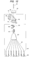
- FIG. 12 is another embodiment of the present invention.
- This example is an example that uses a laser diode device in which a plurality of laser parts are integrated.
- DFB lasers 600 are integrated in the form of an array, optical outputs of the respective lasers are multiplexed into a single waveguide by a multiplexer 602 after passing through waveguides 601, and the optical outputs are restored to a desired optical output by a semiconductor amplifier 603, regaining losses of the optical outputs hitherto being experienced. Then, this light arrives at an exit facet 604 through the electro absorbing modulator 301 equipped with the thin film heater 302. Subsequently, the light becomes a divergent light beam, is focused by the collimator lens 101, passes through the optical isolator 102, is transmitted through the beam splitter 106, and is focused onto the optical fiber 104 with the converging lens 103 to travel therein for information transmission.
- Reflected light from the beam splitter 106 arrives at the photo detector 109 via the etalon or the dielectric multi-layer filter 108.
- a point that differentiates the present invention from the conventional configuration is that the optical isolator 102 is arranged between the beam splitter 106 and the collimator lens 105. With such a configuration, the returned light from the etalon 108 by reflection is blocked by the optical isolator 102 and no resonator is formed externally; therefore no ringing occurs at the photo detector 109.
- just behind the DFB lasers arranged are waveguide photo detectors 605, which are for monitoring the respective outputs of the DFB lasers.
- the embodiment of the wavelength locking optical system described above uses the etalon as the wavelength deviation detection filter by way of example, but in stead of the etalon, a dielectric multi-layer filter can be used.
- polarization controlling elements are employed to suppress the resonance between the dielectric filter and the facet of the laser diode.
- a second form of the present invention is, in an optical module wherein a divergent light beam guided, directly or indirectly, from the rear or the front of a laser source or a light source in which the said tunable laser source and a modulator are integrated is focused with a lens, a wavelength filter is arranged in an optical path of the said focused light beam, there is provided optical path dividing means for dividing transmitted light or reflected light of the said wavelength filter, and there is provided means that guides the said divided light beams to a plurality of photo detectors, detects a quantity of the lasing wavelength shift of the said laser source with the use of difference of photo currents flowing in the respective photo detectors, and controls the wavelength of the said laser source so that the said difference of the photo currents is kept at a constant value, a laser diode module and an application device in which the laser diode module is employed according to the above-mentioned first form, characterized in that a wave plate is arranged in the optical path of the said focused light beam.
- a fourth form of the present invention is, in an optical module wherein a divergent light beam guided, directly or indirectly, from the rear or the front of a laser source or a light source in which the said tunable laser source and a modulator are integrated is focused with a lens, a wavelength filter is arranged in an optical path of the said focused light beam, there is provided optical path dividing means for dividing transmitted light or reflected light of the said wavelength filter, and there is provided means that guides the said divided light beams to a plurality of photo detectors, detects a quantity of the lasing wavelength shift of the said laser source with the use of difference of photo currents flowing in the respective photo detectors, and controls the wavelength of the said laser source so that the said difference of the photo currents is kept at a constant value, a laser diode module and an application device in which the laser diode module is employed according to the above-mentioned first form, characterized in that the wave plate arranged in the optical path of the said focused light beam doubles as light beam dividing means.
- a ninth form of the present invention is a laser diode module and an application device in which the laser diode module is employed according to the above-mentioned first form, characterized in that a plurality of laser sources each having the said laser wavelength controlling means are arranged side by side and there is provided means that combines tunable wavelength ranges covered by respective laser sources.
- a tenth form of the present invention is a laser diode module and an application device in which the laser diode module is employed according to the above-mentioned first form, characterized in that part of or all of the said laser wavelength controlling means is built into a package of the laser source module.
- An eleventh form of the present invention is a laser diode module and an application device in which the laser diode module is employed, comprising at least: a laser diode device; a first photo detector part for receiving, directly or indirectly, first divided light that is a first portion of light when at least one of light emissions of the said laser diode device is divided into two portions of light each traveling a different optical path; a second photo detector for receiving said second divided light that is a second portion of light thus divided via at least a wavelength selective member; and means for controlling the lasing wavelength of the said laser diode device on the basis of outputs of the above-mentioned first and second photo detector parts, and characterized in that superposition between a beam of the light emission from the above-mentioned laser diode device and a beam of the reflected light from a reflecting substance in the optical path between the above-mentioned laser diode device and the above-mentioned wavelength selective member is smaller than superposition of the beams at a parallel reflection plane.
- stabilization of the wavelength of the laser diode namely, stabilization of a wavelength locking optical system in the laser diode module comprising the said wavelength locking optical system can be achieved.
Landscapes
- Physics & Mathematics (AREA)
- Condensed Matter Physics & Semiconductors (AREA)
- General Physics & Mathematics (AREA)
- Electromagnetism (AREA)
- Optics & Photonics (AREA)
- Semiconductor Lasers (AREA)
Applications Claiming Priority (3)
| Application Number | Priority Date | Filing Date | Title |
|---|---|---|---|
| JP2001050534A JP2002252413A (ja) | 2001-02-26 | 2001-02-26 | 半導体レーザモジュール及びこれを用いた光システム |
| JP2001050534 | 2001-02-26 | ||
| US09/934,562 US6597712B2 (en) | 2001-02-26 | 2001-08-23 | Laser diode module |
Publications (3)
| Publication Number | Publication Date |
|---|---|
| EP1235316A2 true EP1235316A2 (de) | 2002-08-28 |
| EP1235316A3 EP1235316A3 (de) | 2004-06-09 |
| EP1235316B1 EP1235316B1 (de) | 2006-07-12 |
Family
ID=26610109
Family Applications (1)
| Application Number | Title | Priority Date | Filing Date |
|---|---|---|---|
| EP01119720A Expired - Lifetime EP1235316B1 (de) | 2001-02-26 | 2001-08-24 | Diodenlasermodul |
Country Status (3)
| Country | Link |
|---|---|
| US (1) | US6983000B2 (de) |
| EP (1) | EP1235316B1 (de) |
| JP (1) | JP2002252413A (de) |
Families Citing this family (12)
| Publication number | Priority date | Publication date | Assignee | Title |
|---|---|---|---|---|
| JP2008016698A (ja) * | 2006-07-07 | 2008-01-24 | Sony Corp | レーザ光源システムおよびレーザ光源の制御方法 |
| JP2008053555A (ja) | 2006-08-25 | 2008-03-06 | Fujitsu Ltd | 波長ロッカー |
| EP2365773B1 (de) | 2008-11-18 | 2019-06-12 | Stryker Corporation | Endoskop-led-lichtquelle mit einem rückkopplungssteuerungssystem |
| US9793673B2 (en) * | 2011-06-13 | 2017-10-17 | Kla-Tencor Corporation | Semiconductor inspection and metrology system using laser pulse multiplier |
| JP2013115257A (ja) * | 2011-11-29 | 2013-06-10 | Mitsubishi Electric Corp | 光モジュール |
| EP2967299B1 (de) | 2013-03-15 | 2022-11-30 | Stryker Corporation | Endoskopische lichtquelle und bildgebungssystem |
| JP6244672B2 (ja) * | 2013-06-04 | 2017-12-13 | 富士通オプティカルコンポーネンツ株式会社 | 光源モジュール、および光送受信装置 |
| WO2017031072A1 (en) * | 2015-08-14 | 2017-02-23 | Skorpios Technologies, Inc. | Broadband high-speed wavelength-division multiplexed receiver using multiple photodetectors per channel |
| JP2017168545A (ja) * | 2016-03-15 | 2017-09-21 | 富士通株式会社 | 光モジュール |
| US10690904B2 (en) | 2016-04-12 | 2020-06-23 | Stryker Corporation | Multiple imaging modality light source |
| US11283237B2 (en) | 2019-07-22 | 2022-03-22 | Coherent, Inc. | Laser wavelength stabilization apparatus |
| CN114777822B (zh) * | 2022-04-18 | 2024-03-19 | 南京大学 | 基于多波长可调谐激光器的光纤光栅阵列同步传感系统 |
Family Cites Families (24)
| Publication number | Priority date | Publication date | Assignee | Title |
|---|---|---|---|---|
| US4583228A (en) * | 1983-11-21 | 1986-04-15 | At&T Bell Laboratories | Frequency stabilization of lasers |
| JPS60117694A (ja) * | 1983-11-30 | 1985-06-25 | Fujitsu Ltd | 光周波数安定化装置 |
| GB2268323B (en) * | 1989-03-30 | 1994-03-23 | Toshiba Kk | Semiconductor laser apparatus |
| JP2546388B2 (ja) * | 1989-08-31 | 1996-10-23 | 日本電気株式会社 | 半導体レーザ装置の発振周波数安定化装置 |
| US5181080A (en) * | 1991-12-23 | 1993-01-19 | Therma-Wave, Inc. | Method and apparatus for evaluating the thickness of thin films |
| NO932088L (no) * | 1993-06-08 | 1995-01-05 | Oddbjoern Gjelsnes | Anordning for anvendelse ved væskeströmscytometri |
| JPH0818145A (ja) * | 1994-04-28 | 1996-01-19 | Olympus Optical Co Ltd | 波長安定化装置 |
| JPH07302948A (ja) * | 1994-05-02 | 1995-11-14 | Olympus Optical Co Ltd | 波長安定化装置 |
| US5519679A (en) * | 1994-10-12 | 1996-05-21 | Eastman Kodak Company | Apparatus and method for multi-spot sampled tracking in an optical data storage system |
| US5949562A (en) * | 1994-11-30 | 1999-09-07 | Canon Kabushiki Kaisha | Transmission wavelength control method permitting efficient wavelength multiplexing, optical communication method, optical transmitter, optical transmitter-receiver apparatus, and optical communication system |
| US5561655A (en) * | 1994-12-02 | 1996-10-01 | Eastman Kodak Company | Apparatus and method for differential tracking in a magneto-optic data storage system using mark edge detection |
| US5790242A (en) * | 1995-07-31 | 1998-08-04 | Robotic Vision Systems, Inc. | Chromatic optical ranging sensor |
| JP3274605B2 (ja) * | 1996-05-01 | 2002-04-15 | 日本無線株式会社 | 炭素同位体分析装置 |
| JP2871623B2 (ja) * | 1996-07-11 | 1999-03-17 | 日本電気株式会社 | 半導体レーザ装置 |
| US5825792A (en) | 1996-07-11 | 1998-10-20 | Northern Telecom Limited | Wavelength monitoring and control assembly for WDM optical transmission systems |
| US6097741A (en) * | 1998-02-17 | 2000-08-01 | Calmar Optcom, Inc. | Passively mode-locked fiber lasers |
| US6046968A (en) * | 1997-07-24 | 2000-04-04 | Hewlett-Packard Company | Re-writable optical disk having reference clock information permanently formed on the disk |
| US6289028B1 (en) * | 1998-02-19 | 2001-09-11 | Uniphase Telecommunications Products, Inc. | Method and apparatus for monitoring and control of laser emission wavelength |
| US6134253A (en) * | 1998-02-19 | 2000-10-17 | Jds Uniphase Corporation | Method and apparatus for monitoring and control of laser emission wavelength |
| GB2336050B (en) * | 1998-03-31 | 2003-03-26 | Marconi Gec Ltd | Improvements in or relating to remote air detection |
| DE19827699A1 (de) * | 1998-06-22 | 1999-12-23 | Siemens Ag | Wellenlängenstabilisierte Laseranordnung |
| JP2000056185A (ja) * | 1998-08-07 | 2000-02-25 | Nippon Telegr & Teleph Corp <Ntt> | レーザダイオードモジュール |
| JP2001325745A (ja) * | 2000-05-16 | 2001-11-22 | Sony Corp | 光学記録媒体と、その再生装置および記録再生装置 |
| US6597712B2 (en) * | 2001-02-26 | 2003-07-22 | Hitachi, Ltd. | Laser diode module |
-
2001
- 2001-02-26 JP JP2001050534A patent/JP2002252413A/ja active Pending
- 2001-08-24 EP EP01119720A patent/EP1235316B1/de not_active Expired - Lifetime
-
2003
- 2003-07-15 US US10/618,759 patent/US6983000B2/en not_active Expired - Fee Related
Also Published As
| Publication number | Publication date |
|---|---|
| EP1235316B1 (de) | 2006-07-12 |
| US20040228373A1 (en) | 2004-11-18 |
| JP2002252413A (ja) | 2002-09-06 |
| US6983000B2 (en) | 2006-01-03 |
| EP1235316A3 (de) | 2004-06-09 |
Similar Documents
| Publication | Publication Date | Title |
|---|---|---|
| US6597712B2 (en) | Laser diode module | |
| EP1156563B1 (de) | Wellenlängenstabilisierung für Laser in optischen Kommunikationssystemen | |
| US6233263B1 (en) | Monitoring and control assembly for wavelength stabilized optical system | |
| US6665321B1 (en) | Tunable laser operation with locally commensurate condition | |
| US7257142B2 (en) | Semi-integrated designs for external cavity tunable lasers | |
| US5651018A (en) | Wavelength-stabilized, high power semiconductor laser | |
| US6757499B1 (en) | Optical transmitter and optical signal transmitter | |
| US6611546B1 (en) | Optical transmitter comprising a stepwise tunable laser | |
| EP1897189B1 (de) | Integrierte überwachungs- und rückkopplungskonstruktionen für abstimmbare laser mit externem resonator | |
| US20040071181A1 (en) | Retro-reflective etalon and the devices using the same | |
| US20040165641A1 (en) | Optical transmitter comprising a stepwise tunable laser | |
| US6801553B2 (en) | Wavelength monitor and semiconductor laser device | |
| EP1235316B1 (de) | Diodenlasermodul | |
| US6937628B2 (en) | Optical transmitter modules | |
| US9634466B2 (en) | External-cavity type laser with built-in wavemeter | |
| US6661818B1 (en) | Etalon, a wavelength monitor/locker using the etalon and associated methods | |
| WO2008150728A1 (en) | A semiconductor optical amplifier for an external cavity diode laser | |
| JP4084006B2 (ja) | 半導体レーザ制御モジュールとその応用装置 | |
| JP6902749B2 (ja) | 波長可変レーザ装置および波長可変レーザの制御方法 | |
| US20050111498A1 (en) | Mode behavior of single-mode semiconductor lasers | |
| US9819149B2 (en) | Optical transmitter implementing wavelength tunable diode | |
| US20060140569A1 (en) | Planar waveguides with air thin films used as anti-reflective layers, beam splitters and mirrors | |
| WO2002025782A2 (en) | Optical transmitter comprising a stepwise tunable laser | |
| JP2010212700A (ja) | 光伝送装置 | |
| JPH0353575A (ja) | 波長安定半導体レーザ |
Legal Events
| Date | Code | Title | Description |
|---|---|---|---|
| PUAI | Public reference made under article 153(3) epc to a published international application that has entered the european phase |
Free format text: ORIGINAL CODE: 0009012 |
|
| AK | Designated contracting states |
Kind code of ref document: A2 Designated state(s): AT BE CH CY DE DK ES FI FR GB GR IE IT LI LU MC NL PT SE TR |
|
| AX | Request for extension of the european patent |
Free format text: AL;LT;LV;MK;RO;SI |
|
| PUAL | Search report despatched |
Free format text: ORIGINAL CODE: 0009013 |
|
| AK | Designated contracting states |
Kind code of ref document: A3 Designated state(s): AT BE CH CY DE DK ES FI FR GB GR IE IT LI LU MC NL PT SE TR |
|
| AX | Request for extension of the european patent |
Extension state: AL LT LV MK RO SI |
|
| 17P | Request for examination filed |
Effective date: 20041011 |
|
| 17Q | First examination report despatched |
Effective date: 20041115 |
|
| AKX | Designation fees paid |
Designated state(s): DE FR GB |
|
| RAP1 | Party data changed (applicant data changed or rights of an application transferred) |
Owner name: HITACHI, LTD. |
|
| RAP1 | Party data changed (applicant data changed or rights of an application transferred) |
Owner name: OPNEXT JAPAN, INC. |
|
| GRAP | Despatch of communication of intention to grant a patent |
Free format text: ORIGINAL CODE: EPIDOSNIGR1 |
|
| GRAS | Grant fee paid |
Free format text: ORIGINAL CODE: EPIDOSNIGR3 |
|
| GRAA | (expected) grant |
Free format text: ORIGINAL CODE: 0009210 |
|
| AK | Designated contracting states |
Kind code of ref document: B1 Designated state(s): DE FR GB |
|
| REG | Reference to a national code |
Ref country code: GB Ref legal event code: FG4D |
|
| REF | Corresponds to: |
Ref document number: 60121416 Country of ref document: DE Date of ref document: 20060824 Kind code of ref document: P |
|
| PG25 | Lapsed in a contracting state [announced via postgrant information from national office to epo] |
Ref country code: DE Free format text: LAPSE BECAUSE OF FAILURE TO SUBMIT A TRANSLATION OF THE DESCRIPTION OR TO PAY THE FEE WITHIN THE PRESCRIBED TIME-LIMIT Effective date: 20061013 |
|
| EN | Fr: translation not filed | ||
| PLBE | No opposition filed within time limit |
Free format text: ORIGINAL CODE: 0009261 |
|
| STAA | Information on the status of an ep patent application or granted ep patent |
Free format text: STATUS: NO OPPOSITION FILED WITHIN TIME LIMIT |
|
| 26N | No opposition filed |
Effective date: 20070413 |
|
| GBPC | Gb: european patent ceased through non-payment of renewal fee |
Effective date: 20061012 |
|
| PG25 | Lapsed in a contracting state [announced via postgrant information from national office to epo] |
Ref country code: GB Free format text: LAPSE BECAUSE OF NON-PAYMENT OF DUE FEES Effective date: 20061012 |
|
| PG25 | Lapsed in a contracting state [announced via postgrant information from national office to epo] |
Ref country code: FR Free format text: LAPSE BECAUSE OF FAILURE TO SUBMIT A TRANSLATION OF THE DESCRIPTION OR TO PAY THE FEE WITHIN THE PRESCRIBED TIME-LIMIT Effective date: 20070511 |
|
| PG25 | Lapsed in a contracting state [announced via postgrant information from national office to epo] |
Ref country code: FR Free format text: LAPSE BECAUSE OF FAILURE TO SUBMIT A TRANSLATION OF THE DESCRIPTION OR TO PAY THE FEE WITHIN THE PRESCRIBED TIME-LIMIT Effective date: 20060712 |