EP1233398A2 - Organic electroluminecent pixel circuit - Google Patents
Organic electroluminecent pixel circuit Download PDFInfo
- Publication number
- EP1233398A2 EP1233398A2 EP02251010A EP02251010A EP1233398A2 EP 1233398 A2 EP1233398 A2 EP 1233398A2 EP 02251010 A EP02251010 A EP 02251010A EP 02251010 A EP02251010 A EP 02251010A EP 1233398 A2 EP1233398 A2 EP 1233398A2
- Authority
- EP
- European Patent Office
- Prior art keywords
- organic
- pixel
- transistor
- pixels
- gate line
- Prior art date
- Legal status (The legal status is an assumption and is not a legal conclusion. Google has not performed a legal analysis and makes no representation as to the accuracy of the status listed.)
- Withdrawn
Links
Images




Classifications
-
- G—PHYSICS
- G09—EDUCATION; CRYPTOGRAPHY; DISPLAY; ADVERTISING; SEALS
- G09G—ARRANGEMENTS OR CIRCUITS FOR CONTROL OF INDICATING DEVICES USING STATIC MEANS TO PRESENT VARIABLE INFORMATION
- G09G3/00—Control arrangements or circuits, of interest only in connection with visual indicators other than cathode-ray tubes
- G09G3/20—Control arrangements or circuits, of interest only in connection with visual indicators other than cathode-ray tubes for presentation of an assembly of a number of characters, e.g. a page, by composing the assembly by combination of individual elements arranged in a matrix no fixed position being assigned to or needed to be assigned to the individual characters or partial characters
- G09G3/22—Control arrangements or circuits, of interest only in connection with visual indicators other than cathode-ray tubes for presentation of an assembly of a number of characters, e.g. a page, by composing the assembly by combination of individual elements arranged in a matrix no fixed position being assigned to or needed to be assigned to the individual characters or partial characters using controlled light sources
- G09G3/30—Control arrangements or circuits, of interest only in connection with visual indicators other than cathode-ray tubes for presentation of an assembly of a number of characters, e.g. a page, by composing the assembly by combination of individual elements arranged in a matrix no fixed position being assigned to or needed to be assigned to the individual characters or partial characters using controlled light sources using electroluminescent panels
-
- G—PHYSICS
- G09—EDUCATION; CRYPTOGRAPHY; DISPLAY; ADVERTISING; SEALS
- G09G—ARRANGEMENTS OR CIRCUITS FOR CONTROL OF INDICATING DEVICES USING STATIC MEANS TO PRESENT VARIABLE INFORMATION
- G09G3/00—Control arrangements or circuits, of interest only in connection with visual indicators other than cathode-ray tubes
- G09G3/20—Control arrangements or circuits, of interest only in connection with visual indicators other than cathode-ray tubes for presentation of an assembly of a number of characters, e.g. a page, by composing the assembly by combination of individual elements arranged in a matrix no fixed position being assigned to or needed to be assigned to the individual characters or partial characters
- G09G3/22—Control arrangements or circuits, of interest only in connection with visual indicators other than cathode-ray tubes for presentation of an assembly of a number of characters, e.g. a page, by composing the assembly by combination of individual elements arranged in a matrix no fixed position being assigned to or needed to be assigned to the individual characters or partial characters using controlled light sources
- G09G3/30—Control arrangements or circuits, of interest only in connection with visual indicators other than cathode-ray tubes for presentation of an assembly of a number of characters, e.g. a page, by composing the assembly by combination of individual elements arranged in a matrix no fixed position being assigned to or needed to be assigned to the individual characters or partial characters using controlled light sources using electroluminescent panels
- G09G3/32—Control arrangements or circuits, of interest only in connection with visual indicators other than cathode-ray tubes for presentation of an assembly of a number of characters, e.g. a page, by composing the assembly by combination of individual elements arranged in a matrix no fixed position being assigned to or needed to be assigned to the individual characters or partial characters using controlled light sources using electroluminescent panels semiconductive, e.g. using light-emitting diodes [LED]
- G09G3/3208—Control arrangements or circuits, of interest only in connection with visual indicators other than cathode-ray tubes for presentation of an assembly of a number of characters, e.g. a page, by composing the assembly by combination of individual elements arranged in a matrix no fixed position being assigned to or needed to be assigned to the individual characters or partial characters using controlled light sources using electroluminescent panels semiconductive, e.g. using light-emitting diodes [LED] organic, e.g. using organic light-emitting diodes [OLED]
- G09G3/3225—Control arrangements or circuits, of interest only in connection with visual indicators other than cathode-ray tubes for presentation of an assembly of a number of characters, e.g. a page, by composing the assembly by combination of individual elements arranged in a matrix no fixed position being assigned to or needed to be assigned to the individual characters or partial characters using controlled light sources using electroluminescent panels semiconductive, e.g. using light-emitting diodes [LED] organic, e.g. using organic light-emitting diodes [OLED] using an active matrix
- G09G3/3258—Control arrangements or circuits, of interest only in connection with visual indicators other than cathode-ray tubes for presentation of an assembly of a number of characters, e.g. a page, by composing the assembly by combination of individual elements arranged in a matrix no fixed position being assigned to or needed to be assigned to the individual characters or partial characters using controlled light sources using electroluminescent panels semiconductive, e.g. using light-emitting diodes [LED] organic, e.g. using organic light-emitting diodes [OLED] using an active matrix with pixel circuitry controlling the voltage across the light-emitting element
-
- G—PHYSICS
- G09—EDUCATION; CRYPTOGRAPHY; DISPLAY; ADVERTISING; SEALS
- G09G—ARRANGEMENTS OR CIRCUITS FOR CONTROL OF INDICATING DEVICES USING STATIC MEANS TO PRESENT VARIABLE INFORMATION
- G09G2300/00—Aspects of the constitution of display devices
- G09G2300/04—Structural and physical details of display devices
- G09G2300/0439—Pixel structures
- G09G2300/0465—Improved aperture ratio, e.g. by size reduction of the pixel circuit, e.g. for improving the pixel density or the maximum displayable luminance or brightness
-
- G—PHYSICS
- G09—EDUCATION; CRYPTOGRAPHY; DISPLAY; ADVERTISING; SEALS
- G09G—ARRANGEMENTS OR CIRCUITS FOR CONTROL OF INDICATING DEVICES USING STATIC MEANS TO PRESENT VARIABLE INFORMATION
- G09G2300/00—Aspects of the constitution of display devices
- G09G2300/08—Active matrix structure, i.e. with use of active elements, inclusive of non-linear two terminal elements, in the pixels together with light emitting or modulating elements
- G09G2300/0809—Several active elements per pixel in active matrix panels
-
- G—PHYSICS
- G09—EDUCATION; CRYPTOGRAPHY; DISPLAY; ADVERTISING; SEALS
- G09G—ARRANGEMENTS OR CIRCUITS FOR CONTROL OF INDICATING DEVICES USING STATIC MEANS TO PRESENT VARIABLE INFORMATION
- G09G2300/00—Aspects of the constitution of display devices
- G09G2300/08—Active matrix structure, i.e. with use of active elements, inclusive of non-linear two terminal elements, in the pixels together with light emitting or modulating elements
- G09G2300/0809—Several active elements per pixel in active matrix panels
- G09G2300/0842—Several active elements per pixel in active matrix panels forming a memory circuit, e.g. a dynamic memory with one capacitor
-
- G—PHYSICS
- G09—EDUCATION; CRYPTOGRAPHY; DISPLAY; ADVERTISING; SEALS
- G09G—ARRANGEMENTS OR CIRCUITS FOR CONTROL OF INDICATING DEVICES USING STATIC MEANS TO PRESENT VARIABLE INFORMATION
- G09G2300/00—Aspects of the constitution of display devices
- G09G2300/08—Active matrix structure, i.e. with use of active elements, inclusive of non-linear two terminal elements, in the pixels together with light emitting or modulating elements
- G09G2300/0809—Several active elements per pixel in active matrix panels
- G09G2300/0842—Several active elements per pixel in active matrix panels forming a memory circuit, e.g. a dynamic memory with one capacitor
- G09G2300/0861—Several active elements per pixel in active matrix panels forming a memory circuit, e.g. a dynamic memory with one capacitor with additional control of the display period without amending the charge stored in a pixel memory, e.g. by means of additional select electrodes
-
- G—PHYSICS
- G09—EDUCATION; CRYPTOGRAPHY; DISPLAY; ADVERTISING; SEALS
- G09G—ARRANGEMENTS OR CIRCUITS FOR CONTROL OF INDICATING DEVICES USING STATIC MEANS TO PRESENT VARIABLE INFORMATION
- G09G2310/00—Command of the display device
- G09G2310/02—Addressing, scanning or driving the display screen or processing steps related thereto
- G09G2310/0243—Details of the generation of driving signals
- G09G2310/0251—Precharge or discharge of pixel before applying new pixel voltage
-
- G—PHYSICS
- G09—EDUCATION; CRYPTOGRAPHY; DISPLAY; ADVERTISING; SEALS
- G09G—ARRANGEMENTS OR CIRCUITS FOR CONTROL OF INDICATING DEVICES USING STATIC MEANS TO PRESENT VARIABLE INFORMATION
- G09G2310/00—Command of the display device
- G09G2310/02—Addressing, scanning or driving the display screen or processing steps related thereto
- G09G2310/0243—Details of the generation of driving signals
- G09G2310/0254—Control of polarity reversal in general, other than for liquid crystal displays
- G09G2310/0256—Control of polarity reversal in general, other than for liquid crystal displays with the purpose of reversing the voltage across a light emitting or modulating element within a pixel
-
- G—PHYSICS
- G09—EDUCATION; CRYPTOGRAPHY; DISPLAY; ADVERTISING; SEALS
- G09G—ARRANGEMENTS OR CIRCUITS FOR CONTROL OF INDICATING DEVICES USING STATIC MEANS TO PRESENT VARIABLE INFORMATION
- G09G2320/00—Control of display operating conditions
- G09G2320/02—Improving the quality of display appearance
- G09G2320/0257—Reduction of after-image effects
-
- G—PHYSICS
- G09—EDUCATION; CRYPTOGRAPHY; DISPLAY; ADVERTISING; SEALS
- G09G—ARRANGEMENTS OR CIRCUITS FOR CONTROL OF INDICATING DEVICES USING STATIC MEANS TO PRESENT VARIABLE INFORMATION
- G09G2330/00—Aspects of power supply; Aspects of display protection and defect management
- G09G2330/02—Details of power systems and of start or stop of display operation
- G09G2330/021—Power management, e.g. power saving
Definitions
- the present invention relates to an organic EL pixel circuit for controlling application of a drive voltage to an organic EL pixel.
- organic EL panels as flat panel displays has been conventionally known. Because the pixels in an organic EL panel are self-illuminating, an organic EL panel has advantages including that, unlike a liquid crystal display, no backlight is required and that the display is relatively bright.
- Fig. 8 illustrates an example structure of a pixel circuit in an organic EL panel employing conventional thin film transistors (TFTs).
- TFTs thin film transistors
- An organic EL panel is composed of these pixels arranged in a matrix.
- Fig. 8 shows the gate of a selection transistor TFT1, which is an n-channel thin film transistor to be selected by a gate line and which will hereinafter be referred to simply as TFT1, connected to a gate line extending in the row direction.
- the drain of the TFT1 is connected with a data line extending in the column direction.
- the source of the TFT1 is connected with one end of a storage capacitor SC having the other end connected a storage capacitor power source line.
- the node connecting the source of the TFT1 and the storage capacitor SC is connected with the gate of a drive transistor TFT2 which is a p-channel thin film transistor (which will be hereinafter referred to simply as TFT2).
- the source of the TFT2 is connected to a power source PVDD and the drains of the TFT2 is connected with one end of an organic EL element EL.
- the other end of the organic EL element EL is connected with a cathode power source CV.
- the TFT1 when the gate line is at H level, the TFT1 is turned on, and the data in the data line at this point is stored in the storage capacitor SC.
- the TFT2 is switched on and off in accordance with the data (potential) held by the storage capacitor SC.
- an electrical current flows through the organic EL element EL, which then emits light.
- each pixel Light emission of each pixel is controlled in the manner described above. Because of the existence of the storage capacitor SC, the organic EL element EL is capable of emitting light even after the TFT1 is turned off.
- the storage capacitor SC typically retains the ON or OFF state of the TFT2 until the next gate line is selected.
- the pixels arranged in a matrix and each including the organic EL element, TFT1 and TFT2, are disposed on the same substrate. This structure results in generation of a parasitic capacitor in the organic EL element EL.
- such a conventional pixel circuit has a problem that even when the TFT2 is off, a current flows in the organic EL element EL in accordance with the charges accumulated in the capacitor of the organic EL element, thereby generating an afterimage. More specifically, while the panel operates at a high response speed when the organic EL element is turned on, the response becomes slower due to the influence of the capacitor of the organic EL element when the organic EL element is turned off, with a result that afterimages are common.
- the present invention was conceived in view of the aforementioned problems of the prior art and aims to provide an organic EL pixel circuit capable of effectively preventing generation of an afterimage.
- charges which are accumulated in the capacitor of the organic EL element can be discharged by a discharge transistor. Accordingly, it is possible to prevent an afterimage from being generated due to the charges which are accumulated in the capacitor of the organic EL element, thereby preventing the organic EL element from being retained ON when the organic EL element switches OFF.
- the organic EL pixels are arranged in a matrix, the pixels in a row direction are selected by the same gate line, and the discharge transistor is driven by the gate line selected at a timing prior to the selection of the gate line at the row of the EL element to which the discharge transistor is connected, to thereby discharge the charges accumulated in the capacitor of the organic EL element.
- Prevention of afterimage generation can thereby be ensured because the capacitor of the organic EL is thus discharged in advance.
- the discharge transistor is driven by a dedicated discharge line which is activated at a timing prior to the selection of the gate line at the row of the EL element to which said discharge transistor is connected, to discharge the charges accumulated in the capacitor of the organic EL element.
- each pixel includes a storage capacitor for holding a control voltage to be applied to a drive transistor which controls application of a drive current to the organic EL element, and further includes a control transistor for controlling the control voltage held in the storage capacitor to turn the drive transistor off. It is thus possible to turn the drive transistor off by performing discharge using the control transistor.
- control transistor is driven simultaneously with said discharge transistor to turn the drive transistor off at the time of driving said discharge transistor, i.e. when the discharge transistor is turned on. This leads to advantages that the display period is maintained, the wiring is shortened, and prevention of afterimage generation is ensured. Further, a simultaneous ON state of the drive transistor and the discharge transistor can also be prevented.
- control transistor is driven prior to the discharge transistor to thereby turn the drive transistor off prior to driving the discharge transistor. This can further ensure prevention of a simultaneous ON state of the drive transistor and the discharge transistor.
- the organic EL pixels are arranged in a matrix, that each of the pixels emits light of a color which is predetermined for each pixel, and that a discharge transistor and/or a control transistor for a pixel which emits light of a color with low emission efficiency is disposed within a pixel which emits light of a color with high emission efficiency.
- a discharge transistor and/or a control transistor for a pixel which emits light of a color with low emission efficiency is disposed within a pixel which emits light of a color with high emission efficiency.
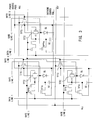
- Fig. 1 illustrates a structure of a pixel circuit corresponding to one pixel portion according to one embodiment of the present invention.
- a TFT1 comprising a n-channel TFT is connected to a gate line extending in the horizontal direction.
- the TFT1 which is formed as a double-gate type TFT having TFTs connected in series in this embodiment, need not necessarily be of the double-gate type.
- the other end of the TFT1 is connected with one end of the storage capacitor SC.
- the other end of the storage capacitor SC is connected with VEE, which is a negative power source of the panel.
- VEE which is a negative power source of the panel.
- the gate of the drive transistor TFT2 comprising a p-channel TFT is connected to the node connecting the TFT1 and the storage capacitor SC.
- the TFT2 which is formed of two TFTs connected in parallel, has one end connected with the panel power source PVDD and the other end connected with one end of the organic EL element EL.
- the other end of the organic EL element is connected with a cathode provided at an opposing substrate.
- one end of a discharge transistor TFT3 having the other end connected with the VEE is connected to the node connecting the TFT2 and the organic EL element.
- the gate of the discharge TFT3 is connected to the upper gate line.
- the gate of the TFT3 is connected to the gate line 0 which is one horizontal line above the gate line 1 to which the TFT1 of the pixel for the TFT3 is connected.
- control transistor TFT4 is connected to the node connecting the TFT1 and the storage capacitor SC.
- the other end of the control transistor TFT4 is connected with the power source PVDD.
- the gate of the control transistor TFT4 is connected with the upper gate line, similarly to the gate of the TFT3 described above.
- the gate lines are sequentially turned on by the vertical driver. Specifically, in displaying one screen defined by a vertical synchronization signal, the gate lines corresponding to the horizontal lines for performing display are sequentially turned on in accordance with the horizontal synchronization signal.
- the data lines are sequentially connected with the video signal line by the horizontal driver, so that data corresponding to each pixel is supplied via the TFT1 to the gate of the TFT2 and the storage capacitor SC. Accordingly, data is basically supplied in a dot sequential manner. The data thus supplied is stored in the storage capacitor, and the ON or OFF state of the TFT2 is maintained thereafter.
- the TFT2 is on, an electrical current flows from the power source PVDD into the organic EL element EL, which then emits light.
- the TFT2 which is a p-channel TFT, turns off when the charges are held in the storage capacitor SC and the gate of the TFT2 is at H level.
- the TFT2 turns on when the charges are discharged and the gate of the TFT2 becomes L level.
- the TFT3 is turned on by the upper gate line.
- the upper side of the organic EL element EL namely the drain of the TFT2
- the negative power source VEE at the time point one horizontal line before the time point for turning the TFT1 on
- the charges accumulated in the capacitor of the organic EL element EL are discharged.
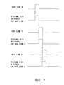
- the TFT4 connected with the TFT1 which is to be turned on by the gate line 1 and the TFT3 connected with the EL are turned on, so that the charges accumulated in the capacitor of the organic EL element EL of each pixel for the gate line 1 are discharged.
- the TFT3 with regard to each of the pixels in the lines for the gate line 2 is turned on, so that the charges accumulated in the organic EL element EL for those pixels are discharged.
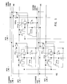
- Fig. 3 illustrates another embodiment, in which the other end of the TFT4 is connected to the gate line which is two lines above the gate line which is being selected, not to the upper gate line.
- the storage capacitor is charged by the PVDD, and the TFT2 is turned off.
- the TFT3 turns on to thereby discharge the capacitor of the organic EL. This structure further ensures the prevention of simultaneous on state of the TFT2 and the TFT3.
- the TFT3 of the pixels for the gate line 1 and the TFT4 of the pixels for the gate line 2 are turned on.
- the gate line 1 is on
- the TFT3 of the pixels for the gate line 2 and the TFT4 of the pixels for the gate line 3 are turned on.
- the TFT4 is first turned on so that the storage capacitor SC is charged to turn the TFT2 off, and subsequently the TFT3 is turned on to discharge the capacitor of the organic EL.
- the TFT1 is turned on so that the data writing is performed.
- the timing at which the TFT3 and the TFT4 are turned on is not necessarily limited to when the upper gate line or the gate line two lines above the selected gate line is actuated, but may be at the actuation of gate lines higher up.
- TFT3 and TFT4 may be turned on at any timing as long as they are actuated by a signal of a gate line which is selected prior to the gate line for those TFT3 and TFT4.
- the TFT4 may be turned on at any timing as long as it is the same as or prior to the timing of actuating the TFT3.
- the provision of the TFT3 can ensure the off state of the organic EL when the organic EL is switched off, thereby preventing the generation of an afterimage. Also, because the TFT4 is further provided, it is possible to prevent the TFT2 from turning on and also prevent the TFT4 from connecting the power source PVDD and the negative power source VEE, when the TFT3 is on.
- the wiring may be drawn from the lowermost gate line or the gate line above the lowermost line.
- a dummy gate line (having no corresponding pixels) which is turned on during the vertical retrace interval may be provided to thereby turn the TFT3 and TFT4 on.
- a discharge gate line dedicated to exclusive use for actuating the TFT3 and TFT4 (hereinafter referred to as a dedicated discharge gate line) is provided, and the gate of the TFT3 and TFT4 at each line is connected with the dedicated discharge gate line at that line.
- each dedicated discharge gate line is turned on (activated) simultaneously with the upper gate line. Therefore, as in the embodiment described in connection with Fig. 1, the TFT3 and TFT4 are turned on at the timing when the upper gate line is turned on.
- the TFT3 and the TFT4 may be connected with separate dedicated discharge gate lines, or one of the TFT3 and TFT4 may be connected to the gate line to thereby turn the TFT3 and TFT4 on at different timing.
- Fig. 7 illustrates a further embodiment in which considerations are made with regard to the locations of the TFT3 and TFT4.
- three pixels are shown; the pixel at upper left corresponds to a R (red) pixel, the pixel at upper right corresponds to a G (green) pixel, and the pixel at lower left corresponds to a B (blue) pixel.
- the arrangement of the RGB pixels is not limited to this example, but may also be, for example, a stripe pattern in which pixels of the same color are arranged in the column direction, or any other suitable pattern.
- the TFT3 and the TFT4 for the R pixel are located within the adjacent G pixel. Therefore, the number of the TFTs provided within the R pixel is smaller than that in the G pixel. Because the aperture ratio of a pixel decreases as the number of TFTs provided in the pixel increases, in this embodiment, the aperture ratio of the R pixel is larger than that of the G pixel.
- the emissive element for G has a high emission efficiency and is therefore relatively bright, while the emissive element for R has a low emission efficiency and is therefore relatively dark.
- Fig. 7 only illustrates an arrangement for a circuit diagram and that the position and size of the individual members or the like may be different from the actual layout. Further, in Fig. 7, the border line between the pixels is shown by dashed line.
- each of the transistors is not limited to that described in the above examples, and may be the opposite. In such case, a signal would have the opposite polarity.
Landscapes
- Engineering & Computer Science (AREA)
- Physics & Mathematics (AREA)
- Computer Hardware Design (AREA)
- General Physics & Mathematics (AREA)
- Theoretical Computer Science (AREA)
- Electroluminescent Light Sources (AREA)
- Control Of Indicators Other Than Cathode Ray Tubes (AREA)
- Control Of El Displays (AREA)
Abstract
Description
Claims (8)
- An organic EL pixel circuit for controlling application of a drive voltage to a plurality of organic EL pixels, wherein a discharge transistor is provided for discharging charges accumulated in a capacitor of an organic EL element.
- An organic EL pixel circuit according to claim 1, wherein
said organic EL pixels are arranged in a matrix and the pixels in a row direction are selected by a same gate line, and
said discharge transistor is driven by a gate line which is selected at a timing prior to the selection of the gate line at the row of the EL element to which said discharge transistor is connected, to discharge the charges accumulated in the capacitor of the organic EL element. - An organic EL pixel circuit according to claim 1, wherein
said organic EL pixels are arranged in a matrix and the pixels in a row direction are selected by a same gate line, and
said discharge transistor is driven by a dedicated discharge line which is activated at a timing prior to the selection of the gate line at the row of the EL element to which said discharge transistor is connected, to discharge the charges accumulated in the capacitor of the organic EL element. - An organic EL pixel circuit according to any one of claims 1 to 3, wherein
said organic EL pixels are arranged in a matrix and each of the pixels emits light of a color which is predetermined for each pixel, and
a discharge transistor for a pixel which emits light of a color with a low emission efficiency is provided within a pixel which emits light of a color with a higher emission efficiency. - An organic EL pixel circuit according to any one of claims 1 to 4, wherein
each of said pixels includes a storage capacitor for holding a control voltage to be applied to a drive transistor which controls application of a drive current to the organic EL element, and
each of said pixels further includes a control transistor for controlling the control voltage held in the storage capacitor to turn the drive transistor off. - An organic EL pixel circuit according to claim 5, wherein
said control transistor is driven simultaneously with said discharge transistor to turn the drive transistor off at the time of driving said discharge transistor. - An organic EL pixel circuit according to claim 5, wherein
said control transistor is driven prior to said discharge transistor to turn the drive transistor off prior to driving of said discharge transistor. - An organic EL pixel circuit according to any one of claims 5 to 7, wherein
said organic EL pixels are arranged in a matrix and each of the pixels emits light of a color which is predetermined for each pixel, and
a control transistor for a pixel which emits light of a color with a lower emission efficiency is provided within a pixel which emits light of a color with a higher emission efficiency.
Applications Claiming Priority (2)
| Application Number | Priority Date | Filing Date | Title |
|---|---|---|---|
| JP2001038642A JP2002244617A (en) | 2001-02-15 | 2001-02-15 | Organic EL pixel circuit |
| JP2001038642 | 2001-02-15 |
Publications (2)
| Publication Number | Publication Date |
|---|---|
| EP1233398A2 true EP1233398A2 (en) | 2002-08-21 |
| EP1233398A3 EP1233398A3 (en) | 2007-02-21 |
Family
ID=18901576
Family Applications (1)
| Application Number | Title | Priority Date | Filing Date |
|---|---|---|---|
| EP02251010A Withdrawn EP1233398A3 (en) | 2001-02-15 | 2002-02-14 | Organic electroluminecent pixel circuit |
Country Status (6)
| Country | Link |
|---|---|
| US (1) | US6924602B2 (en) |
| EP (1) | EP1233398A3 (en) |
| JP (1) | JP2002244617A (en) |
| KR (1) | KR20020067678A (en) |
| CN (1) | CN100423058C (en) |
| TW (1) | TW552574B (en) |
Cited By (3)
| Publication number | Priority date | Publication date | Assignee | Title |
|---|---|---|---|---|
| WO2004061812A1 (en) * | 2002-12-27 | 2004-07-22 | Semiconductor Energy Laboratory Co., Ltd. | Semiconductor device and display device using the same |
| EP1429311A3 (en) * | 2002-11-21 | 2007-12-26 | Pioneer Corporation | Display controller, display system, and display controlling method |
| US8477085B2 (en) | 2006-12-15 | 2013-07-02 | Semiconductor Energy Laboratory Co., Ltd. | Semiconductor device and driving method thereof |
Families Citing this family (114)
| Publication number | Priority date | Publication date | Assignee | Title |
|---|---|---|---|---|
| KR100488835B1 (en) * | 2002-04-04 | 2005-05-11 | 산요덴키가부시키가이샤 | Semiconductor device and display device |
| TW571281B (en) * | 2002-09-12 | 2004-01-11 | Au Optronics Corp | Driving circuit and method for a display device and display device therewith |
| KR100539529B1 (en) * | 2002-09-24 | 2005-12-30 | 엘지전자 주식회사 | circuit for driving of organic Electro-Luminescence display |
| KR100906964B1 (en) * | 2002-09-25 | 2009-07-08 | 삼성전자주식회사 | Organic electroluminescent drive device and organic electroluminescent display panel having same |
| JP2004117820A (en) * | 2002-09-26 | 2004-04-15 | Seiko Epson Corp | Electronic circuits, electronic devices and electronic equipment |
| JP3985667B2 (en) * | 2002-11-22 | 2007-10-03 | ソニー株式会社 | Electrochemical display device and driving method |
| KR20040087427A (en) * | 2003-04-07 | 2004-10-14 | 삼성전자주식회사 | Organic electro-luminescent panel and organic electro-luminescent display device |
| TWI250496B (en) * | 2003-06-20 | 2006-03-01 | Au Optronics Corp | Driving method for current driven active matrix organic light emitting diode pixel |
| KR100560780B1 (en) * | 2003-07-07 | 2006-03-13 | 삼성에스디아이 주식회사 | Pixel circuit of organic light emitting display device and driving method thereof |
| JP3987824B2 (en) * | 2003-09-12 | 2007-10-10 | 勝華科技股▲ふん▼有限公司 | Driving circuit and driving method for active matrix organic EL display |
| CA2443206A1 (en) | 2003-09-23 | 2005-03-23 | Ignis Innovation Inc. | Amoled display backplanes - pixel driver circuits, array architecture, and external compensation |
| JP4338131B2 (en) | 2003-09-30 | 2009-10-07 | インターナショナル・ビジネス・マシーンズ・コーポレーション | TFT array, display panel, and inspection method of TFT array |
| KR100607513B1 (en) * | 2003-11-25 | 2006-08-02 | 엘지.필립스 엘시디 주식회사 | Electro-luminescence display and its driving method |
| KR100568592B1 (en) * | 2003-12-30 | 2006-04-07 | 엘지.필립스 엘시디 주식회사 | Electro-luminescence display and its driving method |
| KR100568596B1 (en) * | 2004-03-25 | 2006-04-07 | 엘지.필립스 엘시디 주식회사 | Electro-luminescence display and its driving method |
| KR101076424B1 (en) * | 2004-03-31 | 2011-10-25 | 엘지디스플레이 주식회사 | Method and apparatus for precharging electro luminescence panel |
| US6977470B2 (en) * | 2004-04-28 | 2005-12-20 | Au Optronics Corp. | Current-driven OLED pixel |
| CA2472671A1 (en) | 2004-06-29 | 2005-12-29 | Ignis Innovation Inc. | Voltage-programming scheme for current-driven amoled displays |
| US7336269B2 (en) * | 2004-09-24 | 2008-02-26 | Chunghwa Picture Tubes, Ltd. | Electronic discharging control circuit and method thereof for LCD |
| CA2490858A1 (en) | 2004-12-07 | 2006-06-07 | Ignis Innovation Inc. | Driving method for compensated voltage-programming of amoled displays |
| US10012678B2 (en) | 2004-12-15 | 2018-07-03 | Ignis Innovation Inc. | Method and system for programming, calibrating and/or compensating, and driving an LED display |
| US20140111567A1 (en) | 2005-04-12 | 2014-04-24 | Ignis Innovation Inc. | System and method for compensation of non-uniformities in light emitting device displays |
| US9275579B2 (en) | 2004-12-15 | 2016-03-01 | Ignis Innovation Inc. | System and methods for extraction of threshold and mobility parameters in AMOLED displays |
| US10013907B2 (en) | 2004-12-15 | 2018-07-03 | Ignis Innovation Inc. | Method and system for programming, calibrating and/or compensating, and driving an LED display |
| US9280933B2 (en) | 2004-12-15 | 2016-03-08 | Ignis Innovation Inc. | System and methods for extraction of threshold and mobility parameters in AMOLED displays |
| US9799246B2 (en) | 2011-05-20 | 2017-10-24 | Ignis Innovation Inc. | System and methods for extraction of threshold and mobility parameters in AMOLED displays |
| US9171500B2 (en) | 2011-05-20 | 2015-10-27 | Ignis Innovation Inc. | System and methods for extraction of parasitic parameters in AMOLED displays |
| US8576217B2 (en) | 2011-05-20 | 2013-11-05 | Ignis Innovation Inc. | System and methods for extraction of threshold and mobility parameters in AMOLED displays |
| US8599191B2 (en) | 2011-05-20 | 2013-12-03 | Ignis Innovation Inc. | System and methods for extraction of threshold and mobility parameters in AMOLED displays |
| TWI402790B (en) | 2004-12-15 | 2013-07-21 | 伊格尼斯創新股份有限公司 | Method and system for programming, calibrating and driving a light-emitting element display |
| CA2496642A1 (en) | 2005-02-10 | 2006-08-10 | Ignis Innovation Inc. | Fast settling time driving method for organic light-emitting diode (oled) displays based on current programming |
| US7852298B2 (en) | 2005-06-08 | 2010-12-14 | Ignis Innovation Inc. | Method and system for driving a light emitting device display |
| CA2518276A1 (en) | 2005-09-13 | 2007-03-13 | Ignis Innovation Inc. | Compensation technique for luminance degradation in electro-luminance devices |
| US20070063192A1 (en) * | 2005-09-20 | 2007-03-22 | Toppoly Optoelectronics Corp. | Systems for emitting light incorporating pixel structures of organic light-emitting diodes |
| US9489891B2 (en) | 2006-01-09 | 2016-11-08 | Ignis Innovation Inc. | Method and system for driving an active matrix display circuit |
| US9269322B2 (en) | 2006-01-09 | 2016-02-23 | Ignis Innovation Inc. | Method and system for driving an active matrix display circuit |
| EP2458579B1 (en) | 2006-01-09 | 2017-09-20 | Ignis Innovation Inc. | Method and system for driving an active matrix display circuit |
| TW200746022A (en) | 2006-04-19 | 2007-12-16 | Ignis Innovation Inc | Stable driving scheme for active matrix displays |
| TWI371018B (en) * | 2006-05-09 | 2012-08-21 | Chimei Innolux Corp | System for displaying image and driving display element method |
| CA2556961A1 (en) | 2006-08-15 | 2008-02-15 | Ignis Innovation Inc. | Oled compensation technique based on oled capacitance |
| KR100824854B1 (en) | 2006-12-21 | 2008-04-23 | 삼성에스디아이 주식회사 | Organic electroluminescent display |
| KR100833756B1 (en) * | 2007-01-15 | 2008-05-29 | 삼성에스디아이 주식회사 | Organic electroluminescent display |
| KR101375040B1 (en) * | 2007-03-22 | 2014-03-14 | 엘지디스플레이 주식회사 | Pixel circuit display panel having the same |
| JP2009014796A (en) * | 2007-06-30 | 2009-01-22 | Sony Corp | El display panel, power supply line driving device and electronic equipment |
| KR100889690B1 (en) * | 2007-08-28 | 2009-03-19 | 삼성모바일디스플레이주식회사 | DC-DC converter and organic light emitting display device using the same |
| WO2009127065A1 (en) | 2008-04-18 | 2009-10-22 | Ignis Innovation Inc. | System and driving method for light emitting device display |
| KR20100009219A (en) | 2008-07-18 | 2010-01-27 | 삼성모바일디스플레이주식회사 | Pixel and organic light emitting display device using the same |
| CA2637343A1 (en) | 2008-07-29 | 2010-01-29 | Ignis Innovation Inc. | Improving the display source driver |
| US9370075B2 (en) | 2008-12-09 | 2016-06-14 | Ignis Innovation Inc. | System and method for fast compensation programming of pixels in a display |
| KR101499236B1 (en) * | 2008-12-29 | 2015-03-06 | 삼성디스플레이 주식회사 | Display device and driving method thereof |
| JP5458582B2 (en) * | 2009-01-28 | 2014-04-02 | ソニー株式会社 | Solid-state imaging device, driving method of solid-state imaging device, and electronic apparatus |
| US9384698B2 (en) | 2009-11-30 | 2016-07-05 | Ignis Innovation Inc. | System and methods for aging compensation in AMOLED displays |
| US9311859B2 (en) | 2009-11-30 | 2016-04-12 | Ignis Innovation Inc. | Resetting cycle for aging compensation in AMOLED displays |
| CA2669367A1 (en) | 2009-06-16 | 2010-12-16 | Ignis Innovation Inc | Compensation technique for color shift in displays |
| CA2688870A1 (en) | 2009-11-30 | 2011-05-30 | Ignis Innovation Inc. | Methode and techniques for improving display uniformity |
| US10319307B2 (en) | 2009-06-16 | 2019-06-11 | Ignis Innovation Inc. | Display system with compensation techniques and/or shared level resources |
| US8283967B2 (en) | 2009-11-12 | 2012-10-09 | Ignis Innovation Inc. | Stable current source for system integration to display substrate |
| US10996258B2 (en) | 2009-11-30 | 2021-05-04 | Ignis Innovation Inc. | Defect detection and correction of pixel circuits for AMOLED displays |
| US10867536B2 (en) | 2013-04-22 | 2020-12-15 | Ignis Innovation Inc. | Inspection system for OLED display panels |
| US8803417B2 (en) | 2009-12-01 | 2014-08-12 | Ignis Innovation Inc. | High resolution pixel architecture |
| CA2687631A1 (en) | 2009-12-06 | 2011-06-06 | Ignis Innovation Inc | Low power driving scheme for display applications |
| KR101117729B1 (en) * | 2009-12-17 | 2012-03-07 | 삼성모바일디스플레이주식회사 | Pixel circuit, and organic light emitting display and method for controlling a brightness thereof |
| US10163401B2 (en) | 2010-02-04 | 2018-12-25 | Ignis Innovation Inc. | System and methods for extracting correlation curves for an organic light emitting device |
| US10176736B2 (en) | 2010-02-04 | 2019-01-08 | Ignis Innovation Inc. | System and methods for extracting correlation curves for an organic light emitting device |
| CA2692097A1 (en) | 2010-02-04 | 2011-08-04 | Ignis Innovation Inc. | Extracting correlation curves for light emitting device |
| US20140313111A1 (en) | 2010-02-04 | 2014-10-23 | Ignis Innovation Inc. | System and methods for extracting correlation curves for an organic light emitting device |
| US9881532B2 (en) | 2010-02-04 | 2018-01-30 | Ignis Innovation Inc. | System and method for extracting correlation curves for an organic light emitting device |
| US10089921B2 (en) | 2010-02-04 | 2018-10-02 | Ignis Innovation Inc. | System and methods for extracting correlation curves for an organic light emitting device |
| CA2696778A1 (en) | 2010-03-17 | 2011-09-17 | Ignis Innovation Inc. | Lifetime, uniformity, parameter extraction methods |
| US8907991B2 (en) | 2010-12-02 | 2014-12-09 | Ignis Innovation Inc. | System and methods for thermal compensation in AMOLED displays |
| US20140368491A1 (en) | 2013-03-08 | 2014-12-18 | Ignis Innovation Inc. | Pixel circuits for amoled displays |
| US9886899B2 (en) | 2011-05-17 | 2018-02-06 | Ignis Innovation Inc. | Pixel Circuits for AMOLED displays |
| US9351368B2 (en) | 2013-03-08 | 2016-05-24 | Ignis Innovation Inc. | Pixel circuits for AMOLED displays |
| US9530349B2 (en) | 2011-05-20 | 2016-12-27 | Ignis Innovations Inc. | Charged-based compensation and parameter extraction in AMOLED displays |
| US9466240B2 (en) | 2011-05-26 | 2016-10-11 | Ignis Innovation Inc. | Adaptive feedback system for compensating for aging pixel areas with enhanced estimation speed |
| WO2012164475A2 (en) | 2011-05-27 | 2012-12-06 | Ignis Innovation Inc. | Systems and methods for aging compensation in amoled displays |
| WO2012164474A2 (en) | 2011-05-28 | 2012-12-06 | Ignis Innovation Inc. | System and method for fast compensation programming of pixels in a display |
| US10089924B2 (en) | 2011-11-29 | 2018-10-02 | Ignis Innovation Inc. | Structural and low-frequency non-uniformity compensation |
| US9324268B2 (en) | 2013-03-15 | 2016-04-26 | Ignis Innovation Inc. | Amoled displays with multiple readout circuits |
| US8937632B2 (en) | 2012-02-03 | 2015-01-20 | Ignis Innovation Inc. | Driving system for active-matrix displays |
| US9747834B2 (en) | 2012-05-11 | 2017-08-29 | Ignis Innovation Inc. | Pixel circuits including feedback capacitors and reset capacitors, and display systems therefore |
| US8922544B2 (en) | 2012-05-23 | 2014-12-30 | Ignis Innovation Inc. | Display systems with compensation for line propagation delay |
| US9336717B2 (en) | 2012-12-11 | 2016-05-10 | Ignis Innovation Inc. | Pixel circuits for AMOLED displays |
| US9786223B2 (en) | 2012-12-11 | 2017-10-10 | Ignis Innovation Inc. | Pixel circuits for AMOLED displays |
| US9830857B2 (en) | 2013-01-14 | 2017-11-28 | Ignis Innovation Inc. | Cleaning common unwanted signals from pixel measurements in emissive displays |
| WO2014108879A1 (en) | 2013-01-14 | 2014-07-17 | Ignis Innovation Inc. | Driving scheme for emissive displays providing compensation for driving transistor variations |
| JP2014160203A (en) * | 2013-02-20 | 2014-09-04 | Sony Corp | Display device, driving method thereof, and electronic apparatus |
| CA2894717A1 (en) | 2015-06-19 | 2016-12-19 | Ignis Innovation Inc. | Optoelectronic device characterization in array with shared sense line |
| US9721505B2 (en) | 2013-03-08 | 2017-08-01 | Ignis Innovation Inc. | Pixel circuits for AMOLED displays |
| EP2779147B1 (en) | 2013-03-14 | 2016-03-02 | Ignis Innovation Inc. | Re-interpolation with edge detection for extracting an aging pattern for AMOLED displays |
| WO2015022626A1 (en) | 2013-08-12 | 2015-02-19 | Ignis Innovation Inc. | Compensation accuracy |
| US9741282B2 (en) | 2013-12-06 | 2017-08-22 | Ignis Innovation Inc. | OLED display system and method |
| US9761170B2 (en) | 2013-12-06 | 2017-09-12 | Ignis Innovation Inc. | Correction for localized phenomena in an image array |
| US9806098B2 (en) * | 2013-12-10 | 2017-10-31 | Semiconductor Energy Laboratory Co., Ltd. | Light-emitting device |
| US9502653B2 (en) | 2013-12-25 | 2016-11-22 | Ignis Innovation Inc. | Electrode contacts |
| KR102201109B1 (en) * | 2014-03-06 | 2021-01-11 | 삼성디스플레이 주식회사 | Display device |
| US10192479B2 (en) | 2014-04-08 | 2019-01-29 | Ignis Innovation Inc. | Display system using system level resources to calculate compensation parameters for a display module in a portable device |
| JP2015007790A (en) * | 2014-08-08 | 2015-01-15 | 株式会社半導体エネルギー研究所 | Display device |
| CA2873476A1 (en) | 2014-12-08 | 2016-06-08 | Ignis Innovation Inc. | Smart-pixel display architecture |
| CA2879462A1 (en) | 2015-01-23 | 2016-07-23 | Ignis Innovation Inc. | Compensation for color variation in emissive devices |
| CA2886862A1 (en) | 2015-04-01 | 2016-10-01 | Ignis Innovation Inc. | Adjusting display brightness for avoiding overheating and/or accelerated aging |
| CA2889870A1 (en) | 2015-05-04 | 2016-11-04 | Ignis Innovation Inc. | Optical feedback system |
| CA2892714A1 (en) | 2015-05-27 | 2016-11-27 | Ignis Innovation Inc | Memory bandwidth reduction in compensation system |
| CA2898282A1 (en) | 2015-07-24 | 2017-01-24 | Ignis Innovation Inc. | Hybrid calibration of current sources for current biased voltage progra mmed (cbvp) displays |
| US10373554B2 (en) | 2015-07-24 | 2019-08-06 | Ignis Innovation Inc. | Pixels and reference circuits and timing techniques |
| US10657895B2 (en) | 2015-07-24 | 2020-05-19 | Ignis Innovation Inc. | Pixels and reference circuits and timing techniques |
| CA2900170A1 (en) | 2015-08-07 | 2017-02-07 | Gholamreza Chaji | Calibration of pixel based on improved reference values |
| CA2908285A1 (en) | 2015-10-14 | 2017-04-14 | Ignis Innovation Inc. | Driver with multiple color pixel structure |
| CN110599976B (en) * | 2019-09-18 | 2024-03-26 | 广东长虹电子有限公司 | Quick power-down circuit |
| CN113327546B (en) * | 2020-02-28 | 2022-12-06 | 京东方科技集团股份有限公司 | Display substrate, manufacturing method thereof and display device |
| CN111308802B (en) * | 2020-03-12 | 2021-07-06 | Tcl华星光电技术有限公司 | An array substrate and a display panel |
| JP2020112821A (en) * | 2020-03-30 | 2020-07-27 | 株式会社半導体エネルギー研究所 | Semiconductor device |
| KR20210141820A (en) | 2020-05-13 | 2021-11-23 | 삼성디스플레이 주식회사 | Thin Film Transistor Array Substrate and Display Device |
| CN116259276A (en) * | 2022-12-22 | 2023-06-13 | 厦门天马显示科技有限公司 | A display panel and a display device |
Family Cites Families (16)
| Publication number | Priority date | Publication date | Assignee | Title |
|---|---|---|---|---|
| JPH10222127A (en) * | 1997-02-12 | 1998-08-21 | Matsushita Electric Ind Co Ltd | Organic EL display device |
| CN100341042C (en) * | 1997-02-17 | 2007-10-03 | 精工爱普生株式会社 | Display device |
| KR20050084509A (en) * | 1997-04-23 | 2005-08-26 | 사르노프 코포레이션 | Active matrix light emitting diode pixel structure and method |
| US6175345B1 (en) * | 1997-06-02 | 2001-01-16 | Canon Kabushiki Kaisha | Electroluminescence device, electroluminescence apparatus, and production methods thereof |
| JP3520396B2 (en) * | 1997-07-02 | 2004-04-19 | セイコーエプソン株式会社 | Active matrix substrate and display device |
| JP3629939B2 (en) * | 1998-03-18 | 2005-03-16 | セイコーエプソン株式会社 | Transistor circuit, display panel and electronic device |
| JP2000221903A (en) * | 1999-01-29 | 2000-08-11 | Sanyo Electric Co Ltd | Electroluminescence display device |
| JP4334045B2 (en) * | 1999-02-09 | 2009-09-16 | 三洋電機株式会社 | Electroluminescence display device |
| US6366025B1 (en) * | 1999-02-26 | 2002-04-02 | Sanyo Electric Co., Ltd. | Electroluminescence display apparatus |
| JP3259774B2 (en) * | 1999-06-09 | 2002-02-25 | 日本電気株式会社 | Image display method and apparatus |
| JP4092857B2 (en) * | 1999-06-17 | 2008-05-28 | ソニー株式会社 | Image display device |
| KR100861756B1 (en) * | 1999-07-14 | 2008-10-06 | 소니 가부시끼 가이샤 | Current driving circuit and display device, pixel circuit, and driving method using same |
| GB9919536D0 (en) * | 1999-08-19 | 1999-10-20 | Koninkl Philips Electronics Nv | Active matrix electroluminescent display device |
| WO2001020591A1 (en) * | 1999-09-11 | 2001-03-22 | Koninklijke Philips Electronics N.V. | Active matrix electroluminescent display device |
| TW466466B (en) * | 2000-06-21 | 2001-12-01 | Chi Mei Optoelectronics Corp | Driving circuit of thin film transistor light emitting display and the usage method thereof |
| KR100343371B1 (en) * | 2000-09-01 | 2002-07-15 | 김순택 | Active matrix organic EL display device and driving method thereof |
-
2001
- 2001-02-15 JP JP2001038642A patent/JP2002244617A/en active Pending
-
2002
- 2002-01-29 TW TW091101424A patent/TW552574B/en not_active IP Right Cessation
- 2002-02-10 CN CNB021046654A patent/CN100423058C/en not_active Expired - Lifetime
- 2002-02-12 US US10/074,405 patent/US6924602B2/en not_active Expired - Lifetime
- 2002-02-14 EP EP02251010A patent/EP1233398A3/en not_active Withdrawn
- 2002-02-15 KR KR1020020008192A patent/KR20020067678A/en not_active Ceased
Cited By (8)
| Publication number | Priority date | Publication date | Assignee | Title |
|---|---|---|---|---|
| EP1429311A3 (en) * | 2002-11-21 | 2007-12-26 | Pioneer Corporation | Display controller, display system, and display controlling method |
| WO2004061812A1 (en) * | 2002-12-27 | 2004-07-22 | Semiconductor Energy Laboratory Co., Ltd. | Semiconductor device and display device using the same |
| US7345657B2 (en) | 2002-12-27 | 2008-03-18 | Semiconductor Energy Laboratory Co., Ltd. | Semiconductor device and display device utilizing the same |
| CN100565637C (en) * | 2002-12-27 | 2009-12-02 | 株式会社半导体能源研究所 | Semiconductor device and display device using same |
| US7940239B2 (en) | 2002-12-27 | 2011-05-10 | Semiconductor Energy Laboratory Co., Ltd. | Semiconductor device and display device utilizing the same |
| US8866714B2 (en) | 2002-12-27 | 2014-10-21 | Semiconductor Energy Laboratory Co., Ltd. | Semiconductor device and display device utilizing the same |
| US9620060B2 (en) | 2002-12-27 | 2017-04-11 | Semiconductor Energy Laboratory Co., Ltd. | Semiconductor device including transistors, switches and capacitor, and electronic device utilizing the same |
| US8477085B2 (en) | 2006-12-15 | 2013-07-02 | Semiconductor Energy Laboratory Co., Ltd. | Semiconductor device and driving method thereof |
Also Published As
| Publication number | Publication date |
|---|---|
| US20020158587A1 (en) | 2002-10-31 |
| EP1233398A3 (en) | 2007-02-21 |
| JP2002244617A (en) | 2002-08-30 |
| CN1375810A (en) | 2002-10-23 |
| KR20020067678A (en) | 2002-08-23 |
| TW552574B (en) | 2003-09-11 |
| CN100423058C (en) | 2008-10-01 |
| US6924602B2 (en) | 2005-08-02 |
Similar Documents
| Publication | Publication Date | Title |
|---|---|---|
| US6924602B2 (en) | Organic EL pixel circuit | |
| US7042426B2 (en) | Image display apparatus and drive method | |
| KR100560445B1 (en) | Light emitting display device and driving method thereof | |
| JP3877049B2 (en) | Image display apparatus and driving method thereof | |
| KR100619609B1 (en) | Image display apparatus | |
| US6738034B2 (en) | Picture image display device and method of driving the same | |
| KR100523458B1 (en) | Display Module | |
| KR100560446B1 (en) | Light emitting display device and driving method thereof | |
| KR100578841B1 (en) | Light emitting display device, display panel and driving method thereof | |
| JP3259774B2 (en) | Image display method and apparatus | |
| KR100530559B1 (en) | Display driving circuit | |
| CN101599257A (en) | Scanning driving circuit and display device including the scanning driving circuit | |
| CN101458896B (en) | Organic electroluminescence display device | |
| JP2011128442A (en) | Display panel, display device and electronic equipment | |
| US7903051B2 (en) | Electro-luminescence display device and driving method thereof | |
| US8094110B2 (en) | Active matrix display device | |
| JP2005352147A (en) | Active matrix light-emitting display panel | |
| JP4049191B2 (en) | Image display device | |
| JP4079198B2 (en) | Image display apparatus and driving method thereof | |
| JP4049190B2 (en) | Image display apparatus and driving method thereof | |
| JP2004246385A (en) | Active matrix type display device | |
| JP2003076332A (en) | Display panel drive circuit | |
| JP4353300B2 (en) | Image display apparatus and driving method thereof | |
| KR20070043101A (en) | Organic electroluminescent panel, organic electroluminescent display device having same and driving method thereof | |
| JP2004317941A (en) | Pixel circuit, display device, and driving method of pixel circuit |
Legal Events
| Date | Code | Title | Description |
|---|---|---|---|
| PUAI | Public reference made under article 153(3) epc to a published international application that has entered the european phase |
Free format text: ORIGINAL CODE: 0009012 |
|
| AK | Designated contracting states |
Kind code of ref document: A2 Designated state(s): AT BE CH CY DE DK ES FI FR GB GR IE IT LI LU MC NL PT SE TR |
|
| AX | Request for extension of the european patent |
Free format text: AL;LT;LV;MK;RO;SI |
|
| PUAL | Search report despatched |
Free format text: ORIGINAL CODE: 0009013 |
|
| AK | Designated contracting states |
Kind code of ref document: A3 Designated state(s): AT BE CH CY DE DK ES FI FR GB GR IE IT LI LU MC NL PT SE TR |
|
| AX | Request for extension of the european patent |
Extension state: AL LT LV MK RO SI |
|
| AKX | Designation fees paid | ||
| REG | Reference to a national code |
Ref country code: DE Ref legal event code: 8566 |
|
| STAA | Information on the status of an ep patent application or granted ep patent |
Free format text: STATUS: THE APPLICATION IS DEEMED TO BE WITHDRAWN |
|
| 18D | Application deemed to be withdrawn |
Effective date: 20070822 |