EP1229768A1 - Carrier-foiled composite copper foil, method for manufacturing printed circuit board with resistance circuit, and printed circuit board having resistance circuit - Google Patents
Carrier-foiled composite copper foil, method for manufacturing printed circuit board with resistance circuit, and printed circuit board having resistance circuit Download PDFInfo
- Publication number
- EP1229768A1 EP1229768A1 EP01945696A EP01945696A EP1229768A1 EP 1229768 A1 EP1229768 A1 EP 1229768A1 EP 01945696 A EP01945696 A EP 01945696A EP 01945696 A EP01945696 A EP 01945696A EP 1229768 A1 EP1229768 A1 EP 1229768A1
- Authority
- EP
- European Patent Office
- Prior art keywords
- layer
- copper foil
- nickel
- copper
- forming
- Prior art date
- Legal status (The legal status is an assumption and is not a legal conclusion. Google has not performed a legal analysis and makes no representation as to the accuracy of the status listed.)
- Withdrawn
Links
Images



Classifications
-
- H—ELECTRICITY
- H05—ELECTRIC TECHNIQUES NOT OTHERWISE PROVIDED FOR
- H05K—PRINTED CIRCUITS; CASINGS OR CONSTRUCTIONAL DETAILS OF ELECTRIC APPARATUS; MANUFACTURE OF ASSEMBLAGES OF ELECTRICAL COMPONENTS
- H05K3/00—Apparatus or processes for manufacturing printed circuits
- H05K3/10—Apparatus or processes for manufacturing printed circuits in which conductive material is applied to the insulating support in such a manner as to form the desired conductive pattern
- H05K3/20—Apparatus or processes for manufacturing printed circuits in which conductive material is applied to the insulating support in such a manner as to form the desired conductive pattern by affixing prefabricated conductor pattern
-
- H—ELECTRICITY
- H05—ELECTRIC TECHNIQUES NOT OTHERWISE PROVIDED FOR
- H05K—PRINTED CIRCUITS; CASINGS OR CONSTRUCTIONAL DETAILS OF ELECTRIC APPARATUS; MANUFACTURE OF ASSEMBLAGES OF ELECTRICAL COMPONENTS
- H05K3/00—Apparatus or processes for manufacturing printed circuits
- H05K3/46—Manufacturing multilayer circuits
-
- H—ELECTRICITY
- H05—ELECTRIC TECHNIQUES NOT OTHERWISE PROVIDED FOR
- H05K—PRINTED CIRCUITS; CASINGS OR CONSTRUCTIONAL DETAILS OF ELECTRIC APPARATUS; MANUFACTURE OF ASSEMBLAGES OF ELECTRICAL COMPONENTS
- H05K1/00—Printed circuits
- H05K1/02—Details
- H05K1/09—Use of materials for the conductive, e.g. metallic pattern
-
- H—ELECTRICITY
- H05—ELECTRIC TECHNIQUES NOT OTHERWISE PROVIDED FOR
- H05K—PRINTED CIRCUITS; CASINGS OR CONSTRUCTIONAL DETAILS OF ELECTRIC APPARATUS; MANUFACTURE OF ASSEMBLAGES OF ELECTRICAL COMPONENTS
- H05K1/00—Printed circuits
- H05K1/16—Printed circuits incorporating printed electric components, e.g. printed resistors, capacitors or inductors
- H05K1/167—Printed circuits incorporating printed electric components, e.g. printed resistors, capacitors or inductors incorporating printed resistors
-
- H—ELECTRICITY
- H05—ELECTRIC TECHNIQUES NOT OTHERWISE PROVIDED FOR
- H05K—PRINTED CIRCUITS; CASINGS OR CONSTRUCTIONAL DETAILS OF ELECTRIC APPARATUS; MANUFACTURE OF ASSEMBLAGES OF ELECTRICAL COMPONENTS
- H05K2203/00—Indexing scheme relating to apparatus or processes for manufacturing printed circuits covered by H05K3/00
- H05K2203/01—Tools for processing; Objects used during processing
- H05K2203/0147—Carriers and holders
- H05K2203/0152—Temporary metallic carrier, e.g. for transferring material
-
- H—ELECTRICITY
- H05—ELECTRIC TECHNIQUES NOT OTHERWISE PROVIDED FOR
- H05K—PRINTED CIRCUITS; CASINGS OR CONSTRUCTIONAL DETAILS OF ELECTRIC APPARATUS; MANUFACTURE OF ASSEMBLAGES OF ELECTRICAL COMPONENTS
- H05K2203/00—Indexing scheme relating to apparatus or processes for manufacturing printed circuits covered by H05K3/00
- H05K2203/03—Metal processing
- H05K2203/0307—Providing micro- or nanometer scale roughness on a metal surface, e.g. by plating of nodules or dendrites
-
- H—ELECTRICITY
- H05—ELECTRIC TECHNIQUES NOT OTHERWISE PROVIDED FOR
- H05K—PRINTED CIRCUITS; CASINGS OR CONSTRUCTIONAL DETAILS OF ELECTRIC APPARATUS; MANUFACTURE OF ASSEMBLAGES OF ELECTRICAL COMPONENTS
- H05K2203/00—Indexing scheme relating to apparatus or processes for manufacturing printed circuits covered by H05K3/00
- H05K2203/15—Position of the PCB during processing
- H05K2203/1572—Processing both sides of a PCB by the same process; Providing a similar arrangement of components on both sides; Making interlayer connections from two sides
-
- H—ELECTRICITY
- H05—ELECTRIC TECHNIQUES NOT OTHERWISE PROVIDED FOR
- H05K—PRINTED CIRCUITS; CASINGS OR CONSTRUCTIONAL DETAILS OF ELECTRIC APPARATUS; MANUFACTURE OF ASSEMBLAGES OF ELECTRICAL COMPONENTS
- H05K3/00—Apparatus or processes for manufacturing printed circuits
- H05K3/02—Apparatus or processes for manufacturing printed circuits in which the conductive material is applied to the surface of the insulating support and is thereafter removed from such areas of the surface which are not intended for current conducting or shielding
- H05K3/022—Processes for manufacturing precursors of printed circuits, i.e. copper-clad substrates
- H05K3/025—Processes for manufacturing precursors of printed circuits, i.e. copper-clad substrates by transfer of thin metal foil formed on a temporary carrier, e.g. peel-apart copper
-
- H—ELECTRICITY
- H05—ELECTRIC TECHNIQUES NOT OTHERWISE PROVIDED FOR
- H05K—PRINTED CIRCUITS; CASINGS OR CONSTRUCTIONAL DETAILS OF ELECTRIC APPARATUS; MANUFACTURE OF ASSEMBLAGES OF ELECTRICAL COMPONENTS
- H05K3/00—Apparatus or processes for manufacturing printed circuits
- H05K3/38—Improvement of the adhesion between the insulating substrate and the metal
- H05K3/382—Improvement of the adhesion between the insulating substrate and the metal by special treatment of the metal
- H05K3/384—Improvement of the adhesion between the insulating substrate and the metal by special treatment of the metal by plating
-
- Y—GENERAL TAGGING OF NEW TECHNOLOGICAL DEVELOPMENTS; GENERAL TAGGING OF CROSS-SECTIONAL TECHNOLOGIES SPANNING OVER SEVERAL SECTIONS OF THE IPC; TECHNICAL SUBJECTS COVERED BY FORMER USPC CROSS-REFERENCE ART COLLECTIONS [XRACs] AND DIGESTS
- Y10—TECHNICAL SUBJECTS COVERED BY FORMER USPC
- Y10T—TECHNICAL SUBJECTS COVERED BY FORMER US CLASSIFICATION
- Y10T428/00—Stock material or miscellaneous articles
- Y10T428/12—All metal or with adjacent metals
- Y10T428/12431—Foil or filament smaller than 6 mils
- Y10T428/12438—Composite
-
- Y—GENERAL TAGGING OF NEW TECHNOLOGICAL DEVELOPMENTS; GENERAL TAGGING OF CROSS-SECTIONAL TECHNOLOGIES SPANNING OVER SEVERAL SECTIONS OF THE IPC; TECHNICAL SUBJECTS COVERED BY FORMER USPC CROSS-REFERENCE ART COLLECTIONS [XRACs] AND DIGESTS
- Y10—TECHNICAL SUBJECTS COVERED BY FORMER USPC
- Y10T—TECHNICAL SUBJECTS COVERED BY FORMER US CLASSIFICATION
- Y10T428/00—Stock material or miscellaneous articles
- Y10T428/12—All metal or with adjacent metals
- Y10T428/12493—Composite; i.e., plural, adjacent, spatially distinct metal components [e.g., layers, joint, etc.]
-
- Y—GENERAL TAGGING OF NEW TECHNOLOGICAL DEVELOPMENTS; GENERAL TAGGING OF CROSS-SECTIONAL TECHNOLOGIES SPANNING OVER SEVERAL SECTIONS OF THE IPC; TECHNICAL SUBJECTS COVERED BY FORMER USPC CROSS-REFERENCE ART COLLECTIONS [XRACs] AND DIGESTS
- Y10—TECHNICAL SUBJECTS COVERED BY FORMER USPC
- Y10T—TECHNICAL SUBJECTS COVERED BY FORMER US CLASSIFICATION
- Y10T428/00—Stock material or miscellaneous articles
- Y10T428/12—All metal or with adjacent metals
- Y10T428/12493—Composite; i.e., plural, adjacent, spatially distinct metal components [e.g., layers, joint, etc.]
- Y10T428/12771—Transition metal-base component
- Y10T428/12861—Group VIII or IB metal-base component
- Y10T428/12903—Cu-base component
- Y10T428/1291—Next to Co-, Cu-, or Ni-base component
-
- Y—GENERAL TAGGING OF NEW TECHNOLOGICAL DEVELOPMENTS; GENERAL TAGGING OF CROSS-SECTIONAL TECHNOLOGIES SPANNING OVER SEVERAL SECTIONS OF THE IPC; TECHNICAL SUBJECTS COVERED BY FORMER USPC CROSS-REFERENCE ART COLLECTIONS [XRACs] AND DIGESTS
- Y10—TECHNICAL SUBJECTS COVERED BY FORMER USPC
- Y10T—TECHNICAL SUBJECTS COVERED BY FORMER US CLASSIFICATION
- Y10T428/00—Stock material or miscellaneous articles
- Y10T428/24—Structurally defined web or sheet [e.g., overall dimension, etc.]
- Y10T428/24802—Discontinuous or differential coating, impregnation or bond [e.g., artwork, printing, retouched photograph, etc.]
- Y10T428/24917—Discontinuous or differential coating, impregnation or bond [e.g., artwork, printing, retouched photograph, etc.] including metal layer
Definitions
- the present invention relates to a method for manufacturing a copper foil for forming a resistor circuit used in the manufacture of a printed wiring board with nickel resistor circuits, and a printed wiring board comprising such a resistor circuit; and to a printed wiring board comprising such a resistor circuit.
- Such a printed wiring board with resistor circuits is used in electric and electronic equipment that requires resistance control. Particularly with a rapid increase in the clock frequencies of computers in recent years, a resistor circuit of considerably high accuracy has been demanded increasingly on a circuit substrate.
- the thickness of the nickel layer forming the resistor circuit should be uniform, and the width of the resistor circuit should be uniformly controlled in order to improve the accuracy of the finished resistor circuit, and is a matter of course in considering the electrical resistance of metals.
- a conventional printed wiring board with resistor circuits has been manufactured by forming a nickel layer for forming the resistor circuit on a surface of a base material used for bonding a copper that has undergone a nodular treatment (a treatment for depositing fine copper grains to obtain the anchoring effect), forming copper foil circuits on the copper foil side or forming a resistor circuit on a nickel layer for forming the resistor circuit, and bonding the nickel layer to the base material.
- a nodular treatment a treatment for depositing fine copper grains to obtain the anchoring effect
- a method for manufacturing a printed wiring board with resistor circuits by forming copper foil circuits on a copper foil layer using an electrodeposited copper foil with carrier, bonding the copper foil circuits on a base material, removing the carrier, thereafter forming a nickel layer for forming the resistor circuit using a plating method, and forming nickel resistor circuits using an etching method.
- the present inventors conducted repeated studies, and discovered a method for an electrodeposited copper foil with carrier that can be used for manufacturing a printed wiring board with resistor circuits having an excellent accuracy of the completed resistor circuit and an excellent dimensional stability of the completed printed wiring board; and a method for manufacturing such a printed wiring board with resistor circuits.
- the present invention will be described below.
- the invention according to claim 1 is a composite copper foil with carrier for manufacturing a printed wiring board with resistor circuits comprising a metal layer for forming the resistor circuit between a copper carrier and a copper layer for forming the circuit.
- the metal layer for forming the resistor circuit is characterized to be a nickel layer or a nickel alloy layer.
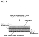
- a schematic sectional view showing the composite copper foil with carrier is shown in FIG. 1. When the cross-section is viewed, a nickel layer or a nickel alloy layer to be a metal layer for forming the resistor circuit is positioned in the location sandwiched between the copper carrier and the copper layer for forming the circuit.
- FIG. 1 shows the outer surface of the copper layer for forming the circuit that has undergone a nodular treatment, this nodular treatment is optional.
- the bonding strength of the copper foil circuits to an insulating material does not become an issue even if the nodular treatment is omitted.
- the nodular treatment is a treatment to deposit copper microparticles by burn plating of copper in the same manner as normally conducted to the bonding surface of copper foil, and to fix these copper microparticles by level plating of copper to prevent the separation of these copper microparticles. Since the copper carrier is made of the same material as the copper foil layer for forming the circuit, such a structure can minimize the dimensional change of the substrate after removing the carrier.
- the nickel layer or the nickel alloy layer to be a metal layer for forming the resistor circuit is formed on the flat surface of the copper foil, a fine resistor circuit can be formed, the degree of freedom for the design of the resistor circuit increases, and the stability of the resistance values is improved.
- a so called copper foil is used as the copper carrier and it may be formed of either an electrodeposited copper foil or a rolled copper foil.
- the composite copper foil with carrier according to claim 1 can use the copper foil layer itself for the carrier as the conductor. Therefore, when the metal layer for forming the resistor circuit and the copper foil layer for forming the circuit is manufactured by the electrodepositing method, the copper carrier can be used as the base material for electrodepositing the nickel layer or the nickel alloy layer to be a metal layer for forming the resistor circuit and the copper foil layer for forming the circuit on the surface of the copper carrier, by cathode-polarizing the copper carrier in a prescribed solution.
- the copper carrier can be used as an electrode to impress a voltage to the facing electrode, and nickel for forming the metal layer for forming the resistor circuit, and copper for forming the copper foil layer for forming the circuit can be deposited efficiently on the surface of the copper carrier.
- rust prevention treatment is generally performed for preventing oxidation during hot pressing for manufacturing a copper clad laminate, using an inorganic element such as zinc or a zinc alloy, or an organic agent such as benzotriazole or imidazole to secure the storage stability of the composite copper foil with carrier for a long period of time.
- an inorganic element such as zinc or a zinc alloy, or an organic agent such as benzotriazole or imidazole to secure the storage stability of the composite copper foil with carrier for a long period of time.
- the same rust prevention treatment is performed on the surface after the nodular treatment.
- such a rust prevention layer is an extremely thin film, it is omitted from the description of the composite copper foil with carrier according to claim 1.
- the composite copper foil with carrier according to claim 1 is used for manufacturing a printed wiring board with resistor circuits using the etching method that will be described later. Therefore, the thickness of the nickel layer or the nickel alloy layer to be a metal layer for forming the resistor circuit provided between the copper carrier and the copper foil layer for forming the circuit is adequately determined in consideration of the manufacturing method.
- the composite copper foil with carrier according to claim 1 may be of a peelable type from which the carrier can be released. In such a case, a metal layer, an organic layer, or another inorganic layer may be provided as an interface layer between the copper carrier and the metal layer for forming the resistor circuit.
- the thickness of said nickel layer or nickel alloy layer to be the metal layer for forming the resistor circuit in the composite copper foil with a carrier according to claim 1 is 0.01 ⁇ m to 4 ⁇ m.
- the electrochemically deposited nickel layer or nickel alloy layer is known to excel in deposition stability, and to form a uniform film with very little deposition defect in comparison with other metals. Particularly according to electroless plating, more stable deposition can be achieved when a nickel layer or a nickel alloy layer is formed. Therefore, it is practically possible to form a metal layer for forming a resistor circuit having a thickness thinner than 0.01 ⁇ m. In order to secure the mechanical strength of the nickel resistor circuits that is sufficient for practical use, it is considered that a thickness of at least about 1 ⁇ m is required.
- the present inventors considered to make the nickel layer or nickel alloy layer as thin as possible, and decided the value of 0.01 ⁇ m as the limit to be able to form a thin film without defects, and to recognize as a thickness.
- the use of a physical procedure such as vapor deposition and sputtering is also useful.
- the thickness of the metal layer for forming the resistor circuit thinner than 1 ⁇ m is confirmed, it is preferable to measure the thickness as a calculated thickness by dissolving only the metal layer for forming the resistor circuit, in addition to the procedure such as the use of the film thickness gauge.
- the reason why the upper limit is decided to 4 ⁇ m is as follows: The larger the thickness of the metal layer for the resistor circuit, the smaller the electrical resistance determined by the cross-sectional area of the resistor circuit. Therefore, the thickness of the metal layer for forming the resistor circuit should primarily be determined optionally by the design resistance. However, since the composite copper foil with carrier according to the present invention is used for manufacturing a printed wiring board with resistor circuits using the etching method that will be described later, the copper foil must have an adequate thickness that can form a preferable resistor circuit by etching. If the thickness of the metal layer for the resistor circuit becomes excessive at this time, the etching factor of the metal layer for the resistor circuit will be deteriorated.
- the thickness of the metal layer for the resistor circuit exceeds 4 ⁇ m, the etching factor becomes deteriorated, the linearity of the edge of the resistor circuit is rapidly deteriorated, and the stability of the profile of the resistor circuit starts to be lost.
- the nickel alloy layer to be the metal layer for forming the resistor circuit in the composite copper foil with a carrier according to claim 1 or 2 is made of a nickel-based alloy that contains at least one selected from a group consisting of phosphorus, boron, sulfur, titanium, vanadium, chromium, manganese, iron, cobalt, zinc, molybdenum, tungsten, tin, antimony, and copper.
- the purpose of using the nickel-based alloy layer is that a higher resistance value is expected in comparison with the metal layer for forming the resistor circuit that used nickel alone. Therefore, if the nickel-based alloy layer has the same thickness and the same circuit width as the nickel layer, the nickel-based alloy layer has a higher resistance value, and can be designed as a thicker circuit. Such a thick circuit is difficult to cause breaking of wiring in comparison with a thin circuit.
- the nickel-based alloy is an alloy based on nickel and contains at least one of other alloy elements.
- the alloy elements used here are selected from a group consisting of phosphorus, boron, sulfur, titanium, vanadium, chromium, manganese, iron, cobalt, zinc, molybdenum, tungsten, tin, antimony, and copper. These alloy elements can be used alone, or in combination of two or more. In particular, the addition of 10% by weight or more phosphorus in nickel is preferable, because the nickel becomes amorphous, and shows a very high resistance value. The addition of a trace of antimony also significantly increases the resistance value of nickel. There is no limit in the quantities of these alloy elements, and the composition that can achieve the desired resistance value may be selected in consideration of the design of the resistor circuit.
- the invention of claim 4 is a method for manufacturing a printed wiring board with resistor circuits comprising copper foil circuits and resistor circuits using a composite copper foil with a carrier comprising a nickel layer or a nickel alloy layer for forming a resistor circuit according to any of claims 1 through 3, comprising the steps of forming a copper etching resist layer on the surface of said copper foil for forming the circuit of the composite copper foil with a carrier, and exposing and developing the circuit pattern of the copper foil circuits to be formed on said copper etching resist layer; forming the copper foil circuits by etching the copper foil for forming the circuit using a copper etching solution that does not dissolve the nickel layer or the nickel alloy layer; removing the copper etching resist layer; fabricating a copper clad laminate by laminating the composite copper foil with a carrier on the material for composing an insulating layer in the state where the surface of the composite copper foil with a carrier on which the copper foil circuits are formed contacts the insulating layer composing material; removing the copper carrier
- FIGS. 2 to 7 This manufacturing method will be described in order below referring to FIGS. 2 to 7.
- the manufacturing method begin with the state of a composite copper foil with carrier, and a copper etching resist layer is formed on the surface that has undergone the nodular treatment of the copper foil for forming the circuit.
- the etching resist layer can be formed using a dry film, a liquid resist, or the like, but the materials are not limited to the above.
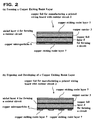
- FIG. 2 (a) shows the above-described step.
- a circuit pattern to be copper foil circuits formed on the copper etching resist layer is exposed and developed as shown in FIG. 2 (b).
- the copper foil layer for forming the circuit is etched with a copper etching solution that does not dissolve the nickel layer or the nickel alloy layer, to form copper foil circuits on the surface of the copper foil layer for forming the resistor circuit.
- the "copper etching solution that does not dissolve the nickel layer or the nickel alloy layer” used here means an alkaline etching solution for copper. Such an etching solution can etch copper without damaging the nickel layer or the nickel alloy layer.
- the schematic sectional view of the composite copper foil with carrier after forming the copper foil circuits is shown in FIG. 3 (c). After the formation of the copper foil circuits have been completed, the copper etching resist layer is released.
- the releasing solution used here is a commonly used alkaline resist releasing solution.
- FIG. 3 (d) shows the state after the copper etching resist layer has been released.
- a copper clad laminate is manufactured.
- an insulating layer composing material for composing a resin base e.g., prepreg
- hot pressing for manufacturing the copper clad laminate is performed in the state shown in FIG. 4 (e), so that the surface of the composite copper foil with carrier on which the copper foil circuits have been formed contacts the insulating layer composing material.
- the composite copper foil with carrier using two prepreg sheets after forming copper foil circuits is shown on its respective outsides as an example. Therefore, a single-face board or a multi-layer board having three or more layers may be manufactured without any problems.
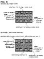
- the copper carrier to be positioned on the outer layer of the copper clad laminate must be removed to expose the metal layer for forming the resistor circuit. It is important at this time to use an alkaline etching solution for copper using ammonium persulfate or the like, or a mixed solution of sulfuric acid and hydrogen peroxide as the copper etching solution for removing the copper foil used for the carrier, in order to prevent the dissolution of the nickel layer or the nickel alloy layer as the metal layer for forming the resistor circuit, and to etch only copper. This is because if the thickness of the metal layer for forming the resistor circuit is varied, the resistance cannot be controlled accurately. While in the case where the above-described peelable type composite copper foil with carrier is used, the carrier can be removed by releasing. FIG. 5 (f) shows the state after the copper foil for the carrier has been removed.
- FIG. 5 (g) shows the state after the nickel etching resist layer has been formed.
- the nickel etching resist layer at this time is not necessarily a special etching resist layer.
- the same etching resist layer as the above-described copper etching resist layer can be used.
- the resistor circuit pattern of the nickel resistor circuits is exposed and developed.
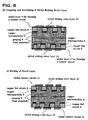
- the state after developing is shown in FIG 6 (h).
- the resistor circuit is formed by etching. At this time, it is preferable to use a selective nickel etching solution that does not dissolve copper.
- FIG. 6 (i) The state after the resistor circuit has been formed by etching is shown in FIG. 6 (i).
- FIG. 7 (j) shows, the nickel etching resist layer is removed to form the printed wiring board with resistor circuits according to the present invention.
- the term the selective nickel etching solution used herein is a solution to dissolve only nickel or nickel alloys without dissolving copper. The use of such a solution enables the resistor circuit to be manufactured at a high accuracy without damaging the copper circuit.
- the selective nickel etching solution is preferably any of (i) a sulfuric acid solution between 550 mL/L and 650 mL/L, (ii) a mixed solution of sulfuric acid and nitric acid, or (iii) a mixed solution of sulfuric acid and m-nitrobenzene sulfuric acid as described in claim 5.
- the first solution more preferably the concentration between 580 mL/L and 620 mL/L, is used for cathode-polarizing the copper clad laminate in the solution, and etching out the nickel layer or the nickel alloy layer by electrolysis.
- concentration decided between 550 mL/L and 650 mL/L is that if the concentration is lower than 550 mL/L, the etching speed is too low for the practical operation; and if the concentration exceeds 650 mL/L, the etching speed does not increase, and the rate of dissolving reaction decreases.
- the more preferable range, between 580 mL/L and 620 mL/L is the best range for the etching speed and the stability of the solution quality.
- concentrations there is no limitation in concentrations, and the optimal conditions can be established considering the process.
- the composite copper foil with carrier 2 used in this embodiment uses a electrodeposited copper foil having a thickness of 18 ⁇ m as a copper carrier 3.
- a nickel layer 4 for forming the resistor circuit having a thickness of 3 ⁇ m is formed on the shiny side of the copper carrier 3 using a so called treater of the copper foil, a copper foil layer 5 for forming the circuit is formed on the nickel layer 4 for forming the resistor circuit, copper microparticles 6 are further deposited, and both surfaces are subjected to the zinc rust prevention treatment.
- the zinc rust prevention layer is not shown.
- FIG. 2 (a) shows, a copper etching resist layer 7 is formed on the surface of the copper foil layer 5 for forming the circuit on which copper microparticles 6 are deposited.
- a dry film from Nichigo Alpho Co. Ltd. was used for forming the copper etching resist layer 7.
- FIG. 2 (b) shows, a circuit pattern for forming copper foil circuits 8 formed on the copper etching resist layer 7 was exposed and developed.
- FIGS. 2 (a) and 2 (b) show, a copper etching resist layer 7 is also formed on the entire surface of the copper carrier 3 using the same dry film.
- FIG. 3 (c) shows a schematic sectional view of the composite copper foil with carrier 2 after the copper foil circuits 8 have been formed.
- the copper etching resist layer 7 is released.
- the releasing solution used herein was a commercially available alkaline resist releasing solution.
- the state after the removal of the copper etching resist layer 7 has been completed is shown in FIG. 3 (d).
- a copper clad laminate 10 is manufactured by hot-pressing the composite copper foil with carrier 2 on which the copper foil circuits 8 are formed, and prepreg 9 composing the resin base.
- FIG. 4 (e) shows, 2 sheets of prepreg 9 were used, and a composite copper foil with carrier after copper foil circuits 8 had been formed was disposed on each outer side of the prepreg 9 to form a double-sided board.
- the term prepreg is generally used to express the state before curing, and the term base material or insulating base material is used to express the state after curing, the term prepreg is used either before curing or after curing for the ease of explanation in this embodiment.
- FIG. 5 (f) shows the state after the copper foil layer 3 for the carrier has been removed.
- a nickel etching resist layer 12 is formed on the nickel layer 4 for forming the resistor circuit 11.
- the state after the nickel etching resist layer 12 has been formed is shown in FIG. 5 (g).
- the same etching resist layer as the above-described copper etching resist layer 7 was used as the nickel etching resist layer 12.
- FIG. 6 (h) shows the state after developing.
- the nickel resistor circuits 11 were removed by etching using a selective nickel etching solution.
- a sulfuric acid solution prepared by adding 600 mL of special-grade sulfuric acid in 1 L of ion-exchanged water, and the structure as shown in FIG. 6 (i) was obtained.
- the nickel etching resist layer 12 was removed as shown in FIG. 7 (j) using a commercially available etching resist releasing solution to form the printed wiring board with resistor circuits 1.
- the printed wiring board with resistor circuits 1 thus obtained had an excellent stability of circuit width as the circuit accuracy, and the accuracy of the completed resistor circuits was satisfactory.
- the present inventors improved the linearity of the edges of the with laser processing to finish the printed wiring board with resistor circuits 1.
Landscapes
- Engineering & Computer Science (AREA)
- Microelectronics & Electronic Packaging (AREA)
- Manufacturing & Machinery (AREA)
- Parts Printed On Printed Circuit Boards (AREA)
- Manufacturing Of Printed Circuit Boards (AREA)
Abstract
There are provided an electrodeposited copper foil with
carrier that can be used for manufacturing a printed wiring
board that excels in the finished accuracy of the resistor
circuit in comparison with a conventional printed wiring
board with resistor circuits, and a method for manufacturing
such a printed wiring board with resistor circuits.
The method for manufacturing a printed wiring board with
resistor circuits comprises the steps of previously forming
copper foil circuits using a copper foil for a printed wiring
board with resistor circuits comprising a nickel layer for
forming a resistor circuit between a copper carrier and a
copper foil layer for forming the circuit, whose surface layer
is subjected to a nodular treatment, using a copper etching
solution that does not etch the nickel layer; fabricating a
copper clad laminate using the copper foil after forming the
copper circuits, and a prepreg composing a resin base
material; removing the copper carrier to expose the nickel
layer for forming the resistor circuit, and etching the
resistor circuits to form the nickel resistor-circuits.
Description
- The present invention relates to a method for manufacturing a copper foil for forming a resistor circuit used in the manufacture of a printed wiring board with nickel resistor circuits, and a printed wiring board comprising such a resistor circuit; and to a printed wiring board comprising such a resistor circuit.
- Such a printed wiring board with resistor circuits is used in electric and electronic equipment that requires resistance control. Particularly with a rapid increase in the clock frequencies of computers in recent years, a resistor circuit of considerably high accuracy has been demanded increasingly on a circuit substrate.
- It has been pointed out that the thickness of the nickel layer forming the resistor circuit should be uniform, and the width of the resistor circuit should be uniformly controlled in order to improve the accuracy of the finished resistor circuit, and is a matter of course in considering the electrical resistance of metals.
- A conventional printed wiring board with resistor circuits has been manufactured by forming a nickel layer for forming the resistor circuit on a surface of a base material used for bonding a copper that has undergone a nodular treatment (a treatment for depositing fine copper grains to obtain the anchoring effect), forming copper foil circuits on the copper foil side or forming a resistor circuit on a nickel layer for forming the resistor circuit, and bonding the nickel layer to the base material.
- Alternatively, there has generally been adopted a method for manufacturing a printed wiring board with resistor circuits by forming copper foil circuits on a copper foil layer using an electrodeposited copper foil with carrier, bonding the copper foil circuits on a base material, removing the carrier, thereafter forming a nickel layer for forming the resistor circuit using a plating method, and forming nickel resistor circuits using an etching method.
- However, since the above-described method for manufacturing a printed wiring board with resistor circuits, by using a copper foil having a nickel layer for the resistor circuit formed on the nodulated surface side used for bonding the copper foil on the base material, is affected by the uneven nodulated surface, the thickness of the nickel layer easily become uneven, and a resistor circuit of high accuracy cannot been formed.
- Also when an electrodeposited copper foil with carrier is used, there has been a problem that the dimensional accuracy as a printed wiring board is deteriorated when the carrier consisting of a different metal such as aluminum is removed after copper foil circuits are formed in the state of an electrodeposited copper foil with carrier, and bonding the copper foil to the base material.
- The present inventors conducted repeated studies, and discovered a method for an electrodeposited copper foil with carrier that can be used for manufacturing a printed wiring board with resistor circuits having an excellent accuracy of the completed resistor circuit and an excellent dimensional stability of the completed printed wiring board; and a method for manufacturing such a printed wiring board with resistor circuits. The present invention will be described below.
- The invention according to
claim 1 is a composite copper foil with carrier for manufacturing a printed wiring board with resistor circuits comprising a metal layer for forming the resistor circuit between a copper carrier and a copper layer for forming the circuit. The metal layer for forming the resistor circuit is characterized to be a nickel layer or a nickel alloy layer. A schematic sectional view showing the composite copper foil with carrier is shown in FIG. 1. When the cross-section is viewed, a nickel layer or a nickel alloy layer to be a metal layer for forming the resistor circuit is positioned in the location sandwiched between the copper carrier and the copper layer for forming the circuit. Although FIG. 1 shows the outer surface of the copper layer for forming the circuit that has undergone a nodular treatment, this nodular treatment is optional. As is obvious from the following description of the manufacturing method, since the copper foil circuits formed of the copper layer for forming the circuit of the composite copper foil with carrier according to the present invention is embedded when processed into a printed wiring board, the bonding strength of the copper foil circuits to an insulating material does not become an issue even if the nodular treatment is omitted. The nodular treatment is a treatment to deposit copper microparticles by burn plating of copper in the same manner as normally conducted to the bonding surface of copper foil, and to fix these copper microparticles by level plating of copper to prevent the separation of these copper microparticles. Since the copper carrier is made of the same material as the copper foil layer for forming the circuit, such a structure can minimize the dimensional change of the substrate after removing the carrier. Furthermore, since the nickel layer or the nickel alloy layer to be a metal layer for forming the resistor circuit is formed on the flat surface of the copper foil, a fine resistor circuit can be formed, the degree of freedom for the design of the resistor circuit increases, and the stability of the resistance values is improved. - A so called copper foil is used as the copper carrier and it may be formed of either an electrodeposited copper foil or a rolled copper foil. The composite copper foil with carrier according to
claim 1 can use the copper foil layer itself for the carrier as the conductor. Therefore, when the metal layer for forming the resistor circuit and the copper foil layer for forming the circuit is manufactured by the electrodepositing method, the copper carrier can be used as the base material for electrodepositing the nickel layer or the nickel alloy layer to be a metal layer for forming the resistor circuit and the copper foil layer for forming the circuit on the surface of the copper carrier, by cathode-polarizing the copper carrier in a prescribed solution. Also, when the metal layer for forming the resistor circuit and the copper layer for forming the circuit are manufactured by sputtering or vapor deposition, the copper carrier can be used as an electrode to impress a voltage to the facing electrode, and nickel for forming the metal layer for forming the resistor circuit, and copper for forming the copper foil layer for forming the circuit can be deposited efficiently on the surface of the copper carrier. - Since the surfaces of the copper carrier and the copper foil layer for forming the circuit are normally exposed to the air, rust prevention treatment is generally performed for preventing oxidation during hot pressing for manufacturing a copper clad laminate, using an inorganic element such as zinc or a zinc alloy, or an organic agent such as benzotriazole or imidazole to secure the storage stability of the composite copper foil with carrier for a long period of time. When copper microparticles are formed and the nodular treatment is performed, the same rust prevention treatment is performed on the surface after the nodular treatment. However, since such a rust prevention layer is an extremely thin film, it is omitted from the description of the composite copper foil with carrier according to
claim 1. - The composite copper foil with carrier according to
claim 1 is used for manufacturing a printed wiring board with resistor circuits using the etching method that will be described later. Therefore, the thickness of the nickel layer or the nickel alloy layer to be a metal layer for forming the resistor circuit provided between the copper carrier and the copper foil layer for forming the circuit is adequately determined in consideration of the manufacturing method. However, the composite copper foil with carrier according toclaim 1 may be of a peelable type from which the carrier can be released. In such a case, a metal layer, an organic layer, or another inorganic layer may be provided as an interface layer between the copper carrier and the metal layer for forming the resistor circuit. - According
claim 2, the thickness of said nickel layer or nickel alloy layer to be the metal layer for forming the resistor circuit in the composite copper foil with a carrier according toclaim 1 is 0.01 µm to 4 µm. The electrochemically deposited nickel layer or nickel alloy layer is known to excel in deposition stability, and to form a uniform film with very little deposition defect in comparison with other metals. Particularly according to electroless plating, more stable deposition can be achieved when a nickel layer or a nickel alloy layer is formed. Therefore, it is practically possible to form a metal layer for forming a resistor circuit having a thickness thinner than 0.01 µm. In order to secure the mechanical strength of the nickel resistor circuits that is sufficient for practical use, it is considered that a thickness of at least about 1 µm is required. On the other hand, if a thinner nickel layer or nickel alloy layer can be formed, an excellent area resistance can be obtained even if the width of the resistor circuit is large. Therefore, the present inventors considered to make the nickel layer or nickel alloy layer as thin as possible, and decided the value of 0.01 µm as the limit to be able to form a thin film without defects, and to recognize as a thickness. In order to form a metal layer for forming a resistor circuit having a thickness thinner than 1 µm, the use of a physical procedure such as vapor deposition and sputtering is also useful. Also, when the thickness of the metal layer for forming the resistor circuit thinner than 1 µm is confirmed, it is preferable to measure the thickness as a calculated thickness by dissolving only the metal layer for forming the resistor circuit, in addition to the procedure such as the use of the film thickness gauge. - Whereas, the reason why the upper limit is decided to 4 µm is as follows: The larger the thickness of the metal layer for the resistor circuit, the smaller the electrical resistance determined by the cross-sectional area of the resistor circuit. Therefore, the thickness of the metal layer for forming the resistor circuit should primarily be determined optionally by the design resistance. However, since the composite copper foil with carrier according to the present invention is used for manufacturing a printed wiring board with resistor circuits using the etching method that will be described later, the copper foil must have an adequate thickness that can form a preferable resistor circuit by etching. If the thickness of the metal layer for the resistor circuit becomes excessive at this time, the etching factor of the metal layer for the resistor circuit will be deteriorated. That is, if the thickness of the metal layer for the resistor circuit exceeds 4 µm, the etching factor becomes deteriorated, the linearity of the edge of the resistor circuit is rapidly deteriorated, and the stability of the profile of the resistor circuit starts to be lost.
- According to
claim 3, the nickel alloy layer to be the metal layer for forming the resistor circuit in the composite copper foil with a carrier according toclaim - The purpose of using the nickel-based alloy layer is that a higher resistance value is expected in comparison with the metal layer for forming the resistor circuit that used nickel alone. Therefore, if the nickel-based alloy layer has the same thickness and the same circuit width as the nickel layer, the nickel-based alloy layer has a higher resistance value, and can be designed as a thicker circuit. Such a thick circuit is difficult to cause breaking of wiring in comparison with a thin circuit. The nickel-based alloy is an alloy based on nickel and contains at least one of other alloy elements.
- The alloy elements used here are selected from a group consisting of phosphorus, boron, sulfur, titanium, vanadium, chromium, manganese, iron, cobalt, zinc, molybdenum, tungsten, tin, antimony, and copper. These alloy elements can be used alone, or in combination of two or more. In particular, the addition of 10% by weight or more phosphorus in nickel is preferable, because the nickel becomes amorphous, and shows a very high resistance value. The addition of a trace of antimony also significantly increases the resistance value of nickel. There is no limit in the quantities of these alloy elements, and the composition that can achieve the desired resistance value may be selected in consideration of the design of the resistor circuit.
- The invention of
claim 4 is a method for manufacturing a printed wiring board with resistor circuits comprising copper foil circuits and resistor circuits using a composite copper foil with a carrier comprising a nickel layer or a nickel alloy layer for forming a resistor circuit according to any ofclaims 1 through 3, comprising the steps of forming a copper etching resist layer on the surface of said copper foil for forming the circuit of the composite copper foil with a carrier, and exposing and developing the circuit pattern of the copper foil circuits to be formed on said copper etching resist layer; forming the copper foil circuits by etching the copper foil for forming the circuit using a copper etching solution that does not dissolve the nickel layer or the nickel alloy layer; removing the copper etching resist layer; fabricating a copper clad laminate by laminating the composite copper foil with a carrier on the material for composing an insulating layer in the state where the surface of the composite copper foil with a carrier on which the copper foil circuits are formed contacts the insulating layer composing material; removing the copper carrier positioned on the outer layer of said copper clad laminate to expose the nickel layer or the nickel alloy layer for forming the resistor circuit; forming a nickel etching resist layer on said nickel layer or nickel alloy layer, and exposing and developing the resistor circuit pattern; forming the resistor circuit by resistor-circuit etching using a selective etching solution for nickel or nickel alloy; and removing the nickel etching resist layer. - This manufacturing method will be described in order below referring to FIGS. 2 to 7. The manufacturing method begin with the state of a composite copper foil with carrier, and a copper etching resist layer is formed on the surface that has undergone the nodular treatment of the copper foil for forming the circuit. The etching resist layer can be formed using a dry film, a liquid resist, or the like, but the materials are not limited to the above. FIG. 2 (a) shows the above-described step. Then, a circuit pattern to be copper foil circuits formed on the copper etching resist layer is exposed and developed as shown in FIG. 2 (b). At this time, it is preferable to form a copper etching resist layer or a backup film layer over the entire surface of the copper carrier as FIGS. 2 (a) and (b) show, so as not to be damaged by the etching solution.
- Thereafter, the copper foil layer for forming the circuit is etched with a copper etching solution that does not dissolve the nickel layer or the nickel alloy layer, to form copper foil circuits on the surface of the copper foil layer for forming the resistor circuit. The "copper etching solution that does not dissolve the nickel layer or the nickel alloy layer" used here means an alkaline etching solution for copper. Such an etching solution can etch copper without damaging the nickel layer or the nickel alloy layer. The schematic sectional view of the composite copper foil with carrier after forming the copper foil circuits is shown in FIG. 3 (c). After the formation of the copper foil circuits have been completed, the copper etching resist layer is released. The releasing solution used here is a commonly used alkaline resist releasing solution. FIG. 3 (d) shows the state after the copper etching resist layer has been released.
- By hot-pressing the composite copper foil with carrier on which the copper foil circuits are formed and an insulating layer composing material for composing a resin base (e.g., prepreg), a copper clad laminate is manufactured. At this time, hot pressing for manufacturing the copper clad laminate is performed in the state shown in FIG. 4 (e), so that the surface of the composite copper foil with carrier on which the copper foil circuits have been formed contacts the insulating layer composing material. In FIG. 4 (e), the composite copper foil with carrier using two prepreg sheets after forming copper foil circuits is shown on its respective outsides as an example. Therefore, a single-face board or a multi-layer board having three or more layers may be manufactured without any problems.
- After the manufacture of the copper clad laminate has been completed, the copper carrier to be positioned on the outer layer of the copper clad laminate must be removed to expose the metal layer for forming the resistor circuit. It is important at this time to use an alkaline etching solution for copper using ammonium persulfate or the like, or a mixed solution of sulfuric acid and hydrogen peroxide as the copper etching solution for removing the copper foil used for the carrier, in order to prevent the dissolution of the nickel layer or the nickel alloy layer as the metal layer for forming the resistor circuit, and to etch only copper. This is because if the thickness of the metal layer for forming the resistor circuit is varied, the resistance cannot be controlled accurately. While in the case where the above-described peelable type composite copper foil with carrier is used, the carrier can be removed by releasing. FIG. 5 (f) shows the state after the copper foil for the carrier has been removed.
- Next, in order to form a resistor circuit, a nickel etching resist layer is formed on the nickel layer or the nickel alloy layer as the metal layer for forming the resistor circuit. FIG. 5 (g) shows the state after the nickel etching resist layer has been formed. The nickel etching resist layer at this time is not necessarily a special etching resist layer. The same etching resist layer as the above-described copper etching resist layer can be used.
- After the nickel etching resist layer has been formed, the resistor circuit pattern of the nickel resistor circuits is exposed and developed. The state after developing is shown in FIG 6 (h).
- After the development of the nickel etching resist layer has been completed, the resistor circuit is formed by etching. At this time, it is preferable to use a selective nickel etching solution that does not dissolve copper. The state after the resistor circuit has been formed by etching is shown in FIG. 6 (i). Finally, as FIG. 7 (j) shows, the nickel etching resist layer is removed to form the printed wiring board with resistor circuits according to the present invention.
- The term the selective nickel etching solution used herein is a solution to dissolve only nickel or nickel alloys without dissolving copper. The use of such a solution enables the resistor circuit to be manufactured at a high accuracy without damaging the copper circuit. The selective nickel etching solution is preferably any of (i) a sulfuric acid solution between 550 mL/L and 650 mL/L, (ii) a mixed solution of sulfuric acid and nitric acid, or (iii) a mixed solution of sulfuric acid and m-nitrobenzene sulfuric acid as described in
claim 5. - The first solution, more preferably the concentration between 580 mL/L and 620 mL/L, is used for cathode-polarizing the copper clad laminate in the solution, and etching out the nickel layer or the nickel alloy layer by electrolysis. The reason why the concentration is decided between 550 mL/L and 650 mL/L is that if the concentration is lower than 550 mL/L, the etching speed is too low for the practical operation; and if the concentration exceeds 650 mL/L, the etching speed does not increase, and the rate of dissolving reaction decreases. The more preferable range, between 580 mL/L and 620 mL/L, is the best range for the etching speed and the stability of the solution quality. For the second and third solutions, there is no limitation in concentrations, and the optimal conditions can be established considering the process.
-
- FIG. 1 is a schematic sectional view showing a composite copper foil with carrier; and
- FIGS. 2 through 7 are conceptual diagrams showing the flow of manufacturing a printed wiring board with resistor circuits.
-
- The present invention will be described below in further detail referring to an embodiment of a printed
wiring board 1 with resistor circuits according to the present invention. - This embodiment will be described referring to FIGS. 2 to 7. The composite copper foil with
carrier 2 used in this embodiment uses a electrodeposited copper foil having a thickness of 18 µm as acopper carrier 3. Anickel layer 4 for forming the resistor circuit having a thickness of 3 µm is formed on the shiny side of thecopper carrier 3 using a so called treater of the copper foil, acopper foil layer 5 for forming the circuit is formed on thenickel layer 4 for forming the resistor circuit,copper microparticles 6 are further deposited, and both surfaces are subjected to the zinc rust prevention treatment. Here, the zinc rust prevention layer is not shown. - Then, as FIG. 2 (a) shows, a copper etching resist
layer 7 is formed on the surface of thecopper foil layer 5 for forming the circuit on whichcopper microparticles 6 are deposited. For forming the copper etching resistlayer 7, a dry film from Nichigo Alpho Co. Ltd. was used. As FIG. 2 (b) shows, a circuit pattern for formingcopper foil circuits 8 formed on the copper etching resistlayer 7 was exposed and developed. At this time, as FIGS. 2 (a) and 2 (b) show, a copper etching resistlayer 7 is also formed on the entire surface of thecopper carrier 3 using the same dry film. - Thereafter,
copper foil circuits 8 were formed on the surface of the composite copper foil withcarrier 2 by etching thecopper foil layer 5 for forming the circuit from the surface on whichcopper microparticles 6 are deposited using an alkaline copper etching solution. FIG. 3 (c) shows a schematic sectional view of the composite copper foil withcarrier 2 after thecopper foil circuits 8 have been formed. - After the formation of the
copper foil circuits 8 has been completed, the copper etching resistlayer 7 is released. The releasing solution used herein was a commercially available alkaline resist releasing solution. The state after the removal of the copper etching resistlayer 7 has been completed is shown in FIG. 3 (d). - A copper clad
laminate 10 is manufactured by hot-pressing the composite copper foil withcarrier 2 on which thecopper foil circuits 8 are formed, andprepreg 9 composing the resin base. At this time, the surface of the composite copper foil withcarrier 2 on which thecopper foil circuits 8 was disposed so as to contact theprepreg 9, and these were laminated and compressed as shown in FIG. 4 (e). At this time, as FIG. 4 (e) shows, 2 sheets ofprepreg 9 were used, and a composite copper foil with carrier aftercopper foil circuits 8 had been formed was disposed on each outer side of theprepreg 9 to form a double-sided board. Although the term prepreg is generally used to express the state before curing, and the term base material or insulating base material is used to express the state after curing, the term prepreg is used either before curing or after curing for the ease of explanation in this embodiment. - After the manufacture of the copper clad
laminate 10 had been completed, thecopper foil carrier 3 positioned on the outer layer of the copper cladlaminate 10 was etched off to expose thenickel layer 4 for forming the resistor circuit. At this time, an ammonium persulfate solution was used as the copper etching solution so as to prevent the dissolution of thenickel layer 4 for forming the resistor circuit. FIG. 5 (f) shows the state after thecopper foil layer 3 for the carrier has been removed. - Next, a nickel etching resist
layer 12 is formed on thenickel layer 4 for forming theresistor circuit 11. The state after the nickel etching resistlayer 12 has been formed is shown in FIG. 5 (g). Here, the same etching resist layer as the above-described copper etching resistlayer 7 was used as the nickel etching resistlayer 12. - After the formation of the nickel etching resist
layer 12 had been completed, the resistor circuit pattern of thenickel resistor circuits 11 was exposed and developed. FIG. 6 (h) shows the state after developing. - After the development of the nickel etching resist
layer 12 had been completed, thenickel resistor circuits 11 were removed by etching using a selective nickel etching solution. As the selective nickel etching solution, a sulfuric acid solution prepared by adding 600 mL of special-grade sulfuric acid in 1 L of ion-exchanged water, and the structure as shown in FIG. 6 (i) was obtained. - Finally, the nickel etching resist
layer 12 was removed as shown in FIG. 7 (j) using a commercially available etching resist releasing solution to form the printed wiring board withresistor circuits 1. The printed wiring board withresistor circuits 1 thus obtained had an excellent stability of circuit width as the circuit accuracy, and the accuracy of the completed resistor circuits was satisfactory.
However, in order to make thenickel resistor circuits 11 on the completed printed wiring board withresistor circuits 1 more accurate, the present inventors improved the linearity of the edges of the with laser processing to finish the printed wiring board withresistor circuits 1. - The use of the composite copper foil with carrier according to the present invention, and the adoption of the above-described method for manufacturing a printed wiring board with resistor circuits have enabled a printed wiring board with resistor circuits that has the accuracy of completed circuits superior to conventional printed wiring boards to be manufactured. Therefore, the control of the resistor circuits becomes easy, and the applicable area of printed wiring boards with resistor circuits has been expanded dramatically.
Claims (6)
- A composite copper foil with a carrier for manufacturing a printed wiring board with resistor circuits, comprising a metal layer for forming the resistor circuit between a copper carrier and a copper foil layer for forming the circuit, whereinsaid metal layer for forming the resistor circuit is a nickel layer or a nickel alloy layer.
- The composite copper foil with a carrier according to claim 1, wherein the thickness of said nickel layer or nickel alloy layer to be the metal layer for forming the resistor circuit is 0.01 µm to 4 µm.
- The composite copper foil with a carrier according to claim 1 or 2, wherein said nickel alloy layer to be the metal layer for forming the resistor circuit, is a nickel-based alloy that contains at least one selected from a group consisting of phosphorus, boron, sulfur, titanium, vanadium, chromium, manganese, iron, cobalt, zinc, molybdenum, tungsten, tin, antimony, and copper.
- A method for manufacturing a printed wiring board with resistor circuits comprising copper foil circuits and resistor circuits, said method using a composite copper foil with a carrier comprising a nickel layer or a nickel alloy layer for forming a resistor circuit, said composite copper foil with a carrier being recited in any of claims 1 through 3, comprising the steps of.forming a copper etching resist layer on the surface of said copper foil for forming the circuit of the composite copper foil with a carrier, and exposing and developing the circuit pattern of the copper foil circuits to be formed on said copper etching resist layer,forming the copper foil circuits by etching the copper foil for forming the circuit using a copper etching solution that does not dissolve the nickel layer or the nickel alloy layer,removing the copper etching resist layer,fabricating a copper clad laminate by laminating and hot-pressing the composite copper foil with a carrier and the material for composing an insulating layer in the state where the surface of the composite copper foil with a carrier on which the copper foil circuits are formed contacts the insulating layer composing material,removing the copper carrier positioned on the outer layer of said copper clad laminate to expose the nickel layer or the nickel alloy layer for forming the resistor circuit,forming a nickel etching resist layer on said nickel layer or nickel alloy layer, and exposing and developing the resistor circuit pattern,forming the resistor circuit by resistor-circuit etching using an etching solution for nickel or nickel alloy, andremoving the nickel etching resist layer.
- The method for manufacturing a printed wiring board with resistor circuits according to claim 3, whereinsaid etching solution for nickel or nickel alloy is a selective etching solution that does not dissolve copper, selected from:(i) a sulfuric acid solution between 550 mL/L and 650 mL/L,(ii) a mixed solution of sulfuric acid and nitric acid, or(iii) a mixed solution of sulfuric acid and m-nitrobenzene sulfuric acid.
- A printed wiring board obtained by the method for manufacturing a printed wiring board with resistor circuits, said method being recited in claim 3 or 4.
Applications Claiming Priority (3)
| Application Number | Priority Date | Filing Date | Title |
|---|---|---|---|
| JP2000207016 | 2000-07-07 | ||
| JP2000207016 | 2000-07-07 | ||
| PCT/JP2001/005614 WO2002005604A1 (en) | 2000-07-07 | 2001-06-29 | Carrier-foiled composite copper foil, method for manufacturing printed circuit board with resistance circuit, and printed circuit board having resistance circuit |
Publications (1)
| Publication Number | Publication Date |
|---|---|
| EP1229768A1 true EP1229768A1 (en) | 2002-08-07 |
Family
ID=18703841
Family Applications (1)
| Application Number | Title | Priority Date | Filing Date |
|---|---|---|---|
| EP01945696A Withdrawn EP1229768A1 (en) | 2000-07-07 | 2001-06-29 | Carrier-foiled composite copper foil, method for manufacturing printed circuit board with resistance circuit, and printed circuit board having resistance circuit |
Country Status (6)
| Country | Link |
|---|---|
| US (1) | US6660406B2 (en) |
| EP (1) | EP1229768A1 (en) |
| KR (1) | KR100485765B1 (en) |
| CN (1) | CN1383706A (en) |
| TW (1) | TW507512B (en) |
| WO (1) | WO2002005604A1 (en) |
Families Citing this family (31)
| Publication number | Priority date | Publication date | Assignee | Title |
|---|---|---|---|---|
| JP3690962B2 (en) * | 2000-04-26 | 2005-08-31 | 三井金属鉱業株式会社 | Electrolytic copper foil with carrier foil, method for producing electrolytic copper foil with carrier foil, and copper-clad laminate |
| JP3396465B2 (en) * | 2000-08-25 | 2003-04-14 | 三井金属鉱業株式会社 | Copper clad laminate |
| US20030146191A1 (en) * | 2002-02-07 | 2003-08-07 | Ho-Ming Tong | Etching method for nickel-vanadium alloy |
| TW200420208A (en) * | 2002-10-31 | 2004-10-01 | Furukawa Circuit Foil | Ultra-thin copper foil with carrier, method of production of the same, and printed circuit board using ultra-thin copper foil with carrier |
| KR100468195B1 (en) * | 2002-11-28 | 2005-01-26 | 주식회사 호진플라텍 | A manufacturing process of multi-layer printed circuit board |
| JP4065215B2 (en) * | 2003-05-13 | 2008-03-19 | 福田金属箔粉工業株式会社 | Copper foil for printed wiring boards |
| US6872468B1 (en) * | 2003-10-09 | 2005-03-29 | Motorola, Inc. | Peelable circuit board foil |
| JP4713131B2 (en) * | 2004-11-19 | 2011-06-29 | 株式会社マルチ | Printed wiring board and method for manufacturing the printed wiring board |
| US7138068B2 (en) * | 2005-03-21 | 2006-11-21 | Motorola, Inc. | Printed circuit patterned embedded capacitance layer |
| US7241510B2 (en) * | 2005-05-27 | 2007-07-10 | Motorola, Inc. | Peelable circuit board foil |
| US7976956B2 (en) * | 2005-08-01 | 2011-07-12 | Furukawa Circuit Foil., Ltd. | Laminated circuit board |
| JP5052806B2 (en) * | 2006-03-29 | 2012-10-17 | 古河電気工業株式会社 | Conductive substrate with thin film resistive layer, method for producing conductive substrate with thin film resistive layer, and circuit board with thin film resistive layer |
| KR20090074834A (en) * | 2006-05-19 | 2009-07-08 | 대덕전자 주식회사 | Multilayer Copper Foil and Manufacturing Method of Printed Circuit Board Using the Same |
| TWM323107U (en) * | 2007-04-03 | 2007-12-01 | Jin-Chiuan Bai | Thin type semiconductor chip package substrate |
| KR100895820B1 (en) * | 2008-01-02 | 2009-05-06 | 주식회사 하이닉스반도체 | Circuit board for semiconductor package, manufacturing method thereof and semiconductor package having same |
| CN102104007B (en) * | 2009-12-21 | 2013-04-17 | 北大方正集团有限公司 | Method and equipment for manufacturing special circuit board |
| WO2013031913A1 (en) * | 2011-08-31 | 2013-03-07 | Jx日鉱日石金属株式会社 | Copper foil with carrier |
| TWI484073B (en) * | 2012-11-09 | 2015-05-11 | Jx日鑛日石金屬股份有限公司 | Surface treatment of copper foil and the use of its laminated board, copper laminated board, printed wiring board and electronic equipment |
| CN103009713A (en) * | 2012-11-28 | 2013-04-03 | 梅州市志浩电子科技有限公司 | Thermal compression bonding copper-clad plate by adopting polymethyl methacrylate as medium, printed circuit board as well as manufacturing method thereof |
| JP6190500B2 (en) * | 2015-08-06 | 2017-08-30 | Jx金属株式会社 | Copper foil with carrier, laminate, printed wiring board manufacturing method and electronic device manufacturing method |
| CN105163525A (en) * | 2015-08-19 | 2015-12-16 | 深圳市迅捷兴电路技术有限公司 | Method for fabricating inner-layer ultra-thick copper circuit board |
| CN106102352B (en) * | 2016-07-04 | 2019-10-15 | 广州兴森快捷电路科技有限公司 | A method of solving non-symmetrical line slab warping |
| JP2018122590A (en) * | 2017-02-02 | 2018-08-09 | Jx金属株式会社 | Metal foil with release layer, metal foil, laminate, printed wiring board, semiconductor package, electronic device, and method for manufacturing printed wiring board |
| US10057984B1 (en) * | 2017-02-02 | 2018-08-21 | Chang Chun Petrochemical Co., Ltd. | Composite thin copper foil and carrier |
| US11639557B2 (en) * | 2019-02-28 | 2023-05-02 | Circuit Foil Luxembourg | Composite copper foil and method of fabricating the same |
| CN111182735B (en) * | 2020-02-26 | 2024-01-26 | 东莞市天晖电子材料科技有限公司 | High-transmission single panel for LED lamp strip and preparation method thereof |
| CN114554684A (en) * | 2020-11-19 | 2022-05-27 | 广州方邦电子股份有限公司 | Composite metal foil and circuit board |
| CN113438830A (en) * | 2021-07-08 | 2021-09-24 | 江西柔顺科技有限公司 | Circuit board and preparation method thereof |
| CN113490344A (en) * | 2021-07-08 | 2021-10-08 | 江西柔顺科技有限公司 | Flexible circuit board and preparation method thereof |
| KR102950133B1 (en) * | 2021-09-30 | 2026-04-09 | 롯데에너지머티리얼즈 주식회사 | Ultra-thin Copper Foil With Carrier Foil For Easy Micro-hole Processing, Copper-clad Laminate Using The Same, And Manufacturing Methods Thereof |
| KR20250018027A (en) | 2023-07-28 | 2025-02-04 | 삼원동관 주식회사 | Apparatus and method of molding for branch type pipe |
Family Cites Families (13)
| Publication number | Priority date | Publication date | Assignee | Title |
|---|---|---|---|---|
| US3998601A (en) * | 1973-12-03 | 1976-12-21 | Yates Industries, Inc. | Thin foil |
| DE3321900C2 (en) * | 1982-06-16 | 1986-01-16 | Nitto Electric Industrial Co., Ltd., Ibaraki, Osaka | Substrate for a circuit with a resistive layer and method for its manufacture |
| JPS5916084A (en) * | 1982-07-19 | 1984-01-27 | Nitto Electric Ind Co Ltd | Input tablet |
| US4572768A (en) * | 1985-06-28 | 1986-02-25 | Square D Company | Treatment for copper foil |
| US5262247A (en) * | 1989-05-17 | 1993-11-16 | Fukuda Kinzoku Hakufun Kogyo Kabushiki Kaisha | Thin copper foil for printed wiring board |
| JPH0799378A (en) * | 1991-02-22 | 1995-04-11 | Planar Circuit Technol Inc | Method for forming resistor thin film layer on printed circuit board |
| JP3543348B2 (en) * | 1994-02-01 | 2004-07-14 | 日立化成工業株式会社 | Manufacturing method of multilayer wiring board |
| US6319620B1 (en) * | 1998-01-19 | 2001-11-20 | Mitsui Mining & Smelting Co., Ltd. | Making and using an ultra-thin copper foil |
| US5989727A (en) * | 1998-03-04 | 1999-11-23 | Circuit Foil U.S.A., Inc. | Electrolytic copper foil having a modified shiny side |
| JP4055026B2 (en) * | 1998-03-13 | 2008-03-05 | 日立化成工業株式会社 | Manufacturing method of build-up multilayer printed wiring board |
| JPH11354684A (en) * | 1998-06-09 | 1999-12-24 | Nitto Denko Corp | Low thermal expansion wiring board and multilayer wiring board |
| JP3142259B2 (en) * | 1998-11-30 | 2001-03-07 | 三井金属鉱業株式会社 | Copper foil for printed wiring board excellent in chemical resistance and heat resistance and method for producing the same |
| US6346335B1 (en) * | 2000-03-10 | 2002-02-12 | Olin Corporation | Copper foil composite including a release layer |
-
2001
- 2001-06-20 US US09/885,552 patent/US6660406B2/en not_active Expired - Lifetime
- 2001-06-27 TW TW090115588A patent/TW507512B/en not_active IP Right Cessation
- 2001-06-29 EP EP01945696A patent/EP1229768A1/en not_active Withdrawn
- 2001-06-29 CN CN01801916A patent/CN1383706A/en active Pending
- 2001-06-29 WO PCT/JP2001/005614 patent/WO2002005604A1/en not_active Ceased
- 2001-06-29 KR KR10-2002-7002591A patent/KR100485765B1/en not_active Expired - Fee Related
Non-Patent Citations (1)
| Title |
|---|
| See references of WO0205604A1 * |
Also Published As
| Publication number | Publication date |
|---|---|
| US20020004123A1 (en) | 2002-01-10 |
| KR20020042658A (en) | 2002-06-05 |
| KR100485765B1 (en) | 2005-04-28 |
| US6660406B2 (en) | 2003-12-09 |
| WO2002005604A1 (en) | 2002-01-17 |
| CN1383706A (en) | 2002-12-04 |
| TW507512B (en) | 2002-10-21 |
Similar Documents
| Publication | Publication Date | Title |
|---|---|---|
| US6660406B2 (en) | Method for manufacturing printed wiring board comprising electrodeposited copper foil with carrier and resistor circuit; and printed wiring board comprising resistor circuit | |
| US7790269B2 (en) | Ultra-thin copper foil with carrier and printed wiring board using ultra-thin copper foil with carrier | |
| EP1893006B1 (en) | Printed wiring board and method for producing the same | |
| KR100902970B1 (en) | Printed wiring board and circuit device using the same | |
| US5243320A (en) | Resistive metal layers and method for making same | |
| JP4087369B2 (en) | Ultra-thin copper foil with carrier and printed wiring board | |
| CN102301838B (en) | The rolled copper foil of electronic circuit or electrolytic copper foil and use their to form the method for electronic circuit | |
| US4889584A (en) | Method of producing conductor circuit boards | |
| CN104080951B (en) | Copper foil for printed wiring boards, laminates using the same, printed wiring boards, and electronic components | |
| JP4959052B2 (en) | Improved method of forming conductive traces and printed circuit manufactured thereby | |
| JP2004169181A (en) | Ultra-thin copper foil with carrier, method for producing the same, printed wiring board using ultra-thin copper foil with carrier | |
| JP2016168687A (en) | Composite metal foil and production method of the same, as well as printed wiring board | |
| TW201544636A (en) | Copper foil having carrier, manufacturing method for producing the copper foil having carrier, copper clad laminate and printed wiring board using the copper foil having carrier | |
| CN102265712B (en) | Method for forming electronic circuit | |
| EP1513382A2 (en) | Conductive sheet having conductive layer with improved adhesion and product including the same | |
| JP2001246691A (en) | Metal foil with carrier foil and method for producing the same | |
| JP2004263300A (en) | Copper foil for fine pattern printed wiring and manufacturing method thereof | |
| TWI853007B (en) | Metal foil for printed wiring board, carrier metal foil and metal-clad laminate, and method for producing printed wiring board using the same | |
| JP3906347B2 (en) | Copper foil for printed circuit | |
| EP1011111A1 (en) | Resistive metal layers and method for making same | |
| JP4257632B2 (en) | Copper foil with resistance layer and manufacturing method thereof | |
| JP2003200523A (en) | Resistance layer built-in copper clad laminated sheet and printed circuit board using the same | |
| JP2005307270A (en) | Electrolytic copper foil with carrier foil and method for producing electrolytic copper foil with carrier foil | |
| JP2003200524A (en) | Resistance layer built-in copper clad laminated sheet and printed circuit board using the same | |
| JP2014139337A (en) | Copper foil with carrier |
Legal Events
| Date | Code | Title | Description |
|---|---|---|---|
| PUAI | Public reference made under article 153(3) epc to a published international application that has entered the european phase |
Free format text: ORIGINAL CODE: 0009012 |
|
| 17P | Request for examination filed |
Effective date: 20020318 |
|
| AK | Designated contracting states |
Kind code of ref document: A1 Designated state(s): AT BE CH CY DE DK ES FI FR GB GR IE IT LI LU MC NL PT SE |
|
| STAA | Information on the status of an ep patent application or granted ep patent |
Free format text: STATUS: THE APPLICATION HAS BEEN WITHDRAWN |
|
| 18W | Application withdrawn |
Effective date: 20040428 |