EP1226947B1 - Dünnfilmbeschichtung eines geschlitzen Substrates und Verfahren zur Herstellung von geschlitzten Substraten - Google Patents
Dünnfilmbeschichtung eines geschlitzen Substrates und Verfahren zur Herstellung von geschlitzten Substraten Download PDFInfo
- Publication number
- EP1226947B1 EP1226947B1 EP02250377A EP02250377A EP1226947B1 EP 1226947 B1 EP1226947 B1 EP 1226947B1 EP 02250377 A EP02250377 A EP 02250377A EP 02250377 A EP02250377 A EP 02250377A EP 1226947 B1 EP1226947 B1 EP 1226947B1
- Authority
- EP
- European Patent Office
- Prior art keywords
- substrate
- layer
- thin film
- slot
- slotted
- Prior art date
- Legal status (The legal status is an assumption and is not a legal conclusion. Google has not performed a legal analysis and makes no representation as to the accuracy of the status listed.)
- Expired - Lifetime
Links
- 239000000758 substrate Substances 0.000 title claims description 93
- 239000010409 thin film Substances 0.000 title claims description 41
- 238000000034 method Methods 0.000 title claims description 37
- 238000009501 film coating Methods 0.000 title description 3
- 239000000463 material Substances 0.000 claims description 33
- 239000010408 film Substances 0.000 claims description 6
- 229910052751 metal Inorganic materials 0.000 claims description 6
- 239000002184 metal Substances 0.000 claims description 6
- 238000005488 sandblasting Methods 0.000 claims description 6
- 230000006835 compression Effects 0.000 claims description 3
- 238000007906 compression Methods 0.000 claims description 3
- 238000000151 deposition Methods 0.000 claims description 3
- 229920006254 polymer film Polymers 0.000 claims description 2
- 239000010410 layer Substances 0.000 description 127
- 230000004888 barrier function Effects 0.000 description 30
- VYPSYNLAJGMNEJ-UHFFFAOYSA-N Silicium dioxide Chemical compound O=[Si]=O VYPSYNLAJGMNEJ-UHFFFAOYSA-N 0.000 description 16
- 238000002161 passivation Methods 0.000 description 15
- XUIMIQQOPSSXEZ-UHFFFAOYSA-N Silicon Chemical compound [Si] XUIMIQQOPSSXEZ-UHFFFAOYSA-N 0.000 description 13
- 238000010304 firing Methods 0.000 description 13
- 239000012530 fluid Substances 0.000 description 13
- 229910052710 silicon Inorganic materials 0.000 description 13
- 239000010703 silicon Substances 0.000 description 13
- 230000008569 process Effects 0.000 description 10
- 229910052715 tantalum Inorganic materials 0.000 description 10
- GUVRBAGPIYLISA-UHFFFAOYSA-N tantalum atom Chemical compound [Ta] GUVRBAGPIYLISA-UHFFFAOYSA-N 0.000 description 10
- 229920000642 polymer Polymers 0.000 description 9
- 230000015572 biosynthetic process Effects 0.000 description 8
- 229920002120 photoresistant polymer Polymers 0.000 description 8
- 239000004020 conductor Substances 0.000 description 7
- 239000010931 gold Substances 0.000 description 7
- 229910052581 Si3N4 Inorganic materials 0.000 description 6
- 239000011521 glass Substances 0.000 description 6
- PCHJSUWPFVWCPO-UHFFFAOYSA-N gold Chemical compound [Au] PCHJSUWPFVWCPO-UHFFFAOYSA-N 0.000 description 6
- 229910052737 gold Inorganic materials 0.000 description 6
- 239000002245 particle Substances 0.000 description 6
- 239000004576 sand Substances 0.000 description 6
- HBMJWWWQQXIZIP-UHFFFAOYSA-N silicon carbide Chemical compound [Si+]#[C-] HBMJWWWQQXIZIP-UHFFFAOYSA-N 0.000 description 6
- 229910010271 silicon carbide Inorganic materials 0.000 description 6
- HQVNEWCFYHHQES-UHFFFAOYSA-N silicon nitride Chemical compound N12[Si]34N5[Si]62N3[Si]51N64 HQVNEWCFYHHQES-UHFFFAOYSA-N 0.000 description 6
- 238000004544 sputter deposition Methods 0.000 description 6
- 229910052782 aluminium Inorganic materials 0.000 description 5
- XAGFODPZIPBFFR-UHFFFAOYSA-N aluminium Chemical compound [Al] XAGFODPZIPBFFR-UHFFFAOYSA-N 0.000 description 5
- 238000005530 etching Methods 0.000 description 5
- 238000000623 plasma-assisted chemical vapour deposition Methods 0.000 description 5
- 239000004033 plastic Substances 0.000 description 5
- 229920003023 plastic Polymers 0.000 description 5
- 229960001866 silicon dioxide Drugs 0.000 description 5
- 235000012239 silicon dioxide Nutrition 0.000 description 5
- 239000000377 silicon dioxide Substances 0.000 description 5
- RVSGESPTHDDNTH-UHFFFAOYSA-N alumane;tantalum Chemical compound [AlH3].[Ta] RVSGESPTHDDNTH-UHFFFAOYSA-N 0.000 description 4
- 239000002131 composite material Substances 0.000 description 4
- 238000005553 drilling Methods 0.000 description 4
- 230000008020 evaporation Effects 0.000 description 4
- 238000001704 evaporation Methods 0.000 description 4
- 238000004519 manufacturing process Methods 0.000 description 4
- TWNQGVIAIRXVLR-UHFFFAOYSA-N oxo(oxoalumanyloxy)alumane Chemical compound O=[Al]O[Al]=O TWNQGVIAIRXVLR-UHFFFAOYSA-N 0.000 description 4
- 239000004065 semiconductor Substances 0.000 description 4
- 235000012431 wafers Nutrition 0.000 description 4
- 238000005520 cutting process Methods 0.000 description 3
- 239000007789 gas Substances 0.000 description 3
- 238000010438 heat treatment Methods 0.000 description 3
- 238000007747 plating Methods 0.000 description 3
- IJGRMHOSHXDMSA-UHFFFAOYSA-N Atomic nitrogen Chemical compound N#N IJGRMHOSHXDMSA-UHFFFAOYSA-N 0.000 description 2
- RYGMFSIKBFXOCR-UHFFFAOYSA-N Copper Chemical compound [Cu] RYGMFSIKBFXOCR-UHFFFAOYSA-N 0.000 description 2
- 239000004642 Polyimide Substances 0.000 description 2
- 239000011153 ceramic matrix composite Substances 0.000 description 2
- 239000011248 coating agent Substances 0.000 description 2
- 239000011247 coating layer Substances 0.000 description 2
- 238000000576 coating method Methods 0.000 description 2
- 229910052802 copper Inorganic materials 0.000 description 2
- 239000010949 copper Substances 0.000 description 2
- 230000007423 decrease Effects 0.000 description 2
- 230000003247 decreasing effect Effects 0.000 description 2
- 239000003989 dielectric material Substances 0.000 description 2
- 238000007373 indentation Methods 0.000 description 2
- 239000011156 metal matrix composite Substances 0.000 description 2
- 229920001721 polyimide Polymers 0.000 description 2
- 239000000843 powder Substances 0.000 description 2
- 230000005855 radiation Effects 0.000 description 2
- 230000009467 reduction Effects 0.000 description 2
- 241000894007 species Species 0.000 description 2
- OKTJSMMVPCPJKN-UHFFFAOYSA-N Carbon Chemical compound [C] OKTJSMMVPCPJKN-UHFFFAOYSA-N 0.000 description 1
- 239000004593 Epoxy Substances 0.000 description 1
- PIICEJLVQHRZGT-UHFFFAOYSA-N Ethylenediamine Chemical compound NCCN PIICEJLVQHRZGT-UHFFFAOYSA-N 0.000 description 1
- -1 FOX) Substances 0.000 description 1
- YCKRFDGAMUMZLT-UHFFFAOYSA-N Fluorine atom Chemical compound [F] YCKRFDGAMUMZLT-UHFFFAOYSA-N 0.000 description 1
- 240000007049 Juglans regia Species 0.000 description 1
- 235000009496 Juglans regia Nutrition 0.000 description 1
- 229910018487 Ni—Cr Inorganic materials 0.000 description 1
- UIIMBOGNXHQVGW-DEQYMQKBSA-M Sodium bicarbonate-14C Chemical compound [Na+].O[14C]([O-])=O UIIMBOGNXHQVGW-DEQYMQKBSA-M 0.000 description 1
- 229910004490 TaAl Inorganic materials 0.000 description 1
- NRTOMJZYCJJWKI-UHFFFAOYSA-N Titanium nitride Chemical compound [Ti]#N NRTOMJZYCJJWKI-UHFFFAOYSA-N 0.000 description 1
- 230000009471 action Effects 0.000 description 1
- 239000000853 adhesive Substances 0.000 description 1
- 230000001070 adhesive effect Effects 0.000 description 1
- 230000002411 adverse Effects 0.000 description 1
- QVGXLLKOCUKJST-UHFFFAOYSA-N atomic oxygen Chemical compound [O] QVGXLLKOCUKJST-UHFFFAOYSA-N 0.000 description 1
- 239000011324 bead Substances 0.000 description 1
- 238000005422 blasting Methods 0.000 description 1
- 239000000872 buffer Substances 0.000 description 1
- 229910052799 carbon Inorganic materials 0.000 description 1
- BGTFCAQCKWKTRL-YDEUACAXSA-N chembl1095986 Chemical compound C1[C@@H](N)[C@@H](O)[C@H](C)O[C@H]1O[C@@H]([C@H]1C(N[C@H](C2=CC(O)=CC(O[C@@H]3[C@H]([C@@H](O)[C@H](O)[C@@H](CO)O3)O)=C2C=2C(O)=CC=C(C=2)[C@@H](NC(=O)[C@@H]2NC(=O)[C@@H]3C=4C=C(C(=C(O)C=4)C)OC=4C(O)=CC=C(C=4)[C@@H](N)C(=O)N[C@@H](C(=O)N3)[C@H](O)C=3C=CC(O4)=CC=3)C(=O)N1)C(O)=O)=O)C(C=C1)=CC=C1OC1=C(O[C@@H]3[C@H]([C@H](O)[C@@H](O)[C@H](CO[C@@H]5[C@H]([C@@H](O)[C@H](O)[C@@H](C)O5)O)O3)O[C@@H]3[C@H]([C@@H](O)[C@H](O)[C@@H](CO)O3)O[C@@H]3[C@H]([C@H](O)[C@@H](CO)O3)O)C4=CC2=C1 BGTFCAQCKWKTRL-YDEUACAXSA-N 0.000 description 1
- 238000003486 chemical etching Methods 0.000 description 1
- 238000006243 chemical reaction Methods 0.000 description 1
- VNNRSPGTAMTISX-UHFFFAOYSA-N chromium nickel Chemical compound [Cr].[Ni] VNNRSPGTAMTISX-UHFFFAOYSA-N 0.000 description 1
- 150000001875 compounds Chemical class 0.000 description 1
- 238000005260 corrosion Methods 0.000 description 1
- 230000007797 corrosion Effects 0.000 description 1
- 238000004132 cross linking Methods 0.000 description 1
- 239000013078 crystal Substances 0.000 description 1
- 238000000354 decomposition reaction Methods 0.000 description 1
- 230000001419 dependent effect Effects 0.000 description 1
- 229910003460 diamond Inorganic materials 0.000 description 1
- 239000010432 diamond Substances 0.000 description 1
- 238000004090 dissolution Methods 0.000 description 1
- 229910000514 dolomite Inorganic materials 0.000 description 1
- 239000010459 dolomite Substances 0.000 description 1
- 230000000694 effects Effects 0.000 description 1
- 239000000945 filler Substances 0.000 description 1
- 229910052731 fluorine Inorganic materials 0.000 description 1
- 239000011737 fluorine Substances 0.000 description 1
- 239000012535 impurity Substances 0.000 description 1
- 238000007641 inkjet printing Methods 0.000 description 1
- 239000007788 liquid Substances 0.000 description 1
- 239000011159 matrix material Substances 0.000 description 1
- 238000010297 mechanical methods and process Methods 0.000 description 1
- 150000002739 metals Chemical class 0.000 description 1
- 229910021421 monocrystalline silicon Inorganic materials 0.000 description 1
- 229910052757 nitrogen Inorganic materials 0.000 description 1
- 229920000620 organic polymer Polymers 0.000 description 1
- 239000001301 oxygen Substances 0.000 description 1
- 229910052760 oxygen Inorganic materials 0.000 description 1
- 238000000206 photolithography Methods 0.000 description 1
- 229910021420 polycrystalline silicon Inorganic materials 0.000 description 1
- 239000011160 polymer matrix composite Substances 0.000 description 1
- 229920005591 polysilicon Polymers 0.000 description 1
- 229920001296 polysiloxane Polymers 0.000 description 1
- 239000011241 protective layer Substances 0.000 description 1
- 238000010963 scalable process Methods 0.000 description 1
- 239000000126 substance Substances 0.000 description 1
- 239000002344 surface layer Substances 0.000 description 1
- 238000007740 vapor deposition Methods 0.000 description 1
- 235000020234 walnut Nutrition 0.000 description 1
Images

Classifications
-
- B—PERFORMING OPERATIONS; TRANSPORTING
- B41—PRINTING; LINING MACHINES; TYPEWRITERS; STAMPS
- B41J—TYPEWRITERS; SELECTIVE PRINTING MECHANISMS, i.e. MECHANISMS PRINTING OTHERWISE THAN FROM A FORME; CORRECTION OF TYPOGRAPHICAL ERRORS
- B41J2/00—Typewriters or selective printing mechanisms characterised by the printing or marking process for which they are designed
- B41J2/005—Typewriters or selective printing mechanisms characterised by the printing or marking process for which they are designed characterised by bringing liquid or particles selectively into contact with a printing material
- B41J2/01—Ink jet
- B41J2/135—Nozzles
- B41J2/16—Production of nozzles
- B41J2/1621—Manufacturing processes
- B41J2/1631—Manufacturing processes photolithography
-
- B—PERFORMING OPERATIONS; TRANSPORTING
- B41—PRINTING; LINING MACHINES; TYPEWRITERS; STAMPS
- B41J—TYPEWRITERS; SELECTIVE PRINTING MECHANISMS, i.e. MECHANISMS PRINTING OTHERWISE THAN FROM A FORME; CORRECTION OF TYPOGRAPHICAL ERRORS
- B41J2/00—Typewriters or selective printing mechanisms characterised by the printing or marking process for which they are designed
- B41J2/005—Typewriters or selective printing mechanisms characterised by the printing or marking process for which they are designed characterised by bringing liquid or particles selectively into contact with a printing material
- B41J2/01—Ink jet
- B41J2/135—Nozzles
- B41J2/16—Production of nozzles
- B41J2/1601—Production of bubble jet print heads
- B41J2/1603—Production of bubble jet print heads of the front shooter type
-
- B—PERFORMING OPERATIONS; TRANSPORTING
- B41—PRINTING; LINING MACHINES; TYPEWRITERS; STAMPS
- B41J—TYPEWRITERS; SELECTIVE PRINTING MECHANISMS, i.e. MECHANISMS PRINTING OTHERWISE THAN FROM A FORME; CORRECTION OF TYPOGRAPHICAL ERRORS
- B41J2/00—Typewriters or selective printing mechanisms characterised by the printing or marking process for which they are designed
- B41J2/005—Typewriters or selective printing mechanisms characterised by the printing or marking process for which they are designed characterised by bringing liquid or particles selectively into contact with a printing material
- B41J2/01—Ink jet
- B41J2/135—Nozzles
- B41J2/16—Production of nozzles
- B41J2/1621—Manufacturing processes
- B41J2/1626—Manufacturing processes etching
-
- B—PERFORMING OPERATIONS; TRANSPORTING
- B41—PRINTING; LINING MACHINES; TYPEWRITERS; STAMPS
- B41J—TYPEWRITERS; SELECTIVE PRINTING MECHANISMS, i.e. MECHANISMS PRINTING OTHERWISE THAN FROM A FORME; CORRECTION OF TYPOGRAPHICAL ERRORS
- B41J2/00—Typewriters or selective printing mechanisms characterised by the printing or marking process for which they are designed
- B41J2/005—Typewriters or selective printing mechanisms characterised by the printing or marking process for which they are designed characterised by bringing liquid or particles selectively into contact with a printing material
- B41J2/01—Ink jet
- B41J2/135—Nozzles
- B41J2/16—Production of nozzles
- B41J2/1621—Manufacturing processes
- B41J2/1632—Manufacturing processes machining
-
- B—PERFORMING OPERATIONS; TRANSPORTING
- B41—PRINTING; LINING MACHINES; TYPEWRITERS; STAMPS
- B41J—TYPEWRITERS; SELECTIVE PRINTING MECHANISMS, i.e. MECHANISMS PRINTING OTHERWISE THAN FROM A FORME; CORRECTION OF TYPOGRAPHICAL ERRORS
- B41J2/00—Typewriters or selective printing mechanisms characterised by the printing or marking process for which they are designed
- B41J2/005—Typewriters or selective printing mechanisms characterised by the printing or marking process for which they are designed characterised by bringing liquid or particles selectively into contact with a printing material
- B41J2/01—Ink jet
- B41J2/135—Nozzles
- B41J2/16—Production of nozzles
- B41J2/1621—Manufacturing processes
- B41J2/164—Manufacturing processes thin film formation
- B41J2/1642—Manufacturing processes thin film formation thin film formation by CVD [chemical vapor deposition]
-
- B—PERFORMING OPERATIONS; TRANSPORTING
- B41—PRINTING; LINING MACHINES; TYPEWRITERS; STAMPS
- B41J—TYPEWRITERS; SELECTIVE PRINTING MECHANISMS, i.e. MECHANISMS PRINTING OTHERWISE THAN FROM A FORME; CORRECTION OF TYPOGRAPHICAL ERRORS
- B41J2/00—Typewriters or selective printing mechanisms characterised by the printing or marking process for which they are designed
- B41J2/005—Typewriters or selective printing mechanisms characterised by the printing or marking process for which they are designed characterised by bringing liquid or particles selectively into contact with a printing material
- B41J2/01—Ink jet
- B41J2/135—Nozzles
- B41J2/16—Production of nozzles
- B41J2/1621—Manufacturing processes
- B41J2/164—Manufacturing processes thin film formation
- B41J2/1646—Manufacturing processes thin film formation thin film formation by sputtering
Definitions
- the present invention relates to substrates such as those used in inkjet printheads and the like.
- a substrate is coated with at least one thin film layer, and a slot region extends through the substrate and the thin film layer.
- thermal actuated printheads tend to use resistive elements or the like to achieve ink expulsion
- mechanically actuated printheads tend to use piezoelectric transducers or the like.
- a representative thermal inkjet printhead has a plurality of thin film resistors provided on a semiconductor substrate.
- a nozzle plate and a barrier layer are provided on the substrate and define the firing chambers about each of the resistors. Propagation of a current or a "fire signal" through a resistor causes ink in the corresponding firing chamber to be heated and expelled through the corresponding nozzle.
- Ink is typically delivered to the firing chamber through a feed slot that is machined in the semiconductor substrate.
- the substrate usually has a rectangular shape, with the slot disposed longitudinally therein.
- Resistors are typically arranged in rows located on both sides of the slot and are preferably spaced approximately equal distances from the slot so that the ink channel length at each resistor is approximately equal.
- the width of the print swath achieved by one pass of a printhead is approximately equal to the length of the resistor rows, which in turn is approximately equal to the length of the slot.
- Feed slots have typically been formed by sand drilling (also known as "sand slotting").
- This method is a rapid, relatively simple and scalable process.
- the sand blasting method is capable of forming an opening in a substrate with a high degree of accuracy, while generally avoiding substantial damage to surrounding components and materials. Also, it is capable of cutting openings in many different types of substrates without the generation of excessive heat. Furthermore, it allows for improved relative placement accuracies during the production process.
- sand slotting affords these apparent benefits, sand slotting is also disadvantageous in that it may cause microcracks in the semiconductor substrate that significantly reduce the substrates fracture strength, resulting in significant yield loss due to cracked die. Low fracture strength also limits substrate length which in turn adversely impacts print swath height and overall print speed.
- sand slotting typically causes chips to the substrate on both the input and output side of the slot.
- This chipping causes two separate issues. Normally the chipping is tens of microns large and limits how close the firing chamber can be placed to the edge of the slot. Occasionally the chipping is larger and causes yield loss in the manufacturing process. The chipping problem is more prevalent as the desired slot length increases and the desired slot width decreases.
- US 5,308,442 A discloses the manufacture of an ink fill slot in a substrate utilizing photolithographic techniques with chemical etching.
- N-type silicon wafers are double-side coated with a dielectric layer comprising a silicon dioxide layer and/or a silicon nitride layer.
- a photoresist step, mask alignment, and plasma etch treatment precede an anisotropic etch process, which employs an anisotropic etchant for silicon such as KOH or ethylene diamine para-catechol.
- the anisotropic etch is done from the backside of the wafer to the frontside, and terminates on the dielectric layer on the frontside.
- the dielectric layer on the frontside creates a flat surface for further photoresist processing of thin film resistors.
- US 4,059,480 A discloses a method of forming viaducts in semiconductor material.
- a seed layer of Cr-Au is sputtered onto a silicon-dioxide substrate.
- the viaducts or holes to be made are imaged by a photoresist process with a 5 ⁇ m thick photoresist on this seed layer.
- a 4 ⁇ m thick gold layer is then applied on the seed layer by a plating process. After the dissolution of the photoresist this layer contains a hole pattern with the holes having the required diameter.
- the substrate has to be etched. For that purpose, the bare substrate surface is covered with photoresist and exposed from the back through the holes in the gold, and subsequently developed.
- the gold layer with the hole pattern Prior to etching the substrate, the gold layer with the hole pattern is covered by photoresist so that the substrate etching can take place from one side only. Now the substrate is etched until all of the gold holes are free. The photoresist is removed and the exposed substrate surfaces are protected against chemical reactions with the ink by a vapor-deposition of a protective layer.
- EP 0 576 007 A discloses a method of forming a nozzle for an ink-jet printer head.
- a coating layer made of a fluorine-containing polymer and having a thickness of at least 20 nm is formed on a surface of a nozzle forming member made of plastics which can be ablated by an excimer laser.
- the nozzle forming member is irradiated from its back by an excimer laser to generate high-density excited species in the irradiated portion.
- a nozzle is formed and the coating layer on the nozzle is removed.
- US 5,703,631 A discloses a method of forming an orifice array for an ink jet printhead.
- Excimer laser radiation is used to ablate an orifice array in a cover plate having a removable backing, a front side layer formed from either an ablatable inactive material such as polyimide, a non-wettable material doped to absorb excimer radiation, or an ablatable inactive material such as polyimide with a very thin surface layer of a non-wettable material, and an intermediate layer formed from an adhesive material.
- a series of generally square indentations approximately 80 ⁇ m on each side and which extends through the removable backing and the intermediate layer and partially through the front side layer to exposing an interior surface of the front side are formed at spaced locations along the back side surface of the cover plate.
- a corresponding series of generally circular apertures approximately 40 ⁇ m in diameter, each positioned in the general center of the corresponding indentation and extending through the front side layer are formed in the cover plate.
- US 6,143,190 A discloses a method of producing a through-hole, produced only by etching a silicon substrate from its back side using a silicon crystal orientation-dependent anisotropic etchant.
- EP 0 764 533 A discloses methods for fabricating ink feed slots in silicon substrate for use in thermal ink-jet print heads.
- One method involves the partial anisotropic etching of an ink feed slot in a silicon substrate for use in aligning the electrical resistive elements on one surface of the substrate.
- Another method involves laser drilling alignment holes and anisotropically etching the substrate.
- US 4,894,664 A discloses a monolithic thermal ink jet printhead is presented.
- a nickel-plating process constructs a nozzle on top of resistors.
- a rigid substrate supports a flexible cantilever beam upon which the resistors are constructed.
- the cantilever beam together with the ink itself, buffers the impact of cavitation forces during bubble collapsing.
- the orifice structure is constructed by a self-aligned, two-step plating process which results in compound bore shape nozzles.
- a coated substrate for a center feed printhead has a substrate, a thin film applied over the substrate, and a slot region extending through the substrate and the thin film.
- a plurality of thin films, or a thin film stack is deposited over the substrate.
- the slot region extends through the plurality of thin films.
- a slot is formed through the slot region of the substrate and the thin film(s).
- the thin film(s) applied over the substrate minimizes chip count in a shelf surrounding the slot and crack formation through the substrate.
- the slot is formed mechanically.
- the thin film is at least one of a metal film, a polymer film, and a dielectric film.
- the thin film material is ductile and/or deposited under compression.
- the substrate is silicon
- the thin film is an insulating layer grown from the substrate, such as field oxide.
- the thin film is PSG.
- the thin film is a passivation layer, such as at least one of silicon nitride and silicon carbide.
- the thin film is a cavitation barrier layer, such as tantalum. In the present invention, any combination of thin films may be applied over the substrate.
- the minimum thickness for each thin film layer is about 0.25 microns. In an embodiment where there are a plurality of thin films coated over the substrate, the thickness of the thin films is up to about 50 microns, depending upon the individual material and thickness of the layers applied. In one embodiment, the thickness of the thin film stack is at least about 2.5 microns.
- Materials such as metal, dielectric, and polymer, that are coated over a substrate reduce chip size and chip number in the substrate resulting from the slot formation.
- the number of layers and the thickness of each of the layers directly correlate to a reduction in chip size and number.
- ductile or non-brittle materials with the ability to undergo large deformation before fracture, are used with the present invention.
- a layer coating the substrate places the structure under compressive stress. This compressive stress counteracts tensile forces that the coated substrate structure undergoes during slot formation.
- the number of layers deposited over the substrate, the thickness of the layers that are deposited, the compressive stress amount in the layers, and the ductility of the material in the layers each directly correlate to a reduction in the number of chips in the shelf of the die as described and discussed in more detail below.
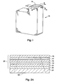
- Fig. 1 is a perspective view of an inkjet cartridge 10 with a printhead 14 of the present invention.
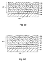
- FIGs. 2A and 2B illustrate side and front cross-sectional schematic partial views through A-A and B-B of Fig. 1 , respectively.
- a thin film stack 20 has been applied over a substrate 28.
- An area of a slot region 120 through the thin film stack 20 and the substrate 28 is shown in dashed lines.
- the slot region is extended through the thin film stack 20.
- the substrate is a monocrystalline silicon wafer as is known in the art. A wafer of approximately 525 microns for a four-inch diameter or approximately 625 microns for a six-inch diameter is appropriate.
- the silicon substrate is p-type, lightly doped to approximately 0.55 ohm/cm.
- the starting substrate may be glass, a semiconductive material, a Metal Matrix Composite (MMC), a Ceramic Matrix Composite (CMC), a Polymer Matrix Composite (PMC) or a sandwich Si/xMc, in which the x filler material is etched out of the composite matrix post vacuum processing.
- MMC Metal Matrix Composite
- CMC Ceramic Matrix Composite
- PMC Polymer Matrix Composite
- Si/xMc sandwich Si/xMc
- a capping layer 30 covers and seals the substrate 28, thereby providing a gas and liquid barrier layer. Because the capping layer 30 is a barrier layer, fluid is unable to flow into the substrate 28.
- Capping layer 30 may be formed of a variety of different materials such as silicon dioxide, aluminum oxide, silicon carbide, silicon nitride, and glass. The use of an electrically insulating dielectric material for capping layer 30 also serves to insulate substrate 28 from conductor traces -via interconnects (not shown).
- the capping layer may be formed using any of a variety of methods known to those of skill in the art such as sputtering, evaporation, and plasma enhanced chemical vapor deposition (PECVD).
- PECVD plasma enhanced chemical vapor deposition
- the thickness of capping layer 30 ay be any desired thickness sufficient to cover and seal the substrate. Generally, the capping layer has a thickness of up to about 1 to 2 microns.
- the capping layer is field oxide (FOX) 30 which is thermally grown 205 on the exposed substrate 28.
- the process grows the FOX into the silicon substrate as well as depositing it on top to form a total depth of approximately 1.3 microns. Because the FOX layer pulls the silicon from the substrate, a strong chemical bond is established between the FOX layer and the substrate. This layer will isolate the MOSFETs, to be formed, from each other and serves as part of the thermal inkjet heater resistor oxide underlayer.
- FOX field oxide
- a phosphorous-doped (n+) silicon dioxide interdielectric, insulating glass layer (PSG) 32 is deposited by PECVD techniques.
- the PSG layer has a thickness of up to about 1 to 2 microns. In one embodiment, this layer is approximately 0.5 micron thick and forms the remainder of the thermal inkjet heater resistor oxide underlayer. In another embodiment, the thickness range is about 0.7 to 0.9 microns.
- a mask is applied and the PSG layer etched to provide openings in the PSG for interconnect vias for the MOSFET.
- Another mask is applied and etched to allow for connection to the base silicon substrate 28.
- the formation and use of the vias is set forth in U.S. Pat. No. 4,862,197 to Stoffel (assigned to the common assignee herein) for a "Process for Manufacturing Thermal Ink Jet Printhead and Integrated Circuit (IC) Structures Produced Thereby,".
- Firing resistors are formed by depositing a layer of resistive materials 114 over the structure.
- sputter deposition techniques are used to deposit a layer of tantalum aluminum 114 composite across the structure.
- the composite has a resistivity of approximately 30 ohms/square.
- the resistor layer has a thickness of up to about 1 to 2 microns.
- resistive materials are known to those of skill in the art including tantalum aluminum, nickel chromium, and titanium nitride, which may optionally be doped with suitable impurities such as oxygen, nitrogen, and carbon, to adjust the resistivity of the material.
- the resistive material may be deposited by any suitable method such as sputtering, and evaporation.
- the resistor layer has a thickness in the range of about 100 angstroms to 300 angstroms. However, resistor layers with thicknesses outside this range are also within the scope of the invention.
- a conductive layer 115 is applied over the resistive material 114.
- the conductive layer may be formed of any of a variety of different materials including aluminum/copper (4%), copper, and gold, and may be deposited by any method, such as sputtering and evaporation. Generally, the conductive layer has a thickness of up to about 1 to 2 microns. In one embodiment, sputter deposition is used to deposit a layer of aluminum 115 to a thickness of approximately 0.5 micron.
- the resistive layer 114 and the conductive layer 115 are patterned, such as by photolithography, and etched. As shown in Fig. 3 and in Fig. 4 , an area of the conductor layer 115 has been etched out to form individual resistors 134 from the resistor layer 114 underneath the conductor traces 115. In one embodiment, a mask is applied and etched to define the resistor heater width and conductor traces. A subsequent mask is used similarly to define the heater resistor length and aluminum conductor 115 terminations.
- An insulating passivation layer 117 is formed over the resistors and conductor traces to prevent electrical charging of the fluid or corrosion of the device, in the event that an electrically conductive fluid is used.
- Passivation layer 117 may be formed of any suitable material such as silicon dioxide, aluminum oxide, silicon carbide, silicon nitride, and glass, and by any suitable method such as sputtering, evaporation, and PECVD. Generally, the passivation layer has a thickness of up to about 1 to 2 microns.
- a PECVD process is used to deposit a composite silicon nitride/silicon carbide layer 117 to serve as component passivation.
- This passivation layer 117 has a thickness of approximately 0.75 micron. In another embodiment, the thickness is about 0.4 microns.
- the surface of the structure is masked and etched to create vias for metal interconnects. In one embodiment, the passivation layer places the structure under compressive stress.
- a cavitation barrier layer 119 is added over the passivation layer 117.
- the cavitation barrier layer 119 helps dissipate the force of the collapsing drive bubble left in the wake of each ejected fluid drop.
- the cavitation barrier layer has a thickness of up to about 1 to 2 microns.
- the cavitation barrier layer is tantalum.
- the tantalum layer 119 is approximately 0.6 micron thick and serves as a passivation, anti-cavitation, and adhesion layer.
- the cavitation barrier layer absorbs energy away from the substrate during slot formation. Tantalum is a tough, ductile material that is deposited in the beta phase.
- the grain structure of the material is such that the layer also places the structure under compressive stress.
- the tantalum layer is sputter deposited quickly thereby holding the molecules in the layer in place. However, if the tantalum layer is annealed, the compressive stress is relieved.
- a drill slot 122 is formed in the substrate and thin film stack in the general area of the slot region 120.
- One method of forming the drill slot is abrasive sand blasting.
- a blasting apparatus uses a source of pressurized gas (e.g. compressed air) to eject abrasive particles toward the substrate coated with thin film layers to form the slot.
- the gas stream carries the particles from the apparatus at a high flow rate (e.g. a flow rate of about 2-20 grams/minute). The particles then contact the coated substrate, causing the formation of an opening therethrough.
- Abrasive particles range in size from about 10-200 microns in diameter.
- Abrasive particles include aluminum oxide, glass beads, silicon carbide, sodium bicarbonate, dolomite, and walnut shells.
- abrasive sand blasting uses aluminum oxide particles directed towards the slot region 120. Pressure of about 560 to 610 kPa is used in sand blasting. The type of sand that is used is 250 OPT.
- Substrates including metals, plastics, glass, and silicon, may have slots formed therethrough in the present invention.
- the invention shall not be limited to the cutting of any specific substrate material.
- the invention shall not be limited to the use of any particular abrasive powder. A wide variety of different systems and powders may be used.
- a polymer barrier layer 124 is deposited over the cavitation barrier layer 119.
- the barrier layer has a thickness of up to about 20 microns.
- the barrier layer 128 is comprised of a fast crosslinking polymer such as photoimagable epoxy (such as SU8 developed by IBM), photoimagable polymer or photosensitive silicone dielectrics, such as SINR-3010 manufactured by ShinEtsuTM.
- the barrier layer 124 is made of an organic polymer plastic which is substantially inert to the corrosive action of ink.
- Plastic polymers suitable for this purpose include products sold under the trademarks VACREL and RISTON by E. I. DuPont de Nemours and Co. of Wilmington, Del.
- the barrier layer 124 has a thickness of about 20 to 30 microns.
- the barrier layer 124 is applied and patterned before the slot is drilled.
- the drill slot region 120 ends in the cavitation barrier layer 119, as shown in Fig. 2B .
- the slot region 120 extends through the barrier layer 124, as shown in Fig. 2C .
- the abrasive sand blasting process is applied through the barrier layer 124.
- the properties in the material of the barrier aid in reducing the number of chips in the shelf in slot formation.
- the polymer barrier material absorbs energy away from the substrate during slot formation, thereby dampening the effect on the substrate structure. Crack propagation through the substrate, and chipping in the shelf tends to slow, and reduce, as a result.
- the barrier layer 124 includes orifices through which fluid is ejected, as discussed in this application.
- an orifice layer is applied over the barrier layer thereby forming orifices over firing chambers 132, as described in more detail below.
- Fig. 4 illustrates the structure of Fig. 3 through section C-C (the barrier layer), a plan view of the coated substrate.
- the substrate usually has a rectangular shape, with the slot 122 disposed longitudinally therein, as shown in Fig. 4 .
- the plastic barrier layer 124 is masked and etched 224 to define a shelf 128, fluid flow channels 130, and firing chambers 132.
- the shelf 128 surrounds the slot 122 and extends to the channels 130.
- Each firing chamber 132 has at least one fluid channel 130.
- the fluid channels 130 in the barrier layer have entrances for the fluid running along the shelf 128. As shown by directional arrows illustrated in Fig.
- a fluid supply (not shown) is below the substrate 28 and is pressurized to flow up through the drill slot 122 and into the firing chambers 132. As shown in the arrow of Fig. 4 , the fluid channels direct fluid from the slot to corresponding firing chambers 132.
- each firing chamber 132 is a heating element 134 that is formed of the resistive material layer 114 and coated with passivation and cavitation barrier layers (shown in Fig. 3 ). Propagation of a current or a "fire signal" through a heating element causes fluid in the corresponding firing chamber to be heated and expelled through a corresponding nozzle.
- the heating elements 134 and the corresponding firing chambers 132 are arranged in rows located on both sides of the slot 122 and are spaced approximately equal distances from the slot so that the ink channel length at each resistor is approximately equal.
- the width of the print swath achieved by one pass of a printhead is approximately equal to the length of the resistor rows, which in turn is approximately equal to the length of the slot.
- multi-slotted dies there are multi-slotted dies, and dies that are adjacent each other in the printhead 14.
- Slot to slot distance within a multi-slotted die, and from die to die, is decreased by up to approximately 20% due to the decrease in chip size and number in the shelf using the present invention of coating the substrate before forming the slot.
- Drill yield (the number of die that are within specification limits after drilling) increased by up to about 25-27% using the method of the present invention.
- the chip yield loss (the yield loss due to chipping) also decreased by up to about 30%.
- the high correlation between the drill yield and chip yield loss is due to the fact that chipping is the largest yield loss factor.
- the slot yield was approximately 83%.
- the slot yield was approximately 87%. The percentage difference between the first and second embodiments is statistically significant at the 95% confidence level.
- the slot yield was approximately 88%.
- the thin film layers applied over the substrate before drilling reduces the number of chips by up to about 90%.
- the number of chips greater in length than about 1 ⁇ 4 of a slot width is less than or equal to about 40.
- a slot width is typically about 150 to 200 microns.
- slot width is about 170 microns, and the length of the chips counted is about 40 microns.
- the number of chips is less than or equal to about 10.
- FOX, passivation, aluminum, tantalum aluminum and tantalum is deposited over the silicon substrate, a chip count is between about 10 chips and about 30 chips.
- GOX Gate Oxide
- Gold polymer layers used for barrier materials
- polysilicon may be deposited over the substrate.
- one layer is applied over the substrate.
- more than one layer is applied over the substrate.
- the present invention is not limited to the order of the layers illustrated.
- the present invention includes placing the above-mentioned layers in any order.
- one or more of the following layers may be applied over the substrate: a layer of ductile material, a metal, a material under compression, a resistive material (such as tantalum aluminum), a conductive material (such as aluminum), a cavitation barrier layer (such as tantalum), a passivation layer (such as silicon nitride and silicon carbide), an insulating layer grown from the substrate (such as FOX), PSG, a polymer layer, and a dielectric layer, in any combination.
- a layer of ductile material such as tantalum aluminum
- a conductive material such as aluminum
- a cavitation barrier layer such as tantalum
- a passivation layer such as silicon nitride and silicon carbide
- an insulating layer grown from the substrate such
- the thickness of the thin film stack over the slot region ranges from 0.25 micron up to about 50 microns. In another embodiment, the thickness of the film is at least about 2 1 ⁇ 2 microns. In another embodiment, the thickness of the film is at least about 3 microns.
- the slot in the substrate may be formed by another mechanical method, such as diamond saw cutting.
Landscapes
- Engineering & Computer Science (AREA)
- Manufacturing & Machinery (AREA)
- Particle Formation And Scattering Control In Inkjet Printers (AREA)
Claims (7)
- Ein Verfahren zum Bilden des geschlitzten Substrats (28) eines Mittelzuführungsdruckkopfs, wobei das Verfahren folgende Schritte aufweist:Aufbringen eines Dünnfilms (20, 30, 32, 114, 115, 117, 119 und/oder 124) über einem Substrat (28); undmechanisches Bilden eines Zuführungsschlitzes (122) in dem Substrat (28) und dem Dünnfilm (20, 30, 32, 114, 115, 117, 119 und/oder 124) durch eine Schlitzregion (120), die sich durch das Substrat (28) und den Dünnfilm (20, 30, 32, 114, 115, 117, 119 und/oder 124) erstreckt.
- Das Verfahren gemäß Anspruch 1, bei dem der Dünnfilm ein Metallfilm (114, 115 und/oder 119) ist.
- Das Verfahren gemäß Anspruch 1, bei dem der Dünnfilm ein Polymerfilm (124) ist.
- Das Verfahren gemäß Anspruch 1, bei dem der Dünnfilm ein dielektrischer Film (30, 32 und/oder 124) ist.
- Das Verfahren gemäß Anspruch 1, bei dem der Dünnfilm ein duktiles Material ist.
- Das Verfahren gemäß Anspruch 1, bei dem der aufgebrachte Dünnfilm unter Kompression steht.
- Das Verfahren gemäß Anspruch 1, bei dem der Zuführungsschlitz (122) durch abrasives Sandstrahlen gebildet ist.
Priority Applications (1)
| Application Number | Priority Date | Filing Date | Title |
|---|---|---|---|
| EP08075640A EP2000309A3 (de) | 2001-01-30 | 2002-01-21 | Dünnfilmbeschichtung eines geschlitzten Substrats und Techniken zum Bilden von geschlitzten Substraten |
Applications Claiming Priority (2)
| Application Number | Priority Date | Filing Date | Title |
|---|---|---|---|
| US09/772,752 US6648732B2 (en) | 2001-01-30 | 2001-01-30 | Thin film coating of a slotted substrate and techniques for forming slotted substrates |
| US772752 | 2004-02-05 |
Related Child Applications (1)
| Application Number | Title | Priority Date | Filing Date |
|---|---|---|---|
| EP08075640A Division EP2000309A3 (de) | 2001-01-30 | 2002-01-21 | Dünnfilmbeschichtung eines geschlitzten Substrats und Techniken zum Bilden von geschlitzten Substraten |
Publications (2)
| Publication Number | Publication Date |
|---|---|
| EP1226947A1 EP1226947A1 (de) | 2002-07-31 |
| EP1226947B1 true EP1226947B1 (de) | 2008-10-15 |
Family
ID=25096103
Family Applications (2)
| Application Number | Title | Priority Date | Filing Date |
|---|---|---|---|
| EP02250377A Expired - Lifetime EP1226947B1 (de) | 2001-01-30 | 2002-01-21 | Dünnfilmbeschichtung eines geschlitzen Substrates und Verfahren zur Herstellung von geschlitzten Substraten |
| EP08075640A Withdrawn EP2000309A3 (de) | 2001-01-30 | 2002-01-21 | Dünnfilmbeschichtung eines geschlitzten Substrats und Techniken zum Bilden von geschlitzten Substraten |
Family Applications After (1)
| Application Number | Title | Priority Date | Filing Date |
|---|---|---|---|
| EP08075640A Withdrawn EP2000309A3 (de) | 2001-01-30 | 2002-01-21 | Dünnfilmbeschichtung eines geschlitzten Substrats und Techniken zum Bilden von geschlitzten Substraten |
Country Status (4)
| Country | Link |
|---|---|
| US (2) | US6648732B2 (de) |
| EP (2) | EP1226947B1 (de) |
| JP (1) | JP4166476B2 (de) |
| DE (1) | DE60229316D1 (de) |
Families Citing this family (11)
| Publication number | Priority date | Publication date | Assignee | Title |
|---|---|---|---|---|
| KR100335311B1 (ko) * | 1994-09-13 | 2002-11-14 | 주식회사 디피아이 | 내가스체킹성아크릴수지조성물을포함하는도료조성물 |
| US6648732B2 (en) * | 2001-01-30 | 2003-11-18 | Hewlett-Packard Development Company, L.P. | Thin film coating of a slotted substrate and techniques for forming slotted substrates |
| JP2004130579A (ja) * | 2002-10-09 | 2004-04-30 | Sony Corp | 液体吐出ヘッド、液体吐出装置及び液体吐出ヘッドの製造方法 |
| JP2004230770A (ja) * | 2003-01-31 | 2004-08-19 | Fuji Photo Film Co Ltd | インクジェットヘッド |
| US7594328B2 (en) * | 2003-10-03 | 2009-09-29 | Hewlett-Packard Development Company, L.P. | Method of forming a slotted substrate with partially patterned layers |
| US7784916B2 (en) * | 2006-09-28 | 2010-08-31 | Lexmark International, Inc. | Micro-fluid ejection heads with multiple glass layers |
| US8454149B2 (en) * | 2009-06-29 | 2013-06-04 | Videojet Technologies Inc | Thermal inkjet print head with solvent resistance |
| US8382253B1 (en) | 2011-08-25 | 2013-02-26 | Hewlett-Packard Development Company, L.P. | Fluid ejection device and methods of fabrication |
| US8727499B2 (en) | 2011-12-21 | 2014-05-20 | Hewlett-Packard Development Company, L.P. | Protecting a fluid ejection device resistor |
| US9016836B2 (en) | 2013-05-14 | 2015-04-28 | Stmicroelectronics, Inc. | Ink jet printhead with polarity-changing driver for thermal resistors |
| US9016837B2 (en) | 2013-05-14 | 2015-04-28 | Stmicroelectronics, Inc. | Ink jet printhead device with compressive stressed dielectric layer |
Family Cites Families (18)
| Publication number | Priority date | Publication date | Assignee | Title |
|---|---|---|---|---|
| US2989046A (en) * | 1958-06-05 | 1961-06-20 | Paramount Pictures Corp | Method for drilling finished holes in glass |
| DE2604939C3 (de) | 1976-02-09 | 1978-07-27 | Ibm Deutschland Gmbh, 7000 Stuttgart | Verfahren zum Herstellen von wenigstens einem Durchgangsloch insbesondere einer Düse für Tintenstrahldrucker |
| US4239954A (en) * | 1978-12-11 | 1980-12-16 | United Technologies Corporation | Backer for electron beam hole drilling |
| US4894664A (en) | 1986-04-28 | 1990-01-16 | Hewlett-Packard Company | Monolithic thermal ink jet printhead with integral nozzle and ink feed |
| US4862197A (en) | 1986-08-28 | 1989-08-29 | Hewlett-Packard Co. | Process for manufacturing thermal ink jet printhead and integrated circuit (IC) structures produced thereby |
| IT1234800B (it) * | 1989-06-08 | 1992-05-27 | C Olivetti & C Spa Sede Via Je | Procedimento di fabbricazione di testine termiche di stampa a getto d'inchiostro e testine cosi' ottenute |
| GB2241186A (en) | 1990-02-24 | 1991-08-28 | Rolls Royce Plc | Anti-sputtercoating |
| US5105588A (en) * | 1990-09-10 | 1992-04-21 | Hewlett-Packard Company | Method and apparatus for simultaneously forming a plurality of openings through a substrate |
| US5703631A (en) | 1992-05-05 | 1997-12-30 | Compaq Computer Corporation | Method of forming an orifice array for a high density ink jet printhead |
| JP3196796B2 (ja) | 1992-06-24 | 2001-08-06 | セイコーエプソン株式会社 | インクジェット記録ヘッドのノズル形成方法 |
| US5308442A (en) | 1993-01-25 | 1994-05-03 | Hewlett-Packard Company | Anisotropically etched ink fill slots in silicon |
| BE1007894A3 (nl) * | 1993-12-20 | 1995-11-14 | Philips Electronics Nv | Werkwijze voor het vervaardigen van een plaat van niet-metallisch materiaal met een patroon van gaten en/of holten. |
| JPH08267753A (ja) * | 1995-03-29 | 1996-10-15 | Brother Ind Ltd | ノズルの製造方法 |
| US5658471A (en) | 1995-09-22 | 1997-08-19 | Lexmark International, Inc. | Fabrication of thermal ink-jet feed slots in a silicon substrate |
| KR100311880B1 (ko) | 1996-11-11 | 2001-12-20 | 미다라이 후지오 | 관통구멍의제작방법,관통구멍을갖는실리콘기판,이기판을이용한디바이스,잉크제트헤드의제조방법및잉크제트헤드 |
| US6238269B1 (en) * | 2000-01-26 | 2001-05-29 | Hewlett-Packard Company | Ink feed slot formation in ink-jet printheads |
| FR2811588B1 (fr) * | 2000-07-13 | 2002-10-11 | Centre Nat Rech Scient | Tete d'injection et de dosage thermique, son procede de fabrication et systeme de fonctionnalisation ou d'adressage la comprenant |
| US6648732B2 (en) * | 2001-01-30 | 2003-11-18 | Hewlett-Packard Development Company, L.P. | Thin film coating of a slotted substrate and techniques for forming slotted substrates |
-
2001
- 2001-01-30 US US09/772,752 patent/US6648732B2/en not_active Expired - Fee Related
-
2002
- 2002-01-21 EP EP02250377A patent/EP1226947B1/de not_active Expired - Lifetime
- 2002-01-21 DE DE60229316T patent/DE60229316D1/de not_active Expired - Lifetime
- 2002-01-21 JP JP2002011197A patent/JP4166476B2/ja not_active Expired - Fee Related
- 2002-01-21 EP EP08075640A patent/EP2000309A3/de not_active Withdrawn
-
2003
- 2003-10-03 US US10/679,097 patent/US6945634B2/en not_active Expired - Fee Related
Also Published As
| Publication number | Publication date |
|---|---|
| EP2000309A2 (de) | 2008-12-10 |
| US6945634B2 (en) | 2005-09-20 |
| EP2000309A3 (de) | 2009-12-16 |
| US6648732B2 (en) | 2003-11-18 |
| JP4166476B2 (ja) | 2008-10-15 |
| US20040067319A1 (en) | 2004-04-08 |
| JP2002248777A (ja) | 2002-09-03 |
| US20020102918A1 (en) | 2002-08-01 |
| EP1226947A1 (de) | 2002-07-31 |
| DE60229316D1 (de) | 2008-11-27 |
Similar Documents
| Publication | Publication Date | Title |
|---|---|---|
| US6890062B2 (en) | Heater chip configuration for an inkjet printhead and printer | |
| KR20060115386A (ko) | 박막을 구비한 프린트 헤드 | |
| EP1226947B1 (de) | Dünnfilmbeschichtung eines geschlitzen Substrates und Verfahren zur Herstellung von geschlitzten Substraten | |
| EP1125746B1 (de) | Struktur zum Bewirken einer Haftung zwischen dem Substrat und der Tintensperre in einem Tintenstrahldruckkopf | |
| US6513913B2 (en) | Heating element of a printhead having conductive layer between resistive layers | |
| US7914123B2 (en) | Inkjet printhead and manufacturing method thereof | |
| US20100321447A1 (en) | Protective layers for micro-fluid ejection devices and methods for depositing same | |
| KR20040034250A (ko) | 테이퍼 형상의 노즐을 가진 일체형 잉크젯 프린트헤드 및그 제조방법 | |
| US7198358B2 (en) | Heating element, fluid heating device, inkjet printhead, and print cartridge having the same and method of making the same | |
| KR100501859B1 (ko) | 잉크젯 헤드 및 이의 제조 방법 | |
| EP3634763B1 (de) | Flüssigkeitsausstossvorrichtung mit verringertem überlagerung, entsprechendes betriebsverfahren und herstellungsverfahren | |
| US7594328B2 (en) | Method of forming a slotted substrate with partially patterned layers | |
| JP2004237732A (ja) | インクジェットプリントヘッド及びその製造方法 | |
| KR100553912B1 (ko) | 잉크젯 프린트헤드 및 그 제조방법 | |
| KR20040101862A (ko) | 잉크젯 프린트헤드 및 그 제조방법 | |
| JP2004130809A (ja) | 金属ノズルプレートを有した一体型インクジェットプリントヘッド及びその製造方法 | |
| KR100499150B1 (ko) | 잉크젯 프린트헤드 및 그 제조방법 | |
| US6834941B1 (en) | Heater chip configuration for an inkjet printhead and printer | |
| JPH07125210A (ja) | サーマルインクジェットヘッド | |
| JP2008149666A (ja) | インクジェット記録ヘッド | |
| JP2008120003A (ja) | インクジェット記録ヘッドおよび該へッド用基板の製造方法 | |
| JP2007283669A (ja) | インクジェット記録ヘッド、インクジェット記録ヘッドの製造方法 | |
| JP2007276150A (ja) | インクジェット記録ヘッドおよびインクジェット記録ヘッドの製造方法 | |
| JPH06320730A (ja) | サーマルインクジェットヘッド | |
| JP2003226021A (ja) | インクジェットヘッドおよびインクジェットヘッドの製造方法 |
Legal Events
| Date | Code | Title | Description |
|---|---|---|---|
| PUAI | Public reference made under article 153(3) epc to a published international application that has entered the european phase |
Free format text: ORIGINAL CODE: 0009012 |
|
| AK | Designated contracting states |
Kind code of ref document: A1 Designated state(s): AT BE CH CY DE DK ES FI FR GB GR IE IT LI LU MC NL PT SE TR |
|
| AX | Request for extension of the european patent |
Free format text: AL;LT;LV;MK;RO;SI |
|
| 17P | Request for examination filed |
Effective date: 20030107 |
|
| AKX | Designation fees paid |
Designated state(s): DE FR GB NL |
|
| 17Q | First examination report despatched |
Effective date: 20050427 |
|
| 17Q | First examination report despatched |
Effective date: 20050427 |
|
| GRAP | Despatch of communication of intention to grant a patent |
Free format text: ORIGINAL CODE: EPIDOSNIGR1 |
|
| GRAS | Grant fee paid |
Free format text: ORIGINAL CODE: EPIDOSNIGR3 |
|
| GRAA | (expected) grant |
Free format text: ORIGINAL CODE: 0009210 |
|
| AK | Designated contracting states |
Kind code of ref document: B1 Designated state(s): DE FR GB NL |
|
| REG | Reference to a national code |
Ref country code: GB Ref legal event code: FG4D |
|
| REF | Corresponds to: |
Ref document number: 60229316 Country of ref document: DE Date of ref document: 20081127 Kind code of ref document: P |
|
| PLBE | No opposition filed within time limit |
Free format text: ORIGINAL CODE: 0009261 |
|
| STAA | Information on the status of an ep patent application or granted ep patent |
Free format text: STATUS: NO OPPOSITION FILED WITHIN TIME LIMIT |
|
| 26N | No opposition filed |
Effective date: 20090716 |
|
| PGFP | Annual fee paid to national office [announced via postgrant information from national office to epo] |
Ref country code: FR Payment date: 20100205 Year of fee payment: 9 |
|
| PGFP | Annual fee paid to national office [announced via postgrant information from national office to epo] |
Ref country code: DE Payment date: 20100127 Year of fee payment: 9 Ref country code: GB Payment date: 20100125 Year of fee payment: 9 |
|
| PGFP | Annual fee paid to national office [announced via postgrant information from national office to epo] |
Ref country code: NL Payment date: 20100124 Year of fee payment: 9 |
|
| REG | Reference to a national code |
Ref country code: NL Ref legal event code: V1 Effective date: 20110801 |
|
| GBPC | Gb: european patent ceased through non-payment of renewal fee |
Effective date: 20110121 |
|
| REG | Reference to a national code |
Ref country code: FR Ref legal event code: ST Effective date: 20110930 |
|
| PG25 | Lapsed in a contracting state [announced via postgrant information from national office to epo] |
Ref country code: FR Free format text: LAPSE BECAUSE OF NON-PAYMENT OF DUE FEES Effective date: 20110131 |
|
| PG25 | Lapsed in a contracting state [announced via postgrant information from national office to epo] |
Ref country code: GB Free format text: LAPSE BECAUSE OF NON-PAYMENT OF DUE FEES Effective date: 20110121 |
|
| REG | Reference to a national code |
Ref country code: DE Ref legal event code: R119 Ref document number: 60229316 Country of ref document: DE Effective date: 20110802 |
|
| PG25 | Lapsed in a contracting state [announced via postgrant information from national office to epo] |
Ref country code: NL Free format text: LAPSE BECAUSE OF NON-PAYMENT OF DUE FEES Effective date: 20110801 |
|
| PG25 | Lapsed in a contracting state [announced via postgrant information from national office to epo] |
Ref country code: DE Free format text: LAPSE BECAUSE OF NON-PAYMENT OF DUE FEES Effective date: 20110802 |