EP1226348B1 - Ansteuereinheit für ein kapazitives stellglied - Google Patents
Ansteuereinheit für ein kapazitives stellglied Download PDFInfo
- Publication number
- EP1226348B1 EP1226348B1 EP00987071A EP00987071A EP1226348B1 EP 1226348 B1 EP1226348 B1 EP 1226348B1 EP 00987071 A EP00987071 A EP 00987071A EP 00987071 A EP00987071 A EP 00987071A EP 1226348 B1 EP1226348 B1 EP 1226348B1
- Authority
- EP
- European Patent Office
- Prior art keywords
- charging
- reference signal
- switch
- transformer
- voltage
- Prior art date
- Legal status (The legal status is an assumption and is not a legal conclusion. Google has not performed a legal analysis and makes no representation as to the accuracy of the status listed.)
- Expired - Lifetime
Links
Images



Classifications
-
- F—MECHANICAL ENGINEERING; LIGHTING; HEATING; WEAPONS; BLASTING
- F02—COMBUSTION ENGINES; HOT-GAS OR COMBUSTION-PRODUCT ENGINE PLANTS
- F02D—CONTROLLING COMBUSTION ENGINES
- F02D41/00—Electrical control of supply of combustible mixture or its constituents
- F02D41/20—Output circuits, e.g. for controlling currents in command coils
- F02D41/2096—Output circuits, e.g. for controlling currents in command coils for controlling piezoelectric injectors
-
- H—ELECTRICITY
- H02—GENERATION; CONVERSION OR DISTRIBUTION OF ELECTRIC POWER
- H02N—ELECTRIC MACHINES NOT OTHERWISE PROVIDED FOR
- H02N2/00—Electric machines in general using piezoelectric effect, electrostriction or magnetostriction
- H02N2/02—Electric machines in general using piezoelectric effect, electrostriction or magnetostriction producing linear motion, e.g. actuators; Linear positioners ; Linear motors
- H02N2/06—Drive circuits; Control arrangements or methods
- H02N2/065—Large signal circuits, e.g. final stages
-
- H—ELECTRICITY
- H10—SEMICONDUCTOR DEVICES; ELECTRIC SOLID-STATE DEVICES NOT OTHERWISE PROVIDED FOR
- H10N—ELECTRIC SOLID-STATE DEVICES NOT OTHERWISE PROVIDED FOR
- H10N30/00—Piezoelectric or electrostrictive devices
- H10N30/80—Constructional details
- H10N30/802—Circuitry or processes for operating piezoelectric or electrostrictive devices not otherwise provided for, e.g. drive circuits
-
- F—MECHANICAL ENGINEERING; LIGHTING; HEATING; WEAPONS; BLASTING
- F02—COMBUSTION ENGINES; HOT-GAS OR COMBUSTION-PRODUCT ENGINE PLANTS
- F02D—CONTROLLING COMBUSTION ENGINES
- F02D41/00—Electrical control of supply of combustible mixture or its constituents
- F02D41/20—Output circuits, e.g. for controlling currents in command coils
- F02D2041/2003—Output circuits, e.g. for controlling currents in command coils using means for creating a boost voltage, i.e. generation or use of a voltage higher than the battery voltage, e.g. to speed up injector opening
- F02D2041/2006—Output circuits, e.g. for controlling currents in command coils using means for creating a boost voltage, i.e. generation or use of a voltage higher than the battery voltage, e.g. to speed up injector opening by using a boost capacitor
-
- F—MECHANICAL ENGINEERING; LIGHTING; HEATING; WEAPONS; BLASTING
- F02—COMBUSTION ENGINES; HOT-GAS OR COMBUSTION-PRODUCT ENGINE PLANTS
- F02D—CONTROLLING COMBUSTION ENGINES
- F02D41/00—Electrical control of supply of combustible mixture or its constituents
- F02D41/20—Output circuits, e.g. for controlling currents in command coils
- F02D2041/2003—Output circuits, e.g. for controlling currents in command coils using means for creating a boost voltage, i.e. generation or use of a voltage higher than the battery voltage, e.g. to speed up injector opening
- F02D2041/2013—Output circuits, e.g. for controlling currents in command coils using means for creating a boost voltage, i.e. generation or use of a voltage higher than the battery voltage, e.g. to speed up injector opening by using a boost voltage source
-
- F—MECHANICAL ENGINEERING; LIGHTING; HEATING; WEAPONS; BLASTING
- F02—COMBUSTION ENGINES; HOT-GAS OR COMBUSTION-PRODUCT ENGINE PLANTS
- F02D—CONTROLLING COMBUSTION ENGINES
- F02D41/00—Electrical control of supply of combustible mixture or its constituents
- F02D41/20—Output circuits, e.g. for controlling currents in command coils
- F02D2041/202—Output circuits, e.g. for controlling currents in command coils characterised by the control of the circuit
- F02D2041/2024—Output circuits, e.g. for controlling currents in command coils characterised by the control of the circuit the control switching a load after time-on and time-off pulses
- F02D2041/2027—Control of the current by pulse width modulation or duty cycle control
-
- F—MECHANICAL ENGINEERING; LIGHTING; HEATING; WEAPONS; BLASTING
- F02—COMBUSTION ENGINES; HOT-GAS OR COMBUSTION-PRODUCT ENGINE PLANTS
- F02D—CONTROLLING COMBUSTION ENGINES
- F02D41/00—Electrical control of supply of combustible mixture or its constituents
- F02D41/20—Output circuits, e.g. for controlling currents in command coils
- F02D2041/202—Output circuits, e.g. for controlling currents in command coils characterised by the control of the circuit
- F02D2041/2034—Control of the current gradient
-
- F—MECHANICAL ENGINEERING; LIGHTING; HEATING; WEAPONS; BLASTING
- F02—COMBUSTION ENGINES; HOT-GAS OR COMBUSTION-PRODUCT ENGINE PLANTS
- F02D—CONTROLLING COMBUSTION ENGINES
- F02D41/00—Electrical control of supply of combustible mixture or its constituents
- F02D41/20—Output circuits, e.g. for controlling currents in command coils
- F02D2041/202—Output circuits, e.g. for controlling currents in command coils characterised by the control of the circuit
- F02D2041/2041—Output circuits, e.g. for controlling currents in command coils characterised by the control of the circuit for controlling the current in the free-wheeling phase
-
- F—MECHANICAL ENGINEERING; LIGHTING; HEATING; WEAPONS; BLASTING
- F02—COMBUSTION ENGINES; HOT-GAS OR COMBUSTION-PRODUCT ENGINE PLANTS
- F02D—CONTROLLING COMBUSTION ENGINES
- F02D41/00—Electrical control of supply of combustible mixture or its constituents
- F02D41/20—Output circuits, e.g. for controlling currents in command coils
- F02D2041/202—Output circuits, e.g. for controlling currents in command coils characterised by the control of the circuit
- F02D2041/2058—Output circuits, e.g. for controlling currents in command coils characterised by the control of the circuit using information of the actual current value
-
- F—MECHANICAL ENGINEERING; LIGHTING; HEATING; WEAPONS; BLASTING
- F02—COMBUSTION ENGINES; HOT-GAS OR COMBUSTION-PRODUCT ENGINE PLANTS
- F02D—CONTROLLING COMBUSTION ENGINES
- F02D41/00—Electrical control of supply of combustible mixture or its constituents
- F02D41/20—Output circuits, e.g. for controlling currents in command coils
- F02D2041/2068—Output circuits, e.g. for controlling currents in command coils characterised by the circuit design or special circuit elements
- F02D2041/2075—Type of transistors or particular use thereof
Definitions
- the invention relates to a device for variable control at least one capacitive actuator, in particular of a piezo actuator for a fuel injector in one Internal combustion engine, according to the preamble of the claim 1.
- Piezo drives in particular have proven to be advantageous here proved.
- Piezo drives In order to achieve the required stroke for piezo drives That is to be able to reach the nozzle needle in the fuel injector Piezo element generally from a stack of piezo ceramic disks composed over an electrical Parallel connection can be operated in order to ensure sufficient Needle stroke necessary to achieve high field strengths can.
- Such a multilayer piezo actuator provides for the electronic power amplifier used for control strong capacitive load that is in a very short span of time charged to a target voltage and then again must be unloaded.
- the power amplifier must guarantee that the piezo actuator is controlled so that the injected Fuel quantity from injection process to injection process remains exactly reproducible.
- the final stage should can control the piezo actuator so that in addition to the Main injection of smallest amounts of fuel before or after this main injection from the fuel injector into the combustion chamber be delivered.
- US 4,749,897 discloses a control circuit for a piezo actuator, in which a predetermined one during a charging process Energy amount by means of a transformer in one Swinging process is transmitted to the actuator and this unloaded again unregulated.
- piezoelectric fuel injectors are used for control preferably electronic power amplifiers used work on the principle of an LC resonant circuit in which the piezo actuator represents the capacitor.
- the loading process of the piezo actuator takes place as a reversing process the charge from a charge source via a charge transfer coil to the piezo actuator, the inductance of the recharge coil together with the capacities of the charge source and the Piezo actuator, the time constant for the charging or discharging process, d. H. determined for the loading or unloading time.
- a such final stage is u. a. in US 5,130,598.
- the charge source for LC elements is at least one half of the maximum actuator voltage supply the corresponding voltage can, which makes them very expensive. Will continue the piezo actuator is always charged to a nominal voltage, see above that fast loading and unloading are necessary to the desired small amounts of fuel via the fuel injector to be able to inject.
- Such quick loading and Discharging processes with high charging currents lead to a large stress on the piezo ceramic and moreover to a strong excitation of the resonance frequencies of the fuel injector, which can lead to high noise levels.
- the object of the present invention is a device for the variable control of a capacitive actuator, in particular to create a piezo actuator in which by means of a simple and inexpensive switching any gradients the charge or discharge voltage of the capacitive actuator possible are.
- the device according to the invention is characterized by a Fly-back converter with a transformer that allows those when a capacitive actuator is being charged, in particular a piezo actuator fed electrical Energy when discharging depends on the efficiency of the piezo actuator mostly recover it, store it in the converter and in the subsequent loading process z. B. the next capacitive actuator to reuse.
- the invention Device also has the advantage that a Energy source only a much lower voltage than that must generate the required voltage on the actuator, whereby the charging and discharging time and the voltage at the actuator generate a specific stroke, have it set as you like.
- the switch is the Loading and unloading devices each with a pulse width modulated Signal switched to a conductive state, wherein the pulse duty factor of the pulse-width modulated signal it is determined that the switch remains conductive until a comparison device determines that the switch measured current value corresponds to a reference current value.
- the charging transistor of the charging device being preferred is a normally-off field-effect transistor characterized by a low power loss, and wherein the switch of the discharge device is preferably a bipolar transistor with an insulated gate that has a high breakdown voltage has.
- the reference signal generated by a high pass filter that one of allows a constant value deviating reference signal curve.
- the high-pass filter can be used as an RC element for generation a logarithmic curve of the voltage at the capacitive Actuator or as an LC element to generate a sinusoidal Developed the course of the voltage on the capacitive actuator his.
- the reference signal generator can also have a digital / analog converter by a processor is driven to any reference signal waveform to create.
- the device shown in Figure 1 as a basic circuit for variable control of a capacitive actuator in the presented embodiment as an output stage for activation of a piezo element 1 is used.
- the final stage is from powered by a power source in the embodiment shown from an on-board electrical system voltage of 50 V to 80 V powered DC / DC converter 2 with adjustable output voltage consists of a charging capacitor 3 on each desired output voltage.
- first snubber circuit 61 is arranged, which consists of a Series connection of a resistor 611 and a capacitor 612 exists. This first snubber circuit 61 serves the by leakage inductances of the transformer 4 in the primary coil 41 to eliminate induced voltage peaks.
- a charging device is parallel to the first free-wheeling diode 51 7 switched.
- the charging device 7 has a series connection from a serving as a switch transistor 71 and a downstream one, designed as a current measuring resistor 72 Measuring device 71.
- the charging transistor 71 is in the Embodiment shown a self-locking MOSFET, the Source is connected in series with the primary coil 41.
- the The drain of the MOSFET is connected to the via the current measuring resistor 72 Reference potential GND connected.
- the gate of the charging transistor 71 is driven by a charging flip-flop 73.
- the voltage drop across the current measuring resistor 72 is about a low-pass filter 74 is tapped and into a comparison device the comparator 75 used, the current falling therefrom via the charging transistor 71 certainly.
- the low-pass filter 74 is used for current peaks that result from the switching processes of the charging transistor 71, filter out.
- the comparator 75 is still a reference signal generator 76 supplied with a reference signal that compared by the comparator 75 with the measured current value becomes.
- the reference signal generator 76 is activated via a charge control signal hard.
- the charging flip-flop 73 for driving the gate of the charging transistor 71 is always of a pulse width modulated Control signal triggered and by comparator 75 reset.
- the secondary coil 42 of the transformer 4 is opposite to Primary coil 41 wound and on one side to the as capacitive actuator acting piezo element 1 connected.
- a second freewheeling diode 52 is connected, which is of reference potential GND is conductive towards the secondary coil 42.
- Parallel to the secondary coil 42 of the transformer 4 is one arranged second snubber circuit 62, which consists of a Resistor 621 and a capacitor 622 is composed.
- the second snubber circuit 62 is used in the secondary coil 42 of the transformer 4 due to leakage inductances suppress induced voltage peaks.
- Parallel to A second discharge diode 52 is connected to a discharge device 8.
- the structure (not shown) of the unloading device 8 is preferably symmetrical to the charging device 7, however, a bipolar transistor is preferably used as the discharge transistor 81 with an insulated gate is used characterized by a high breakdown voltage.
- the control signals of the charging device 7 and the unloading device 8 are from a control circuit, not shown issued, which can be part of an engine control unit.
- the output stage shown in FIG. 1 for the piezo element 1 represents a fly-back converter, in which the at a Charging process fed into the piezo element 1 electrical Energy essentially recovered during discharge Switching power supply cached and for the following Switching process can be used.
- the charging flip-flop 73 When charging, the charging flip-flop 73 with a control signal in the form of a pulse width modulated signal with a predetermined frequency, typically in the range of 100 kHz, and a predetermined duty cycle, preferably 50%.
- the pulse width modulated signal sets the charging flip-flop 73 conductive with each pulse, causing the charging flip-flop 73 on the gate of the charging transistor 71, a pulsed charging signal is issued.
- the charging transistor 71 is turned on, so that a Charging current Id from the charging capacitor 3 via the primary coil 41 and the charging transistor 71 flows.
- the charging current Id increases because of the inductive load of the primary coil 41 of the transformer 4 linear.
- This charging current Id is on the Current measuring resistor 72 falling voltage from comparator 75 tapped, the low-pass filter 74 current peaks that are generated by the switching process of the charging transistor 71, suppressed.
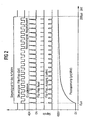
- the comparator 75 compares the measured current value with one Reference current value from the reference signal generator 76 during of the charging process is applied to the comparator 75. In In the embodiment shown in FIG. 2, this is the reference signal set to a constant value.
- the comparator provides 75 states that the measured charging current Id the predetermined Corresponds to the reference value is from the comparator 75 to the Load flip-flop 73 outputs a signal representing the load flip-flop 73 resets. Resetting the load flip-flop 73 causes the charge flip-flop 73 to the gate of the charge transistor 71 output charging signal is interrupted. The charging transistor 71 then blocks again and thus interrupts the charging current Id until the charging flip-flop 73 through the next control signal is retriggered.
- the transformer 4 By changing the charging current Id in the primary coil 41 the transformer 4, especially when the charging current is interrupted, is in the secondary coil 42 of the transformer 4th a the turns ratio of the primary coil 41 to the secondary coil 42 generates corresponding pulse-shaped voltage that is smoothed by a filter (not shown).
- a filter (not shown).
- the constant reference signal one constant per charging current pulse Energy pulse generated in the secondary coil 42 of the transformer 4. These constant energy pulses charge the piezo element 1 until the desired piezo voltage is reached at the end of the charging time is reached.
- the secondary circuit with the secondary coil 42 is about when loading the piezo element 1 the freewheeling diode 52 closed.
- the piezo element 1 is then also discharged with pulse width modulated signals of the discharge device 8, wherein which is designed as an insulated gate bipolar transistor Discharge transistor 81 conductive and non-conductive is controlled, whereby the voltage of the piezo element 1 to drops to zero.
- the discharge device 8 can be analog to the charging device 7 with a current measuring resistor, a low pass filter, a comparator, a reference signal generator and a flip-flop to the duty cycle the activation of the discharge transistor 81 via a measurement of the discharge current in the secondary circuit of the transformer 4 determine.
- By changing the discharge current via the control of the discharge transistor 81 becomes part of the discharge energy back to the primary side of the transformer 4 transferred and stored back in the charging capacitor 3.
- the Primary circuit with the charging capacitor 3 and the primary coil 41 of the transformer 4 closes via the freewheeling diode 51st
- the root-shaped course of the charging voltage shown in FIG. 2 allows the piezo element 1 with charging pulses more constant Charge energy so that peak currents in the piezo drive be avoided.
- the time course of the charging voltage can be optimized so that a sound development is suppressed on the piezo drive.
- the snubber circuits 61, 62 ensure that Voltage peaks due to leakage inductances in the primary coil 41 or the secondary coil 42, which leads to overvoltages could lead to be prevented.
- the snubber circuits 61, 62 could also, instead of parallel to the coils 41, 42 of the transformer 4, parallel to the charging device 7 or Unloading device 8 may be arranged.
- the Possibility instead of the freewheeling diodes 51, 52, the primary or Secondary circuit for voltage induction via transistors close synchronously.
- the as a charging transistor 71 in the charging device 7 used self-locking MOSFET is characterized by a low resistance to current flow between drain and source.
- MOSFETs also have the option of other transistor components or basically other switch types use. This also applies to the discharge switch 81 in the discharge circuit 8 used bipolar transistor with isolated Gate. This is preferred because it is characterized by a high breakdown voltage. A such high breakdown voltage is particularly due to the high voltages occurring on the secondary side are desirable.
- the constant reference signal of the reference signal generator 76 charging the piezo element 1 with constant Charge pulses reached, resulting in a root-shaped course of the charging voltage on the piezo element 1.
- the output stage shown in FIG. 1 also has the possibility of other time profiles of the voltage on the piezo element 1 to generate.
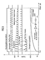
- FIG 3 are the signal curves corresponding to Figure 2 shown for a reference signal generator 76, which as an RC element is trained.
- This RC element consists of an inverter 761, a capacitor 762 and a resistor 763 together, which are connected in series, the reference signal tapped between capacitor 762 and resistor 763 becomes.
- This circuit leads to an exponential decreasing course of the reference signal and thus to a logarithmic rising curve of the charging voltage at the piezo element 1, as Figure 3 shows.
- This configuration will achieved that with the fly-back converter with pulse-width modulated Signal simulated the behavior of an RC power amplifier becomes.
- Figure 4 shows a further possible embodiment in which the reference signal generator 76 is designed as an RC element.
- the reference signal generator 76 is designed as an RC element.
- a coil 764 and a capacitor 765 are in series switched, the reference signal between coil 764 and the capacitor 765 is tapped.
- the fly-back converter thus simulates an LC power amplifier.
- reference signal generators 76 only allows a limited number of waveforms of the charging voltage or To generate discharge voltage at the piezo element 1.
- reference signal generator as a digital / analog converter 92 be designed, which is controlled by a microprocessor 91 is used to generate reference signals with any waveform produce.
- the coupling of the microprocessor 91 to the digital / analog converter 92 can, as shown in Figure 5B is done with a single 8-bit port.
- the essential The advantage of this arrangement is that the microprocessor 91 does not even include the pulse-width modulated signals each pulse newly calculated duty cycle, but a digital value to the digital / analog converter for each pulse 92 which then corresponds to the digital value Generated reference signal.
- the microprocessor 91 can also additionally the control signals for the charging flip-flop 73 or generate the discharge flip-flop 83 because these signals as simple pulse width modulated signals such. B. with a 50% duty cycle are designed.
- the one controlled by the microprocessor 91 can Digital / analog converter 92 as a common reference signal generator both for the charging device 7 and for the unloading device 8 are used, since these two signals only are needed at different times.
- Digital / analog converter 92 is one of the charger 7 corresponding discharge device 8 with the discharge flip-flop 83, a current measuring resistor 82, a low-pass filter 84 and a comparator 85.
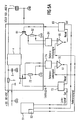
- the one in Figure 5A shown device works in principle similar to the output stage shown in Figure 1.
- the inventive design of a device for variable control of a capacitive actuator as Fly-back converter with a transformer in which the Duty cycle of the pulse width modulated signals for control of the charging or discharging transistor by measuring the respective currents takes place it is possible to use any shapes the charge or discharge voltage on the capacitive actuator to reach.
- Such a device is particularly suitable as a power amplifier for a piezo actuator.
Landscapes
- Engineering & Computer Science (AREA)
- Chemical & Material Sciences (AREA)
- Combustion & Propulsion (AREA)
- Mechanical Engineering (AREA)
- General Engineering & Computer Science (AREA)
- Electrical Control Of Air Or Fuel Supplied To Internal-Combustion Engine (AREA)
- General Electrical Machinery Utilizing Piezoelectricity, Electrostriction Or Magnetostriction (AREA)
Abstract
Description
- Figur 1
- ein Prinzipschaltbild einer ersten Ausführungsform der erfindungsgemäßen Vorrichtung mit einer Ladeeinrichtung;
- Figur 2
- ein Diagramm der Signalverläufe in der Vorrichtung nach Figur 1 für ein konstantes Referenzsignal;
- Figur 3
- ein Diagramm der Signalverläufe bei einem mit einem RC-Glied erzeugten Referenzsignal;
- Figur 4
- ein Diagramm der Signalverläufe bei einem mit einem LC-Glied erzeugten Referenzsignal;
- Figur 5A
- ein Prinzipschaltbild einer zweiten Ausführungsform der erfindungsgemäßen Vorrichtung mit einer Ladeund einer Entladeeinrichtung; und
- Figur 5B
- einen digitalen Referenzsignalgeber, wie er bei der in Figur 5A gezeigten Ausführungsform eingesetzt wird.
Claims (7)
- Vorrichtung zum variablen Ansteuern wenigstens eines kapazitiven Stellgliedes, insbesondere eines Piezoelements (1) in einem Kraftstoffinjektor, mit einem von einer Energiequelle (2) auf ein bezüglich eines Bezugspotentials vorgegebene Spannung aufladbaren Ladenkondensator (3),wobeiparallel zum Ladekondensator (3) eine Reihenschaltung der Primärspule (41) eines Transformators (4) und einer Ladeeinrichtung (7) angeordnet ist,die Sekundärspule (42) des Transformators (4) mit einer Entladeinrichtung (8) und dem kapazitiven Stellglied (1) in Reihe geschaltet ist.parallel zur Ladeeinrichtung (7) ein vom Bezugpotential (GND) weg stromleitendes Element (51) und parallel zur Entladeeinrichtung (8) ein vom Bezugspotential (GND) weg stromleitendes Element (8) geschaltet ist,die Ladeeinrichtung (7) und/oder Entladeeinrichtung 88) einen Schalter 871, 81), eine zwischen dem Schalter und dem Bezugspotential angeordnete Messeinrichtung (72, 82) zum Bestimmen des über den Schalter fließenden Stroms, einen Referenzsignalgeber (76, 92) zum Erzeugen eines Referenzstromwerte darstellenden Signalverlaufs, eine Vergleichseinrichtung (75, 85) zum Vergleichen des gemessenen Stromwertes mit dem Referenzsignal und eine Steuereinrichtung (73, 81) mit einem pulsweiten-modelierten Signal, um den Schalter in einen leitenden Zustand zu schalten, aufweist, wobei das Tastverhältnis des einem pulsweiten-modelierten Signals so bestimmt wird, dass der Schalter (71, 81) so lange leitend bleibt, bis die Vergleichseinrichtung (75, 85) feststellt, dass der gemessene Stromwert dem Referenzsignal entspricht, und wobei der Referenzsignalgeber (76) ein Hochpassfilter zum Erzeugen eines von einem konstanten Wert abweichenden Referenzsignalverlaufs aufweist.
- Vorrichtung nach Anspruch 1, dadurch gekennzeichnet, dass die Steuereinrichtung (73, 83) ein Flip-Flop zum Ansteuern des Schalters (71, 81) aufweist, wobei das Flip-Flop von einem konstanten Steuersignal getriggert wird und von der Vergleichseinrichtung (75, 85) zurückgesetzt wird, wenn der gemessene Stromwert dem Referenzsignal entspricht.
- Vorrichtung nach Anspruch 1, dadurch gekennzeichnet, dass der Referenzsignalgeber (76) ein RC-Glied zum Erzeugen eines logarithmischen Verlaufes der Lade- bzw. Entladespannung am kapazitiven Stellglied (1) aufweist.
- Vorrichtung nach Anspruch 1, dadurch gekennzeichnet, dass der Referenzsignalgeber 876) ein RC-Glied zum Erzeugen eines sinusförmigen Verlaufes der Lade- bzw. Entladespannung am kapazitiven Stellglied (1) aufweist.
- Vorrichtung nach Anspruch 1, dadurch gekennzeichnet, dass der Referenzsignalgeber (76) einen Digital/Analog-Wandler (2) aufweist, der von einem Mikroprozessor (91) angesteuert wird, um den Referenzsignalverlauf zu erzeugen.
- Vorrichtung nach Anspruch 1, dadurch gekennzeichnet, dass die Ladeeinrichtung (7) und die Entladeeinrichtung (8) einen gemeinsamen Referenzsignalgeber aufweisen.
- Vorrichtung nach Anspruch 1, dadurch gekennzeichnet, dass parallel zum Transformator 84) ein Snubber-Netzwerk geschaltet ist, um die durch Streuinduktivität im Transformator (4) erzeugten Spannungsspitzen zu dämpfen.
Applications Claiming Priority (3)
| Application Number | Priority Date | Filing Date | Title |
|---|---|---|---|
| DE19952950A DE19952950A1 (de) | 1999-11-03 | 1999-11-03 | Ansteuereinheit für ein kapazitives Stellglied |
| DE19952950 | 1999-11-03 | ||
| PCT/DE2000/003863 WO2001033061A1 (de) | 1999-11-03 | 2000-11-03 | Ansteuereinheit für ein kapazitives stellglied |
Publications (2)
| Publication Number | Publication Date |
|---|---|
| EP1226348A1 EP1226348A1 (de) | 2002-07-31 |
| EP1226348B1 true EP1226348B1 (de) | 2004-08-18 |
Family
ID=7927810
Family Applications (1)
| Application Number | Title | Priority Date | Filing Date |
|---|---|---|---|
| EP00987071A Expired - Lifetime EP1226348B1 (de) | 1999-11-03 | 2000-11-03 | Ansteuereinheit für ein kapazitives stellglied |
Country Status (3)
| Country | Link |
|---|---|
| EP (1) | EP1226348B1 (de) |
| DE (2) | DE19952950A1 (de) |
| WO (1) | WO2001033061A1 (de) |
Families Citing this family (26)
| Publication number | Priority date | Publication date | Assignee | Title |
|---|---|---|---|---|
| EP1563597A1 (de) * | 2002-09-05 | 2005-08-17 | Viking Technologies L.C. | Vorrichtung und verfahren zum laden und entladen eines kondensators |
| US6979933B2 (en) | 2002-09-05 | 2005-12-27 | Viking Technologies, L.C. | Apparatus and method for charging and discharging a capacitor |
| US7190102B2 (en) | 2002-09-05 | 2007-03-13 | Viking Technologies, L.C. | Apparatus and method for charging and discharging a capacitor to a predetermined setpoint |
| DE10311350B4 (de) * | 2003-03-14 | 2006-06-01 | Siemens Ag | Verfahren und Vorrichtung zur Reduktion von Schallemissionen und hochfrequenten Schwingungen eines piezoelektrischen Aktors |
| DE10328623B4 (de) * | 2003-06-25 | 2005-10-27 | Siemens Ag | Konverterschaltung und Brennkraftmaschine |
| DE10360702B4 (de) * | 2003-12-19 | 2007-03-08 | Iav Gmbh Ingenieurgesellschaft Auto Und Verkehr | Verfahren zum Laden und Entladen eines piezoelektrischen Elements |
| DE102004009614B4 (de) * | 2004-02-27 | 2007-04-19 | Siemens Ag | Verfahren und Vorrichtung zum Ansteuern eines kapazitiven Stellglieds |
| EP1574696A3 (de) * | 2004-03-10 | 2006-01-04 | Delphi Technologies, Inc. | Stromversorgungseinrichtung für eine Kraftstoffinjektoransteuerschaltung |
| DE102004028516B3 (de) * | 2004-06-11 | 2006-02-23 | Siemens Ag | Steuergerät für Piezo-Aktoren von Kraftstoff-Einspritzventilen |
| JP4615967B2 (ja) * | 2004-11-17 | 2011-01-19 | 株式会社日本自動車部品総合研究所 | ピエゾインジェクタの駆動装置 |
| DE102004062385B4 (de) | 2004-12-23 | 2006-10-12 | Siemens Ag | Verfahren und Vorrichtung zum Ansteuern einer kapazitiven Last |
| DE102005024318A1 (de) * | 2005-05-27 | 2006-12-07 | Siemens Ag | Energiebasierte getaktete Leistungs-Endstufe für eine Festkörperaktor-Antriebsvorrichtung und Verfahren zum Steuern einer solchen Leistung-Endstufe |
| DE102005026217B4 (de) * | 2005-06-07 | 2010-07-08 | Continental Automotive Gmbh | Verfahren und Vorrichtung zum Ansteuern einer kapazitiven Last |
| DE102005033708B3 (de) * | 2005-07-19 | 2007-02-08 | Siemens Ag | Vorrichtung zum Laden und Entladen wenigstens eines Piezoaktors für ein Einspritzventil einer Brennkraftmaschine |
| DE102005040532B4 (de) * | 2005-08-26 | 2009-09-03 | Continental Automotive Gmbh | Stromquelle und Steuervorrichtung |
| DE102007014326A1 (de) | 2007-03-26 | 2008-10-02 | Robert Bosch Gmbh | Verfahren und Vorrichtung zum Laden eines kapazitiven Elements |
| DE102007042995B4 (de) | 2007-09-10 | 2022-05-19 | Robert Bosch Gmbh | Verfahren und Steuergerät zum Ansteuern eines Piezoinjektors |
| DE102008004662B3 (de) * | 2008-01-16 | 2009-07-09 | Continental Automotive Gmbh | Schaltungsanordnung und Verfahren zum Aufladen und Entladen einer kapazitiven Last |
| DE102008004705B3 (de) * | 2008-01-16 | 2009-07-30 | Continental Automotive Gmbh | Schaltungsanordnung und Verfahren zum Aufladen und Entladen einer kapazitiven Last |
| DE102008025216B4 (de) | 2008-05-27 | 2010-02-18 | Continental Automotive Gmbh | Schaltungsanordnung und Verfahren zum Laden einer kapazitiven Last |
| DE102008025208B4 (de) | 2008-05-27 | 2010-01-14 | Continental Automotive Gmbh | Schaltungsanordnung und Verfahren zum Laden einer kapazitiven Last |
| DE102008029798B4 (de) | 2008-06-24 | 2010-06-02 | Continental Automotive Gmbh | Schaltungsanordnung zum Laden eines Piezoaktors |
| DE102009052487B4 (de) | 2009-11-09 | 2019-10-10 | Continental Automotive Gmbh | Verfahren zum Betreiben eines Steuergerätes für eine Brennkraftmaschine |
| WO2012160173A1 (en) * | 2011-05-25 | 2012-11-29 | Micro-Beam Sa | System comprising a secondary device with a piezoelectric actuator wirelessly supplied and controlled by a primary device |
| DE102012204576A1 (de) | 2012-03-22 | 2013-09-26 | Continental Automotive Gmbh | Vorrichtung zum Laden und Entladen eines kapazitiven Stellgliedes und Anordnung mit einer solchen Vorrichtung |
| DE102013217037B3 (de) | 2013-08-27 | 2014-12-11 | Continental Automotive Gmbh | Vorrichtung zum Laden und Entladen eines kapazitiven Stellgliedes und Anordnung mit einer solchen Vorrichtung |
Family Cites Families (11)
| Publication number | Priority date | Publication date | Assignee | Title |
|---|---|---|---|---|
| JPS5610792A (en) * | 1979-07-06 | 1981-02-03 | Taga Denki Kk | Method and circuit for driving ultrasonic-wave converter |
| US4749897A (en) * | 1986-03-12 | 1988-06-07 | Nippondenso Co., Ltd. | Driving device for piezoelectric element |
| JPH02176121A (ja) * | 1988-12-27 | 1990-07-09 | Toyota Motor Corp | 電歪式アクチュエータ駆動装置 |
| JPH0350360A (ja) * | 1989-07-19 | 1991-03-04 | Nippondenso Co Ltd | 圧電素子駆動回路 |
| WO1991017351A1 (en) | 1990-05-08 | 1991-11-14 | Caterpillar Inc. | An apparatus for driving a piezoelectric actuator |
| JP2927025B2 (ja) * | 1991-04-01 | 1999-07-28 | 株式会社デンソー | ディーゼル機関の燃料噴射制御装置 |
| JPH0662585A (ja) * | 1992-08-04 | 1994-03-04 | Fujitsu Ltd | 圧電素子駆動回路 |
| JP3214961B2 (ja) * | 1993-08-31 | 2001-10-02 | 株式会社デンソー | 圧電素子駆動装置 |
| DE19733560B4 (de) * | 1997-08-02 | 2007-04-05 | Robert Bosch Gmbh | Verfahren und Vorrichtung zum Laden und Entladen eines piezoelektrischen Elements |
| DE19734895C2 (de) * | 1997-08-12 | 2002-11-28 | Siemens Ag | Vorrichtung und Verfahren zum Ansteuern wenigstens eines kapazitiven Stellgliedes |
| US6031707A (en) * | 1998-02-23 | 2000-02-29 | Cummins Engine Company, Inc. | Method and apparatus for control of current rise time during multiple fuel injection events |
-
1999
- 1999-11-03 DE DE19952950A patent/DE19952950A1/de not_active Withdrawn
-
2000
- 2000-11-03 DE DE50007513T patent/DE50007513D1/de not_active Expired - Lifetime
- 2000-11-03 WO PCT/DE2000/003863 patent/WO2001033061A1/de not_active Ceased
- 2000-11-03 EP EP00987071A patent/EP1226348B1/de not_active Expired - Lifetime
Also Published As
| Publication number | Publication date |
|---|---|
| DE50007513D1 (de) | 2004-09-23 |
| WO2001033061A1 (de) | 2001-05-10 |
| EP1226348A1 (de) | 2002-07-31 |
| DE19952950A1 (de) | 2001-06-07 |
Similar Documents
| Publication | Publication Date | Title |
|---|---|---|
| DE19952950A1 (de) | Ansteuereinheit für ein kapazitives Stellglied | |
| EP1212799B1 (de) | Vorrichtung zum ansteuern wenigstens eines kapazitiven stellgliedes | |
| EP0946998B1 (de) | Vorrichtung und verfahren zum ansteuern wenigstens eines kapazitiven stellgliedes | |
| EP0951741B1 (de) | Vorrichtung und verfahren zum ansteuern wenigstens eines kapazitiven stellgliedes | |
| DE19524539C1 (de) | Schaltungsanordnung zur Ionenstrommessung im Verbrennungsraum einer Brennkraftmaschine | |
| EP1192345B1 (de) | Verfahren und vorrichtung zum laden eines kapazitiven stellgliedes | |
| WO2000014404A1 (de) | Verfahren und schaltungsanordnung für die zündung einer brennkraftmaschine | |
| WO1998007199A1 (de) | Vorrichtung und verfahren zum ansteuern eines kapazitiven stellgliedes | |
| EP1269000B1 (de) | Verfahren und vorrichtung zum ansteuern wenigstens eines kapazitiven stellgliedes | |
| EP0947000B1 (de) | Verfahren und vorrichtung zum ansteuern wenigstens eines kapazitiven stellgliedes | |
| DE102005026217B4 (de) | Verfahren und Vorrichtung zum Ansteuern einer kapazitiven Last | |
| DE3404245C2 (de) | Hochspannungs-Generatorschaltung für ein Kraftfahrzeug-Zündsystem | |
| EP1507445B1 (de) | Elektronisches Vorschaltgerät für eine mit iterativen Spannungspulsen zu betreibende Lampe | |
| DE102020132640B3 (de) | Effizienter Antrieb für piezoelektrische Trägheitsmotoren | |
| DE19836561A1 (de) | Vorrichtung und Verfahren zur Ansteuerung eines Piezo-Transformators | |
| DE102017214697A1 (de) | Schaltungsanordnung und Ansteuerungsverfahren für einen piezohydraulischen Aktor | |
| EP2389047B1 (de) | Schaltungsanordnung und Verfahren für den effizienten Betrieb einer kapazitiven Last | |
| WO2006015904A1 (de) | Ansteuerschaltung für ein stellglied | |
| EP1604448B1 (de) | Verfahren und vorrichtung zur reduktion von schallemissionen und hochfrequenten schwingungen eines piezoelektrischen aktors | |
| EP1741319A1 (de) | Vorrichtung zur erzeugung von elektrischen spannungsimpulsfolgen, insbesondere zum betrieb von kapazitiven entladungslampen | |
| DE102008025216A1 (de) | Schaltungsanordnung und Verfahren zum Laden einer kapazitiven Last |
Legal Events
| Date | Code | Title | Description |
|---|---|---|---|
| PUAI | Public reference made under article 153(3) epc to a published international application that has entered the european phase |
Free format text: ORIGINAL CODE: 0009012 |
|
| 17P | Request for examination filed |
Effective date: 20020507 |
|
| AK | Designated contracting states |
Kind code of ref document: A1 Designated state(s): AT BE CH CY DE DK ES FI FR GB GR IE IT LI LU MC NL PT SE TR |
|
| AX | Request for extension of the european patent |
Free format text: AL;LT;LV;MK;RO;SI |
|
| RIN1 | Information on inventor provided before grant (corrected) |
Inventor name: KAPPEL, ANDREAS Inventor name: GOTTLIEB, BERNHARD Inventor name: MEIXNER, HANS Inventor name: CHEMISKY, ERIC Inventor name: BAUSEWEIN, ANDREAS |
|
| GRAP | Despatch of communication of intention to grant a patent |
Free format text: ORIGINAL CODE: EPIDOSNIGR1 |
|
| GRAA | (expected) grant |
Free format text: ORIGINAL CODE: 0009210 |
|
| GRAS | Grant fee paid |
Free format text: ORIGINAL CODE: EPIDOSNIGR3 |
|
| AK | Designated contracting states |
Kind code of ref document: B1 Designated state(s): DE FR GB IT |
|
| REG | Reference to a national code |
Ref country code: GB Ref legal event code: FG4D Free format text: NOT ENGLISH |
|
| GBT | Gb: translation of ep patent filed (gb section 77(6)(a)/1977) |
Effective date: 20040818 |
|
| REG | Reference to a national code |
Ref country code: IE Ref legal event code: FG4D Free format text: GERMAN |
|
| REF | Corresponds to: |
Ref document number: 50007513 Country of ref document: DE Date of ref document: 20040923 Kind code of ref document: P |
|
| LTIE | Lt: invalidation of european patent or patent extension |
Effective date: 20040818 |
|
| REG | Reference to a national code |
Ref country code: IE Ref legal event code: FD4D |
|
| PLBE | No opposition filed within time limit |
Free format text: ORIGINAL CODE: 0009261 |
|
| STAA | Information on the status of an ep patent application or granted ep patent |
Free format text: STATUS: NO OPPOSITION FILED WITHIN TIME LIMIT |
|
| ET | Fr: translation filed | ||
| 26N | No opposition filed |
Effective date: 20050519 |
|
| PGFP | Annual fee paid to national office [announced via postgrant information from national office to epo] |
Ref country code: DE Payment date: 20130118 Year of fee payment: 13 |
|
| PGFP | Annual fee paid to national office [announced via postgrant information from national office to epo] |
Ref country code: FR Payment date: 20131119 Year of fee payment: 14 Ref country code: GB Payment date: 20131111 Year of fee payment: 14 |
|
| PGFP | Annual fee paid to national office [announced via postgrant information from national office to epo] |
Ref country code: IT Payment date: 20131127 Year of fee payment: 14 |
|
| PG25 | Lapsed in a contracting state [announced via postgrant information from national office to epo] |
Ref country code: DE Free format text: LAPSE BECAUSE OF NON-PAYMENT OF DUE FEES Effective date: 20140603 |
|
| REG | Reference to a national code |
Ref country code: DE Ref legal event code: R119 Ref document number: 50007513 Country of ref document: DE Effective date: 20140603 |
|
| GBPC | Gb: european patent ceased through non-payment of renewal fee |
Effective date: 20141103 |
|
| REG | Reference to a national code |
Ref country code: FR Ref legal event code: ST Effective date: 20150731 |
|
| PG25 | Lapsed in a contracting state [announced via postgrant information from national office to epo] |
Ref country code: GB Free format text: LAPSE BECAUSE OF NON-PAYMENT OF DUE FEES Effective date: 20141103 |
|
| PG25 | Lapsed in a contracting state [announced via postgrant information from national office to epo] |
Ref country code: FR Free format text: LAPSE BECAUSE OF NON-PAYMENT OF DUE FEES Effective date: 20141201 |
|
| PG25 | Lapsed in a contracting state [announced via postgrant information from national office to epo] |
Ref country code: IT Free format text: LAPSE BECAUSE OF NON-PAYMENT OF DUE FEES Effective date: 20141103 |