EP1220324A2 - Image pickup apparatus, method of manufacturing, and electric apparatus - Google Patents
Image pickup apparatus, method of manufacturing, and electric apparatus Download PDFInfo
- Publication number
- EP1220324A2 EP1220324A2 EP01309617A EP01309617A EP1220324A2 EP 1220324 A2 EP1220324 A2 EP 1220324A2 EP 01309617 A EP01309617 A EP 01309617A EP 01309617 A EP01309617 A EP 01309617A EP 1220324 A2 EP1220324 A2 EP 1220324A2
- Authority
- EP
- European Patent Office
- Prior art keywords
- connector
- photoelectric conversion
- image pickup
- module
- pickup apparatus
- Prior art date
- Legal status (The legal status is an assumption and is not a legal conclusion. Google has not performed a legal analysis and makes no representation as to the accuracy of the status listed.)
- Granted
Links
Images




Classifications
-
- H—ELECTRICITY
- H10—SEMICONDUCTOR DEVICES; ELECTRIC SOLID-STATE DEVICES NOT OTHERWISE PROVIDED FOR
- H10F—INORGANIC SEMICONDUCTOR DEVICES SENSITIVE TO INFRARED RADIATION, LIGHT, ELECTROMAGNETIC RADIATION OF SHORTER WAVELENGTH OR CORPUSCULAR RADIATION
- H10F39/00—Integrated devices, or assemblies of multiple devices, comprising at least one element covered by group H10F30/00, e.g. radiation detectors comprising photodiode arrays
- H10F39/80—Constructional details of image sensors
- H10F39/804—Containers or encapsulations
-
- H—ELECTRICITY
- H04—ELECTRIC COMMUNICATION TECHNIQUE
- H04N—PICTORIAL COMMUNICATION, e.g. TELEVISION
- H04N23/00—Cameras or camera modules comprising electronic image sensors; Control thereof
- H04N23/50—Constructional details
- H04N23/54—Mounting of pick-up tubes, electronic image sensors, deviation or focusing coils
-
- H—ELECTRICITY
- H04—ELECTRIC COMMUNICATION TECHNIQUE
- H04N—PICTORIAL COMMUNICATION, e.g. TELEVISION
- H04N23/00—Cameras or camera modules comprising electronic image sensors; Control thereof
- H04N23/50—Constructional details
- H04N23/55—Optical parts specially adapted for electronic image sensors; Mounting thereof
-
- H—ELECTRICITY
- H10—SEMICONDUCTOR DEVICES; ELECTRIC SOLID-STATE DEVICES NOT OTHERWISE PROVIDED FOR
- H10F—INORGANIC SEMICONDUCTOR DEVICES SENSITIVE TO INFRARED RADIATION, LIGHT, ELECTROMAGNETIC RADIATION OF SHORTER WAVELENGTH OR CORPUSCULAR RADIATION
- H10F77/00—Constructional details of devices covered by this subclass
- H10F77/40—Optical elements or arrangements
-
- H—ELECTRICITY
- H10—SEMICONDUCTOR DEVICES; ELECTRIC SOLID-STATE DEVICES NOT OTHERWISE PROVIDED FOR
- H10F—INORGANIC SEMICONDUCTOR DEVICES SENSITIVE TO INFRARED RADIATION, LIGHT, ELECTROMAGNETIC RADIATION OF SHORTER WAVELENGTH OR CORPUSCULAR RADIATION
- H10F77/00—Constructional details of devices covered by this subclass
- H10F77/40—Optical elements or arrangements
- H10F77/407—Optical elements or arrangements indirectly associated with the devices
-
- H—ELECTRICITY
- H10—SEMICONDUCTOR DEVICES; ELECTRIC SOLID-STATE DEVICES NOT OTHERWISE PROVIDED FOR
- H10F—INORGANIC SEMICONDUCTOR DEVICES SENSITIVE TO INFRARED RADIATION, LIGHT, ELECTROMAGNETIC RADIATION OF SHORTER WAVELENGTH OR CORPUSCULAR RADIATION
- H10F77/00—Constructional details of devices covered by this subclass
- H10F77/50—Encapsulations or containers
-
- H—ELECTRICITY
- H10—SEMICONDUCTOR DEVICES; ELECTRIC SOLID-STATE DEVICES NOT OTHERWISE PROVIDED FOR
- H10F—INORGANIC SEMICONDUCTOR DEVICES SENSITIVE TO INFRARED RADIATION, LIGHT, ELECTROMAGNETIC RADIATION OF SHORTER WAVELENGTH OR CORPUSCULAR RADIATION
- H10F77/00—Constructional details of devices covered by this subclass
- H10F77/93—Interconnections
-
- H—ELECTRICITY
- H04—ELECTRIC COMMUNICATION TECHNIQUE
- H04N—PICTORIAL COMMUNICATION, e.g. TELEVISION
- H04N7/00—Television systems
- H04N7/14—Systems for two-way working
- H04N7/141—Systems for two-way working between two video terminals, e.g. videophone
- H04N7/142—Constructional details of the terminal equipment, e.g. arrangements of the camera and the display
- H04N2007/145—Handheld terminals
-
- H—ELECTRICITY
- H10—SEMICONDUCTOR DEVICES; ELECTRIC SOLID-STATE DEVICES NOT OTHERWISE PROVIDED FOR
- H10W—GENERIC PACKAGES, INTERCONNECTIONS, CONNECTORS OR OTHER CONSTRUCTIONAL DETAILS OF DEVICES COVERED BY CLASS H10
- H10W74/00—Encapsulations, e.g. protective coatings
- H10W74/10—Encapsulations, e.g. protective coatings characterised by their shape or disposition
- H10W74/15—Encapsulations, e.g. protective coatings characterised by their shape or disposition on active surfaces of flip-chip devices, e.g. underfills
-
- H—ELECTRICITY
- H10—SEMICONDUCTOR DEVICES; ELECTRIC SOLID-STATE DEVICES NOT OTHERWISE PROVIDED FOR
- H10W—GENERIC PACKAGES, INTERCONNECTIONS, CONNECTORS OR OTHER CONSTRUCTIONAL DETAILS OF DEVICES COVERED BY CLASS H10
- H10W90/00—Package configurations
- H10W90/701—Package configurations characterised by the relative positions of pads or connectors relative to package parts
- H10W90/721—Package configurations characterised by the relative positions of pads or connectors relative to package parts of bump connectors
- H10W90/724—Package configurations characterised by the relative positions of pads or connectors relative to package parts of bump connectors between a chip and a stacked insulating package substrate, interposer or RDL
-
- H—ELECTRICITY
- H10—SEMICONDUCTOR DEVICES; ELECTRIC SOLID-STATE DEVICES NOT OTHERWISE PROVIDED FOR
- H10W—GENERIC PACKAGES, INTERCONNECTIONS, CONNECTORS OR OTHER CONSTRUCTIONAL DETAILS OF DEVICES COVERED BY CLASS H10
- H10W90/00—Package configurations
- H10W90/701—Package configurations characterised by the relative positions of pads or connectors relative to package parts
- H10W90/731—Package configurations characterised by the relative positions of pads or connectors relative to package parts of die-attach connectors
- H10W90/734—Package configurations characterised by the relative positions of pads or connectors relative to package parts of die-attach connectors between a chip and a stacked insulating package substrate, interposer or RDL
Definitions
- the present invention relates to an image pickup apparatus capable of realizing a small and thin size and a light weight, and a method of manufacturing the same, and a portable apparatus in which the image pickup apparatus is incorporated.
- the image pickup apparatus incorporated in a portable apparatus such as a digital camera or the like is required to have a small and thin size and a light weight and is also required to reduce material costs and manufacturing costs.
- Jpn. Pat. Appln. KOKAI publication No. 7-99214 discloses an example of a method of manufacturing a photoelectric conversion module incorporated in the image pickup apparatus.
- the photoelectric conversion module is installed on the module board by soldering or thermocompression bonding using an anisotropic conductive adhesive agent (paste or sheet).
- the back surface of a module substrate 321 must be fixed to the upper sides of the heating stages 330a and 330b and also must be soldered thereto by heating bonding tools 331a and 331b such as pulse heats or the like, for about 30 seconds or the like.
- a soldering time of several ten seconds is required and causes difficulties in improvement of production ability.
- a micro lens is provided on the surface of the image sensor. In this case, heating by a thermocompression bonding tool or a reflow furnace, from the viewpoint of maintaining optical characteristics.
- the present invention has an object of providing an image pickup apparatus which achieves high productivity and can be downsized.
- an image pickup apparatus comprising: a wiring board on which electronic components are assembled; a lens holder which holds an optical lens; and a module board which is provided between the wiring board and the lens holder and on which a photoelectric conversion element (introduced by the optical lens) is mounted, wherein an engaging part and an electrode part are provided on a surface of the wiring board in a side of the module board, an external connection terminal opposed to the electrode part and connected to a terminal of the photoelectric conversion element are provided on the surface of the wiring board in a side of the module board, and the lens holder is provided with an engaged part which is to be engaged with the engaging part, and a press part which presses the external connection terminal against the electrode part.
- FIG. 1 is a cross-sectional view showing the structure of a camera module integrated with a lens, which is incorporated in an image pickup apparatus according to the first embodiment.
- a signal processing IC (DSP) 2 is banded by flipchip assembly, and chip components 3 and a connector 4 for connection to a main board not shown are mounted by soldering.
- chip components 3 are mounted by soldering, and a photoelectric conversion module 6 incorporating an optical lens 5 is assembled.
- FIG. 2 is a cross-sectional view of a main part of a camera module.
- the photoelectric conversion module 6 has a flexible board 8, the bare chip of a photoelectric conversion element 7, and an optical glass plate 11.
- the bear chip may be a CCD (Charge Coupled Device), a CMOS sensor, or the like. This bare chip is applied to flip chip interconnection method, and bonded to the surface of a flexible board 8 through a bump 9 using anisotropic conductive paste.
- the flexible board 8 is a board having a thickness of about several ten to several hundred ⁇ m and made of insulating material, for example, polyimide, polyester, liquid crystal polymer, or the like. In addition, total 30 external connection terminals of the flexible board 8 are arranged in two parallel rows at a pitch of about 0.5 mm.
- the optical glass plate 11 is fixed to the other surface of the flexible board 8 with an adhesive agent and opposes the photoelectric conversion element 7.
- the adhesive agent may be of the type that hardens when set in a normal-temperature atmosphere or when applied with light.
- a non-flexible board may replace the flexible board 8, provided that if is compatible with connectors.
- An opening part 8a is formed at least at a part of the area of the flexible board 8 that is sandwiched between the optical glass plate 11 and the photoelectric conversion element 7 of the photoelectric conversion module 6.
- the photoelectric conversion part 7a of the photoelectric conversion element 7 is arranged so as to face this opening 8a.
- the optical glass plate 11 is fixed to the surface of the flexible board 8, which faces away from the photoelectric conversion element 7.
- the glass plate 11 closes the opening 8a.
- a thin film formed of a single layer or stacked layers is provided on the surface of the glass plate 11, to prevent refection or provide an optical filter. Thus, the thin film imparts desired optical characteristics to the glass plate 11.
- a photoelectric conversion module 6 which thus comprises the photoelectric conversion element 7, the flexible board 8, and the optical glass 11 formed without using soldering material can be assembled without adding much heat to the photoelectric conversion element 7. Note that it is possible to use ultra sonic flip chip bonding or junction based on photosensitive resin.
- a connector (first connector) 12 of surface-mount type is mechanically fixed to the electrodes provided on the module board 1 by soldering based on reflow.
- Spring electrodes 15 which the connector 12 has are electrically connected to electrodes at the surface of the module board 1 by soldering and is pressed into contact with the external connection terminal 8b which the flexible board 8 has at the spring part, thereby to attain electric connection is attained.
- a lens holder 13 holds a lens 5.
- the lens holder 13 is a hollow cylinder that serves as a lens-barrel 18 for the lens 5.
- the lower end of the lens holder 13 in the figure forms a socket 19 and is engaged with the connector 12, as will be described later.
- the opening of the socket 19 is provided on the extended line of the optical axis of the lens 5.
- the opening of the socket 19 is engaged with the connector 12 through an area of the flexible board 8 including the external connection terminals of the flexible board 8. By this engagement, the flexible board 8 is deformed along the outer shape of the connector 12.
- the socket 19 has a pressing part 19a.
- the pressing part 19a presses the connection terminal 8b of the flexible board 8 against the spring electrodes 15 of the connector 12.
- the terminal 8b is thereby firmly connected to the electrodes 15. This ensures electrical conduction between the board 8 and the connector 12.
- the spring electrodes 15 are biased in the direction opposite to the direction in which the pressing part 19a exerts a force.
- the socket 19 and the connector 12 therefore remain in electrical connection.
- the optical glass 11 is included in the socket part 19.
- the optical glass 11 is let collide with the inner wall of the socket 19, to position the lens 5 and the photoelectric conversion element 7 at the optical distance in the optical axis direction.
- the socket 19 incorporates a diaphragm 20.
- the diaphragm 20 has an opening and covers a part of the optical glass plate 11.
- the lens holder 13 engaged with the connector 12 fixes and maintains the lens 5. Further, the lens holder 13 mechanically fixes the lens 5 so as to oppose to the photoelectric conversion element 7 and simultaneously presses the external connection terminal 8b of the flexible board 8 and the electrode pattern of the module board 1 into contact with each other through the spring electrodes 15, thereby electrically connecting the flexible board 8 to the module board 1.
- the incidence end of the lens 5 may need to be used together with a diaphragm. If this is the case, the lens holder 13 is designed to function as a diaphragm. That is, that open end that the incidence surface of the lens 5 opposes is used as a diaphragm.
- a bump 9 for connection which is formed on the electrode pad of the photoelectric conversion element 7, is a sphere made of Au and having a diameter of about several ten to hundred and several ten ⁇ m.
- the bump 9 is provided by electric plating, a wire bonding method, a transfer method, or the like.
- a glass epoxy wiring board (FR-4) subjected to multi-layer wiring of four layers, a ceramic board, a glass wiring board, or the like can be used for the module board 1.
- a signal processing IC 2 (DSP) or the like is previously flip chip-connected to the back side of the module board 1 through an anisotropic conductive adhesive film 15.
- a bump 9 is previously formed on the electrode of the signal processing IC 2.
- the anisotropic conductive adhesive film 15 can be provided by pattern-applying a paste-like material by a dispense method, a screen print method, or the like, or by adhering a sheet-like material thereto.
- This anisotropic conductive film 15 is thermosetting epoxy resin.
- the surface where the bump 9 is provided is pressed against the anisotropic conductive film 15, to achieve thermocompression bonding (for about 10 seconds at 200°C). In this manner, the electrodes of the signal processing IC 2 and the module board 1 are connected by the bump 9, to obtain electric connection.
- the chip component 3 and the connector 4 are mounted on the front and back surfaces of the module board 1, respectively, by reflow soldering or the like.
- the connector 12 is also reflow-soldered to the module board 1, simultaneously with the chip component 3.
- the external connection terminal 8b of the flexible board 8 is positioned on the connector 12, so as to correspond to the spring electrodes 15.
- the socket 19 of the lens holder 13 is forced into the connector 12 through the flexible board 8.
- the external connection terminal 8b of the flexible board 8 is pressed against the side of the spring electrodes 15 of the connector 12, and the elastic force of the spring electrodes 15 acts against the pressing force, thereby to electrically connect the external connection terminal 8b and the spring electrodes 15 to each other.
- the inside of the lens holder 13 is let contact the surface of the optical glass 11 of the photoelectric conversion module 6, so that the lens 5 and the photoelectric conversion element 7 are opposed to each other while an optical distance therebetween is maintained at a predetermined value.
- the external terminal of the flexible board 8 may be previously bent in accordance with the shape of the connector 12, when it is mounted on the module board 1. Alternatively, it may be bent by the lens holder 13 when the lens holder 13 is engaged with the connector. In addition, the terminal may be attached to the connector 12 after previously adhering the flexible board 8 to the lens holder 13 with use of an adhesive agent.
- the photoelectric conversion element 7 can be electrically connected very easily in a short time to the module board 1 to which the optical system having the lens 5, the chip component, and the like are reflow-connected, by mechanical press-contact based on the socket part 19 of the lens holder 13 and the spring electrodes 15 of the connector 12. Therefore, camera modules each having a small size can be provided with high yield.
- the photoelectric module 6 does not need to be laid on the back of the module board 1 as the conventional module. This is because the connector 12 has been incorporated into the module 6 before the module 6 is amounted on the module board 1. Additionally, the components of the module 6 can be freely arranged, which renders the module 6 small.
- the photoelectric module 6 is laid on the module board 1 after the re-flow step has been performed on the board 1. It is therefore unnecessary to apply excessive heat to the optical glass plate 11. This helps to enhance the yield of the camera module.
- the connector 12 uses plastic material such as polypropylene or the like as base material, and the spring electrodes 15 have a thickness of about 0.1 to 0.3 mm and are made of phosphor bronze or beryllia copper. The surface thereof is subjected to plating processing with nickel and gold, to reduce the contact resistance.
- the contact pressure at which the spring electrodes 15 contacts the external terminal of the photoelectric conversion module 6 is designed to be about 40 to 100 gf/pin.
- the connector 12 has a frame-like shape.
- the height of the lens can be minimized by adjusting the back side of the photoelectric conversion element 7 so as to contact the module board 1.
- FIG. 4 is a view showing a modification of the present embodiment of the present embodiment.
- fixture, optical positioning, and electric connection of the lens holder 13 can be ensured with high precision, by providing a pin 16 and an opening part 17 engaged with the pin, for the socket part 19 and the connector 12 of the lens holder 13.
- the flexible board 8 may have a hole that allows passage of the pint 16. In this case, the optical axis of the lens holder 13 can be aligned with that of the connector 12, without any positional adjustment of the lens holder 13 or the connector 12.
- FIGS. 5 and 6 are views showing another modification of the present embodiment.
- FIG. 5 is a cross-sectional view showing a modification of a method of fixing a connector 22 and a lens holder 13a.
- the connector 22 is formed in a frame-like shape in which an opening part 24 where a photoelectric conversion element 7 is inserted is provided at the center.
- Spring electrodes 15 which are deformed in the thickness direction (in the vertical direction in FIG. 5) are provided in parallel respectively at four edge parts.
- a positioning boss 25 and a fixing spring 26 are provided so as to stand at each of four corner parts of the frame-like part. Of the four positioning bosses-25, only one has a different diameter the other bosses. It is possible to engage them with the connector 22 only in case where the direction of the lens holder 13a is in a predetermined direction.
- the fixing springs 26 are respectively provided with engaging holes 27. Projections 28 formed on the lens holder 13a are engaged in these engaging holes 27, so that the lens holder 13a is fixed at predetermined positioning precision.
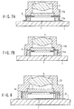
- FIGS. 7A and 7B shows further another modification of the present embodiment.
- FIGS. 7A and 7B are cross-sectional views in the directions perpendicular to each other.
- engagement between the lens holder 13b and the module board 1 is achieved at the position indicated in FIG. 7B.
- the engagement between the lens holder 13b and the module board 1 is not achieved.
- the surface of the lens holder 13b, which is opposed to the module board 1 has a width substantially equal to the width of the connector 12a and is not formed to extend to he side surface of the connector 12a as a connection part of the connector 12a (where an external lead terminal is formed).
- the surface of the lens holder 13, which is opposed to the module board 1 is formed to extend to the side surface of the connector 12a. This part is engaged with the connector 12a with the external terminal of the flexible board 8 set inside. In this manner, mechanical connection is achieved, and it is possible to attain electric connection between the external connection terminal 8b and the spring electrodes 15 of the connector 12a.
- FIG. 8 is a cross-sectional view showing the structure of a camera module according to further another modification of the present embodiment.
- a connector 23 made of conductive rubber is used in place of the connector 12 described above, and a photoelectric conversion module 6a is used in place of the connector 12.
- the external connection terminal of the photoelectric conversion module 6a is connected to the electrode pattern of the module board 1 through the connector 32.
- the connector 32 made of conductive rubber is formed by burying a spring made of brass material or the like subjected to plating processing of nickel and gold, as conductive material, in elastic silicone rubber. It is therefore possible to attain electric conductance with anisotropy by compressive deformation of the silicone rubber and spring.
- the connector 32 made of conductive rubber has a relatively high connection resistance (about several ten to several hundred m ⁇ ), it enables fine wiring at a pitch of 50 ⁇ m and downsizing to a width of about 1 mm.
- a conductive rubber connector 32 is provided between the lens holder 33 and the module board 1, to attain electric connection by a compression force between the lens holder 33 and the module board 1.
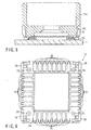
- FIG. 9 is a cross-sectional view showing the structure of a camera module integrated with a lens, which is incorporated in an image pickup apparatus according to a second embodiment of the present invention.
- the same functional parts as those of FIGS. 1 and 2 will be denoted at the same reference symbols, and detailed explanation thereof will be omitted herefrom.
- a signal processing IC 2 is mounted on one surface (front) of the module board 1 by means of flip-chip junction.
- the connector 12 and the chip components 3 are mounted on that surface of the board 1, too.
- a rubber sheet 35 covers the upper surface of the signal processing IC 2.
- a photoelectric transducer element 7 is provided on the rubber sheet 35.
- the lens holder 13 holds an optical lens 5.
- the lens holder 13 is fitted into the connector 12.
- the photoelectric module 6 is thereby clamped between the connector 12 and the lens holder 13.
- the lens holder 13 can be connected to the connector 12 while maintaining the optical distance between the optical lens 5 and the photoelectric conversion element 7.
- a connector 4 for connection to the main board is mounted by soldering.
- the chip component 3 is installed at a different position.
- the same advantages as those of the embodiment described above can be obtained, and the signal processing IC 2 and the photoelectric conversion module 6 are constructed in a layered structure through a rubber sheet 35, in the side of the front surface of the module board 1. Therefore, no dead space exists on the back surface of the module board 1, contributing to total downsizing.
- the degree of freedom increases when mounting a connector 4 and chip components 3 on the module board 1. Therefore, the entire apparatus can be formed to be very compact.
- the optical lens 13 can be connected to the connecter while maintaining the optical distance to the photoelectric conversion element due to compression deformation of the elastic material.
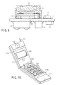
- FIG. 10 is a perspective view of a portable telephone (portable apparatus) according a third embodiment of this invention.
- the telephone incorporates an image pickup apparatus according to any one of the embodiments described above.
- the portable telephone apparatus comprises an image pickup device 111 and a display section 112, as an image transmission function, in addition to a general telephone function based on voices.
- the portable phone apparatus comprises two cases 114a and 114b which can be opened by a hinge 113.
- One case 114a is provided with an input microphone 115 and a keyboard 116.
- the other case 114b is provided with an antenna 117, a speaker 118, a liquid crystal display section 112, and an image pick up apparatus 111. Any of the image pickup apparatuses explained in the above embodiments is used for the image pickup apparatus 111.
- the photoelectric module is not directly connected to the module board. Rather, a connector electrically connects the module to the board. Hence, the apparatus can be manufactured, without performing a heating-process on the photoelectric module.
- the photoelectric module can attain high quality. Additionally, the components can be mounted on the module board at high density, successfully rendering the image pickup apparatus as small as desired.
- the electric apparatus that incorporates the image pickup apparatus can be have a simple internal structure. If any portable electric apparatus that incorporates the image pickup apparatus can be easily manufactured.
- FIGS. 11A and 11B show a camera module 200 integrated with a lens, which is incorporated in the image pickup apparatus according to a fourth embodiment of the present invention.
- FIG. 11A is a plan view showing a lens holder 210
- FIG. 11B is a plan view showing a connector 240.
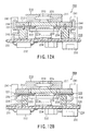
- FIGS. 12A and 12B are views showing cross-sections of the camera module 200.
- FIG. 12A is a cross-sectional view cut along the position of the line I-I' in FIG. 11B, observed in the arrow direction.
- FIG. 12B is a cross-sectional view cut along the line II-II' in FIG. 11B, observed in the arrow direction.
- the camera module 200 comprises a lens holder 210, a photoelectric conversion module 220, a module board 230, and a connector 240.
- the lens holder 210 comprises a cylindrical lens-barrel part 211 and a plate-like plug part 212 attached to this lens-barrel part 211.
- An optical lens 213 is attached to the lens-barrel part 211.
- An opening part is provided in the plug part 212 and is provided on the extended line of the optical axis of the optical lens 213.
- a flat part in the periphery of this opening is opposed to an area of the flexible board 221 that includes an external connection terminal, and is used for installation of a connector 240 which will be described later.
- the lens holder 210 may be provided with a diaphragm function.
- the photoelectric conversion module 220 comprises a flexible board 221.
- the flexible board 221 is formed of a base board made of polyimide and having a thickness of 25 ⁇ m, and a gold-plated copper wire is formed through an adhesive agent layer. On the back surface of the base board, a cover film layer having a thickness of about 200 ⁇ m is formed through an adhesive agent layer. So constructed, the flexible board 221 is rigid to some degree, preventing positional changes of the sensor. Note that the material of the flexible board 221 may be polyester, liquid crystal polymer, or the like in place of polyimide and is not limited hitherto.
- An opening part 221a is formed at the center of the flexible board 221.
- a bare chip of a photoelectric conversion element 222 such as a CCD, a CMOS sensor, or the like is installed, and the photoelectric conversion part of the photoelectric conversion element 222 is arranged so as to face the opening part 221a.
- This photoelectric conversion element 222 is mounted by flip chip assembly to the flexible board 221 through a bump (external connection terminal) 224 by an anisotropic conductive adhesive film 223.
- the bump electrode 226 of the flexible board 221 for example, total thirty terminals are arranged in two parallel rows at a pitch of about 0.5 mm.
- Optical glass 225 is fixed to the surface of this flexible board 221, by an adhesive agent, so as to face the opening part 221a and oppose to the photoelectric conversion element 222.
- On the surface of the optical glass 225 there is provided a thin film made of one layer or multiple layers, in correspondence with a required optical characteristic.
- an external connection terminal 226 like an electrode pad used for connection to the outside is formed at an outer circumferential part of the flexible board 221 in the side of its back surface.
- the apparatus can be assembled without applying much heat to the photoelectric conversion element 222. It is possible to make junction by flip chip bonding based on ultrasonic junction or by photosensitive resin.
- a bump 224 for connection, which is formed on the electrode pad of the photoelectric conversion element 222 is a gold ball having a diameter of several ten to hundred and several ten ⁇ m.
- the bump 224 is provided by electric plating, a wire bonding method, or a transfer method.
- the module board 230 comprises, for example, a double-sided wiring board 231 using a glass epoxy board (FR-4) subjected to multi-layer wiring of six layers, a ceramic board, a glass wiring board, or the like.
- FR-4 glass epoxy board
- chip components 232 and a connector 233 for external connection are mounted by soldering.
- a signal processing IC (DSP) 234 mounted by flip chip bonding, a connection part 235, and spring electrodes 236 soldered to the connection part 235 are provided.
- a connector 240 of a surface mount type is soldered to an electrode on the surface of the module board 230, by reflow soldering, and is thus mechanically fixed thereto.
- insertion guide posts 241 are provided respectively at four corners of the connector 240.
- the connector 240 has two positioning pins 242 and 243 that have different diameters.
- the positioning pins 242 and 243 are diametrically opposite to each other across the opening.
- the insertion guide posts 241 for placing the lens holder 210 and the module board 230 at desired positions.
- the pins 242 and 243 cooperate to prevent the operator to inset the lens holder 210 in a wrong direction.
- the connector 240 is provided with a lens holder fixing metal fitting 244 for fixing the lens holder 210, and a part of the fitting is mechanically fixed to the module board 230 by soldering.
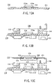
- FIGS. 13A to 13E are cross-sectional views cut along the position II'-I' and observed in the arrow direction.
- a signal processing IC 234 and the like are previously mounted by flip chip bonding through an anisotropic conductive adhesive film on the surface of a module board 230.
- a bump 234a is previously formed at an electrode of the signal processing IC 234.
- the anisotropic conductive adhesive film may be provided as a paste-like material by pattern-applying it a dispense method, a screen printing method, or the like or by adhering a sheet-like material.
- the anisotropic adhesive film has been made by kneading metal particles into thermosetting epoxy resin.
- the surface where the bump 234a is provided is pressed against the anisotropic conductive adhesive film (for about 10 seconds at 200°C) to achieve thermocompression bonding.
- the electrodes of the signal processing IC 234 and the module board are connected by the bump 234a, thereby to attain electric connection therebetween.
- the electrodes of the signal processing IC 234 and the module board 230 may be connected to each other.
- chip components 232 and an external connector 234 are mounted on the backside of the module board 230.
- the connector 240 is fastened to the module board 230 by means of re-flow soldering.
- the connector 240 surrounds the signal processing IC 234 mounted on the module board 230.
- the external connection terminal 226 of the flexible board 221 is arranged above the connector 240 so as to correspond to spring electrodes 236 of the connector 240, with use of positioning pins 242 and 243 and a positioning hole 211a, above the connector 240.
- the lens holder 210 which fixes and holds the optical lens 213 is inserted to be pressed against the spring electrodes of the connector 240 through the flexible board 221.
- the lens holder fixing metal fitting 244 spreads outward with an elastic force.
- the inside of the lens holder 210 is let contact the surface of the optical glass 225 of the photoelectric conversion module 220, the optical lens 213 and the photoelectric conversion element 222 are arranged so as to oppose each other while the optical distance therebetween is maintained at a predetermined value.
- the spring electrodes 236 are electrically connected to the electrodes on the surface of the module board 230 by soldering, and at the spring parts, the spring electrodes is pressed into contact with the external connection terminal 226, thereby to attain electric connection.
- the photoelectric conversion element 222 can be electrically connected very easily, in a short time, to the module board 230 to which the optical system having a lens, the chip components 232, and the like are reflow-connected, by mechanical press-contact between the plug part 212 of the lens holder 210 and the spring electrodes 236 of the connector 240. It is therefore possible to provide camera modules having a small size with excellent yield.
- a stack structure with the photoelectric conversion element 222 can be constructed by flip chip bonding the signal processing IC 234 at this area. Therefore, there is a high advantage in down-sizing of the module board area.
- stress can be prevented from being concentrated on the lens holder 210 and the lens holder fixing metal fitting 244, by providing the insertion guide posts 241 of the lens holder 210 at four corners of the connector 240 and by further arranging the outer shape thereof in the outside of the lens holder 210 and the lens holder fixing metal fitting 244.
- the structure is arranged such that a part of the outer circumference of the lens holder 210 is guided by the insertion guide posts 241 at the four corners when inserting the lens holder 210.
- the mechanism is constructed such that the lens holder can be simply and securely inserted can be even in case where an operator cannot directly observe the positioning pins 242 and 243. Therefore, the productivity can be improved.
- the outer sides of the insertion guide posts 241 are arranged outside any of the lens holder 210 and the lens holder fixing metal fitting 244. In this manner, for example, it is possible to avoid at least the stress being concentrated only on the lens holder fixing metal fitting 244 when interference with an external casing occurs at the time of drop impact, and to prevent image quality from being reduced due to a position shift of the optical lens 213.
- the image pickup apparatus according to the present embodiment may be incorporated in the portable phone apparatus shown in FIG. 10.
- a screw structure may be provided for both of a cylindrical bulk to which the optical lens 213 is attached and the lens-barrel of the lens holder, thereby to construct a positioning mechanism.
Landscapes
- Engineering & Computer Science (AREA)
- Multimedia (AREA)
- Signal Processing (AREA)
- Transforming Light Signals Into Electric Signals (AREA)
- Solid State Image Pick-Up Elements (AREA)
- Studio Devices (AREA)
Abstract
Description
Chip components or the like (not shown) forming part of a camera module must be mounted in the outside thereof, thereby limiting the downsizing.
Claims (9)
- An image pickup apparatus (200) characterized by comprising:a first connector (240) arranged on a wiring board (1) ;a second connector (210) including an optical lens (213) and being engageable with the first connector (240); anda photoelectric conversion module (220) on which light is incident from the optical lens (213), said photoelectric conversion module (220) being fixedly held when the photoelectric conversion module (220) is clamped by the first and second connectors (240, 210) in a state where the first and second connectors (240, 210) are in engagement and coupled relatively to each other.
- An image pickup apparatus (200) according to claim 1, characterized in that said photoelectric conversion module (220) comprises:a wiring board (221) including an opening (221a);a photoelectric conversion element (234) provided for one major surface of the wiring board (221) and including a photoelectric conversion surface that opposes the opening (221a); anda transparent member (225) provided for another major surface of the wiring board (221) and covering both the opening (221a) and the photoelectric conversion surface,
- An image pickup apparatus (200) according to any preceding claim, characterized by further comprising a spring electrode (236) electrically connected to a terminal of the photoelectric conversion element (234) and located at a position where the first connector (240) is in contact with the photoelectric conversion module (220), said spring electrode (236) being electrically connected to the wiring board (221).
- An image pickup apparatus (200) according to any preceding claim, characterized in that said second connector (210) includes a lens barrel (211).
- An image pickup apparatus (200) according to any of claims 1 to 3, characterized in that said second connector includes a lens barrel, and said lens barrel (211) has at least one opening which opposes the optical lens (213) and which is provided with a diaphragm.
- An image pickup apparatus (200) according to any preceding claim, characterized in that said first connector (240) includes a guide (241) which guides the second connector (210) to a predetermined position.
- An image pickup apparatus (200) according to any preceding claim, characterized in that said first connector (240) includes an elastic member (244) which urges the second connector (210) toward the first connector 240 when the first and second connectors (240, 210) are brought into engagement and coupled relatively to each other.
- A method for manufacturing an image pickup apparatus (200), characterized by comprising:an installation step of arranging a first connector (240) and an electronic component (232) on a wiring board (230) and electrically connecting the first connector (240) and the electronic component (232) together; andan assembly step of electrically connecting an electrode of the first connector (240) to a second connector (210) including an optical lens (213), when the first connector (240) and the second connector (210) are brought into engagement, said assembly step being executed by inserting a photoelectric conversion module (220), including a photoelectric conversion element (234) on which light from the optical lens (213) of the second connector (210) is incident, between the first connector (240) and the second connector (210).
- A portable electronic apparatus comprising the image pickup apparatus defined in any one of claims 1 through 7.
Applications Claiming Priority (2)
| Application Number | Priority Date | Filing Date | Title |
|---|---|---|---|
| JP2000346564 | 2000-11-14 | ||
| JP2000346564 | 2000-11-14 |
Publications (4)
| Publication Number | Publication Date |
|---|---|
| EP1220324A2 true EP1220324A2 (en) | 2002-07-03 |
| EP1220324A3 EP1220324A3 (en) | 2003-10-29 |
| EP1220324B1 EP1220324B1 (en) | 2009-02-18 |
| EP1220324B8 EP1220324B8 (en) | 2009-04-22 |
Family
ID=18820413
Family Applications (1)
| Application Number | Title | Priority Date | Filing Date |
|---|---|---|---|
| EP01309617A Expired - Lifetime EP1220324B8 (en) | 2000-11-14 | 2001-11-14 | Image pickup apparatus, method of manufacturing, and electric apparatus |
Country Status (5)
| Country | Link |
|---|---|
| US (1) | US7304684B2 (en) |
| EP (1) | EP1220324B8 (en) |
| CN (1) | CN1157052C (en) |
| DE (1) | DE60137676D1 (en) |
| TW (1) | TW528889B (en) |
Cited By (8)
| Publication number | Priority date | Publication date | Assignee | Title |
|---|---|---|---|---|
| FR2854498A1 (en) * | 2003-04-29 | 2004-11-05 | St Microelectronics Sa | SEMICONDUCTOR PACKAGE WITH OPTICAL SENSOR MOUNTING INSIDE AN OBJECT. |
| FR2861217A1 (en) * | 2003-10-21 | 2005-04-22 | St Microelectronics Sa | OPTICAL DEVICE FOR OPTICAL SEMICONDUCTOR HOUSING AND METHOD OF MANUFACTURING THE SAME |
| DE10344768B3 (en) * | 2003-09-26 | 2005-08-18 | Siemens Ag | Optical module with resilient element between lens holder and circuit carrier and optical system |
| FR2869158A1 (en) * | 2004-04-20 | 2005-10-21 | St Microelectronics Sa | OPTICAL SEMICONDUCTOR HOUSING WITH MEDIUM COMPRESSIBLE ADJUSTMENT |
| DE102006005519A1 (en) * | 2006-02-07 | 2007-08-09 | Siemens Ag | Optical detection system |
| DE102006035635A1 (en) * | 2006-07-31 | 2008-02-07 | Osram Opto Semiconductors Gmbh | lighting arrangement |
| EP2112538A1 (en) * | 2008-04-25 | 2009-10-28 | Hitachi, Ltd. | Camera unit |
| DE102013223858A1 (en) * | 2013-11-21 | 2015-05-21 | Conti Temic Microelectronic Gmbh | Optical device with optical module, image pickup element and carrier plate |
Families Citing this family (117)
| Publication number | Priority date | Publication date | Assignee | Title |
|---|---|---|---|---|
| WO2003103014A2 (en) | 2002-05-30 | 2003-12-11 | Koninklijke Philips Electronics N.V. | Electronic imaging device |
| JP2004104078A (en) * | 2002-06-28 | 2004-04-02 | Sanyo Electric Co Ltd | Camera module and manufacturing method thereof |
| CN100380924C (en) * | 2002-07-18 | 2008-04-09 | 皇家飞利浦电子股份有限公司 | Camera module, holder for use in camera module, camera system and method of manufacturing camera module |
| JP2005533451A (en) * | 2002-07-18 | 2005-11-04 | コーニンクレッカ フィリップス エレクトロニクス エヌ ヴィ | Camera module, holder used in camera module, camera system, and method of manufacturing camera module |
| US6823582B1 (en) * | 2002-08-02 | 2004-11-30 | National Semiconductor Corporation | Apparatus and method for force mounting semiconductor packages to printed circuit boards |
| JP2004103860A (en) | 2002-09-10 | 2004-04-02 | Fujitsu Ltd | Semiconductor device, camera module and method of manufacturing the same |
| TW558064U (en) * | 2002-09-23 | 2003-10-11 | Ist Internat Semiconductor Tec | Thin type camera module |
| JP5030360B2 (en) * | 2002-12-25 | 2012-09-19 | オリンパス株式会社 | Method for manufacturing solid-state imaging device |
| FI20030071L (en) * | 2003-01-17 | 2004-07-18 | Nokia Corp | Placing the camera module in a portable device |
| JP4204368B2 (en) * | 2003-03-28 | 2009-01-07 | シャープ株式会社 | Optical device module and method of manufacturing optical device module |
| JP2004304604A (en) * | 2003-03-31 | 2004-10-28 | Mitsumi Electric Co Ltd | Mounting structure of small camera module to socket |
| FR2854496B1 (en) * | 2003-04-29 | 2005-09-16 | St Microelectronics Sa | SEMICONDUCTOR HOUSING |
| TW579169U (en) * | 2003-05-28 | 2004-03-01 | Benq Corp | Optical module for a digital camera |
| KR100526191B1 (en) * | 2003-06-18 | 2005-11-03 | 삼성전자주식회사 | Solid-State Imaging Apparatus |
| TWM244685U (en) * | 2003-07-04 | 2004-09-21 | Hon Hai Prec Ind Co Ltd | Digital cameral module |
| US6934065B2 (en) * | 2003-09-18 | 2005-08-23 | Micron Technology, Inc. | Microelectronic devices and methods for packaging microelectronic devices |
| US7091124B2 (en) | 2003-11-13 | 2006-08-15 | Micron Technology, Inc. | Methods for forming vias in microelectronic devices, and methods for packaging microelectronic devices |
| US8084866B2 (en) | 2003-12-10 | 2011-12-27 | Micron Technology, Inc. | Microelectronic devices and methods for filling vias in microelectronic devices |
| US7583862B2 (en) * | 2003-11-26 | 2009-09-01 | Aptina Imaging Corporation | Packaged microelectronic imagers and methods of packaging microelectronic imagers |
| JP3921467B2 (en) * | 2003-12-11 | 2007-05-30 | シャープ株式会社 | CAMERA MODULE, CAMERA MODULE MANUFACTURING METHOD, ELECTRONIC DEVICE, AND ELECTRONIC DEVICE MANUFACTURING METHOD |
| US7253397B2 (en) * | 2004-02-23 | 2007-08-07 | Micron Technology, Inc. | Packaged microelectronic imagers and methods of packaging microelectronic imagers |
| KR100593555B1 (en) * | 2004-02-26 | 2006-06-28 | (주)아이디에스 | Video camera module |
| US7663693B2 (en) * | 2004-03-01 | 2010-02-16 | United Microelectronics Corp. | Camera module |
| TWI282873B (en) * | 2004-03-12 | 2007-06-21 | Premier Image Technology Corp | Lens module and assembling method thereof |
| JP4446773B2 (en) * | 2004-03-26 | 2010-04-07 | 富士フイルム株式会社 | Imaging device |
| JP2005284147A (en) * | 2004-03-30 | 2005-10-13 | Fuji Photo Film Co Ltd | Imaging device |
| US7632713B2 (en) * | 2004-04-27 | 2009-12-15 | Aptina Imaging Corporation | Methods of packaging microelectronic imaging devices |
| US7368695B2 (en) * | 2004-05-03 | 2008-05-06 | Tessera, Inc. | Image sensor package and fabrication method |
| US20060109366A1 (en) * | 2004-05-04 | 2006-05-25 | Tessera, Inc. | Compact lens turret assembly |
| CN1969539A (en) * | 2004-05-04 | 2007-05-23 | 德塞拉股份有限公司 | Compact lens turret assembly |
| US20050247894A1 (en) | 2004-05-05 | 2005-11-10 | Watkins Charles M | Systems and methods for forming apertures in microfeature workpieces |
| JP3830495B2 (en) * | 2004-05-10 | 2006-10-04 | シャープ株式会社 | Semiconductor device, semiconductor device manufacturing method, and optical device module |
| US7253957B2 (en) * | 2004-05-13 | 2007-08-07 | Micron Technology, Inc. | Integrated optics units and methods of manufacturing integrated optics units for use with microelectronic imagers |
| US8092734B2 (en) * | 2004-05-13 | 2012-01-10 | Aptina Imaging Corporation | Covers for microelectronic imagers and methods for wafer-level packaging of microelectronics imagers |
| US20050275750A1 (en) | 2004-06-09 | 2005-12-15 | Salman Akram | Wafer-level packaged microelectronic imagers and processes for wafer-level packaging |
| US7498647B2 (en) | 2004-06-10 | 2009-03-03 | Micron Technology, Inc. | Packaged microelectronic imagers and methods of packaging microelectronic imagers |
| US7262405B2 (en) * | 2004-06-14 | 2007-08-28 | Micron Technology, Inc. | Prefabricated housings for microelectronic imagers |
| US7199439B2 (en) * | 2004-06-14 | 2007-04-03 | Micron Technology, Inc. | Microelectronic imagers and methods of packaging microelectronic imagers |
| US7714931B2 (en) * | 2004-06-25 | 2010-05-11 | Flextronics International Usa, Inc. | System and method for mounting an image capture device on a flexible substrate |
| US7294897B2 (en) * | 2004-06-29 | 2007-11-13 | Micron Technology, Inc. | Packaged microelectronic imagers and methods of packaging microelectronic imagers |
| US7232754B2 (en) * | 2004-06-29 | 2007-06-19 | Micron Technology, Inc. | Microelectronic devices and methods for forming interconnects in microelectronic devices |
| US7416913B2 (en) * | 2004-07-16 | 2008-08-26 | Micron Technology, Inc. | Methods of manufacturing microelectronic imaging units with discrete standoffs |
| US7189954B2 (en) * | 2004-07-19 | 2007-03-13 | Micron Technology, Inc. | Microelectronic imagers with optical devices and methods of manufacturing such microelectronic imagers |
| US7402453B2 (en) * | 2004-07-28 | 2008-07-22 | Micron Technology, Inc. | Microelectronic imaging units and methods of manufacturing microelectronic imaging units |
| US20060023107A1 (en) * | 2004-08-02 | 2006-02-02 | Bolken Todd O | Microelectronic imagers with optics supports having threadless interfaces and methods for manufacturing such microelectronic imagers |
| US7364934B2 (en) | 2004-08-10 | 2008-04-29 | Micron Technology, Inc. | Microelectronic imaging units and methods of manufacturing microelectronic imaging units |
| US7223626B2 (en) * | 2004-08-19 | 2007-05-29 | Micron Technology, Inc. | Spacers for packaged microelectronic imagers and methods of making and using spacers for wafer-level packaging of imagers |
| US7397066B2 (en) * | 2004-08-19 | 2008-07-08 | Micron Technology, Inc. | Microelectronic imagers with curved image sensors and methods for manufacturing microelectronic imagers |
| US7429494B2 (en) * | 2004-08-24 | 2008-09-30 | Micron Technology, Inc. | Microelectronic imagers with optical devices having integral reference features and methods for manufacturing such microelectronic imagers |
| US7115961B2 (en) * | 2004-08-24 | 2006-10-03 | Micron Technology, Inc. | Packaged microelectronic imaging devices and methods of packaging microelectronic imaging devices |
| US7425499B2 (en) | 2004-08-24 | 2008-09-16 | Micron Technology, Inc. | Methods for forming interconnects in vias and microelectronic workpieces including such interconnects |
| US7276393B2 (en) | 2004-08-26 | 2007-10-02 | Micron Technology, Inc. | Microelectronic imaging units and methods of manufacturing microelectronic imaging units |
| US7083425B2 (en) | 2004-08-27 | 2006-08-01 | Micron Technology, Inc. | Slanted vias for electrical circuits on circuit boards and other substrates |
| US7511262B2 (en) * | 2004-08-30 | 2009-03-31 | Micron Technology, Inc. | Optical device and assembly for use with imaging dies, and wafer-label imager assembly |
| US20070148807A1 (en) * | 2005-08-22 | 2007-06-28 | Salman Akram | Microelectronic imagers with integrated optical devices and methods for manufacturing such microelectronic imagers |
| US7646075B2 (en) * | 2004-08-31 | 2010-01-12 | Micron Technology, Inc. | Microelectronic imagers having front side contacts |
| US7300857B2 (en) | 2004-09-02 | 2007-11-27 | Micron Technology, Inc. | Through-wafer interconnects for photoimager and memory wafers |
| US7294827B2 (en) * | 2004-09-21 | 2007-11-13 | Delphi Technologies, Inc. | Electronic module with light-blocking features |
| US7271482B2 (en) * | 2004-12-30 | 2007-09-18 | Micron Technology, Inc. | Methods for forming interconnects in microelectronic workpieces and microelectronic workpieces formed using such methods |
| US7214919B2 (en) * | 2005-02-08 | 2007-05-08 | Micron Technology, Inc. | Microelectronic imaging units and methods of manufacturing microelectronic imaging units |
| US7303931B2 (en) * | 2005-02-10 | 2007-12-04 | Micron Technology, Inc. | Microfeature workpieces having microlenses and methods of forming microlenses on microfeature workpieces |
| US20060177999A1 (en) * | 2005-02-10 | 2006-08-10 | Micron Technology, Inc. | Microelectronic workpieces and methods for forming interconnects in microelectronic workpieces |
| US7190039B2 (en) * | 2005-02-18 | 2007-03-13 | Micron Technology, Inc. | Microelectronic imagers with shaped image sensors and methods for manufacturing microelectronic imagers |
| WO2006106953A1 (en) * | 2005-04-01 | 2006-10-12 | Matsushita Electric Industrial Co., Ltd. | Image pickup device |
| DE102005022406A1 (en) * | 2005-05-13 | 2006-11-23 | Robert Bosch Gmbh | Image sensor recording system and method of manufacture |
| EP1734743A3 (en) * | 2005-06-16 | 2011-08-31 | Basler Aktiengesellschaft | Carrier for sensor boards |
| CN1885909A (en) * | 2005-06-24 | 2006-12-27 | 鸿富锦精密工业(深圳)有限公司 | Digital camera module |
| US7795134B2 (en) | 2005-06-28 | 2010-09-14 | Micron Technology, Inc. | Conductive interconnect structures and formation methods using supercritical fluids |
| US20060290001A1 (en) * | 2005-06-28 | 2006-12-28 | Micron Technology, Inc. | Interconnect vias and associated methods of formation |
| US7288757B2 (en) * | 2005-09-01 | 2007-10-30 | Micron Technology, Inc. | Microelectronic imaging devices and associated methods for attaching transmissive elements |
| US7622377B2 (en) | 2005-09-01 | 2009-11-24 | Micron Technology, Inc. | Microfeature workpiece substrates having through-substrate vias, and associated methods of formation |
| US7262134B2 (en) | 2005-09-01 | 2007-08-28 | Micron Technology, Inc. | Microfeature workpieces and methods for forming interconnects in microfeature workpieces |
| US7863187B2 (en) | 2005-09-01 | 2011-01-04 | Micron Technology, Inc. | Microfeature workpieces and methods for forming interconnects in microfeature workpieces |
| JP4618507B2 (en) | 2005-10-28 | 2011-01-26 | ソニー株式会社 | Camera module and electronic equipment |
| KR100748722B1 (en) * | 2006-04-03 | 2007-08-13 | 삼성전자주식회사 | Micro Device Package Module and Manufacturing Method Thereof |
| DE102006019717A1 (en) * | 2006-04-27 | 2007-10-31 | Siemens Ag | Optical module, has snap-in hook arranged in such a manner that surface of printed circuit board is aligned at definite preset distance with respect to optical lens in self adjustable manner |
| US7749899B2 (en) | 2006-06-01 | 2010-07-06 | Micron Technology, Inc. | Microelectronic workpieces and methods and systems for forming interconnects in microelectronic workpieces |
| US7629249B2 (en) | 2006-08-28 | 2009-12-08 | Micron Technology, Inc. | Microfeature workpieces having conductive interconnect structures formed by chemically reactive processes, and associated systems and methods |
| WO2008027576A1 (en) | 2006-08-31 | 2008-03-06 | Flextronics Ap, Llc | Discreetly positionable camera housing |
| US7902643B2 (en) | 2006-08-31 | 2011-03-08 | Micron Technology, Inc. | Microfeature workpieces having interconnects and conductive backplanes, and associated systems and methods |
| CN101141562A (en) * | 2006-09-08 | 2008-03-12 | 鸿富锦精密工业(深圳)有限公司 | Image sensing device |
| TWI394432B (en) * | 2006-11-27 | 2013-04-21 | Hon Hai Prec Ind Co Ltd | Digital camera modules and method of manufacturing the same |
| JP2008148222A (en) * | 2006-12-13 | 2008-06-26 | Matsushita Electric Ind Co Ltd | Solid-state imaging device and manufacturing method thereof |
| US7593636B2 (en) * | 2007-02-01 | 2009-09-22 | Tessera, Inc. | Pin referenced image sensor to reduce tilt in a camera module |
| JP4302745B2 (en) * | 2007-02-19 | 2009-07-29 | シャープ株式会社 | CAMERA DEVICE AND ELECTRONIC DEVICE HAVING THE SAME |
| CN101303444A (en) * | 2007-05-11 | 2008-11-12 | 鸿富锦精密工业(深圳)有限公司 | Camera module and assembly method thereof |
| CN101303443A (en) * | 2007-05-11 | 2008-11-12 | 鸿富锦精密工业(深圳)有限公司 | Camera module and assembly method thereof |
| JP2009017234A (en) * | 2007-07-04 | 2009-01-22 | Sharp Corp | Camera device |
| SG150410A1 (en) | 2007-08-31 | 2009-03-30 | Micron Technology Inc | Partitioned through-layer via and associated systems and methods |
| JP2009086075A (en) * | 2007-09-28 | 2009-04-23 | Alps Electric Co Ltd | Lens with lens barrel |
| CN102313959B (en) * | 2007-11-21 | 2014-11-12 | Lg伊诺特有限公司 | Camera module |
| US7884015B2 (en) | 2007-12-06 | 2011-02-08 | Micron Technology, Inc. | Methods for forming interconnects in microelectronic workpieces and microelectronic workpieces formed using such methods |
| US20100194465A1 (en) * | 2009-02-02 | 2010-08-05 | Ali Salih | Temperature compensated current source and method therefor |
| KR101594831B1 (en) * | 2009-03-26 | 2016-02-17 | 삼성전자 주식회사 | Structure for fixing camera module on bio drive |
| KR20110001659A (en) * | 2009-06-30 | 2011-01-06 | 삼성테크윈 주식회사 | Camera module |
| CN101998035B (en) * | 2009-08-24 | 2013-07-03 | 鸿富锦精密工业(深圳)有限公司 | Camera module and assembling method thereof |
| TW201210326A (en) * | 2010-08-19 | 2012-03-01 | Hon Hai Prec Ind Co Ltd | Camera module and manufacturing method of the same |
| TW201210327A (en) * | 2010-08-19 | 2012-03-01 | Hon Hai Prec Ind Co Ltd | Camera module and manufacturing method of the same |
| TWI483026B (en) * | 2011-01-10 | 2015-05-01 | Hon Hai Prec Ind Co Ltd | Camera module |
| US8982267B2 (en) | 2011-07-27 | 2015-03-17 | Flextronics Ap, Llc | Camera module with particle trap |
| US9136289B2 (en) * | 2011-08-23 | 2015-09-15 | Flextronics Ap, Llc | Camera module housing having built-in conductive traces to accommodate stacked dies using flip chip connections |
| EP3627553B1 (en) * | 2012-02-07 | 2022-07-20 | Nikon Corporation | Imaging unit and imaging apparatus |
| JP6131952B2 (en) * | 2012-07-20 | 2017-05-24 | 株式会社ニコン | Imaging unit, imaging apparatus, and manufacturing method of imaging unit |
| KR102089445B1 (en) * | 2012-08-08 | 2020-03-17 | 엘지이노텍 주식회사 | Camera Module |
| US9060111B2 (en) * | 2012-09-06 | 2015-06-16 | Apple Inc. | Electronic device with compact camera module |
| CN111432106B (en) * | 2013-12-27 | 2022-05-13 | 株式会社尼康 | Imaging unit and imaging device |
| CN104954634B (en) * | 2014-03-25 | 2019-01-29 | 宁波舜宇光电信息有限公司 | A kind of camera module and its manufacturing method |
| US9691801B2 (en) * | 2014-12-22 | 2017-06-27 | Stmicroelectronics Pte Ltd | Image sensing device with cap and related methods |
| EP4488751B1 (en) | 2015-06-08 | 2026-01-28 | LG Innotek Co., Ltd. | Camera module |
| CN105450913B (en) * | 2015-12-01 | 2020-04-28 | 宁波舜宇光电信息有限公司 | Camera module, electric bracket, assembling method and application thereof |
| US10750071B2 (en) * | 2016-03-12 | 2020-08-18 | Ningbo Sunny Opotech Co., Ltd. | Camera module with lens array arrangement, circuit board assembly, and image sensor and manufacturing method thereof |
| US20190258019A1 (en) * | 2016-09-28 | 2019-08-22 | Sharp Kabushiki Kaisha | Optical apparatus and camera module |
| CN207781947U (en) * | 2017-03-10 | 2018-08-28 | 唐虞企业股份有限公司 | Connector with a locking member |
| CN107477184B (en) * | 2017-06-16 | 2023-10-13 | Oppo广东移动通信有限公司 | Seals, camera components, mobile terminals and installation methods of their cameras |
| CN111405145B (en) * | 2019-01-02 | 2021-12-07 | 三赢科技(深圳)有限公司 | Camera module and electronic device with same |
| JP6901603B1 (en) * | 2020-03-27 | 2021-07-14 | 日本航空電子工業株式会社 | Board-to-board connector |
| CN119730431A (en) * | 2025-02-27 | 2025-03-28 | 甬矽半导体(宁波)有限公司 | Image sensor packaging structure and preparation method thereof |
Family Cites Families (16)
| Publication number | Priority date | Publication date | Assignee | Title |
|---|---|---|---|---|
| US5191224A (en) * | 1987-04-22 | 1993-03-02 | Hitachi, Ltd. | Wafer scale of full wafer memory system, packaging method thereof, and wafer processing method employed therein |
| JP2605174B2 (en) * | 1989-11-30 | 1997-04-30 | 富士写真フイルム株式会社 | Mounting structure of solid-state imaging device |
| JP3035784B2 (en) * | 1990-01-09 | 2000-04-24 | コニカ株式会社 | Image recording device |
| JPH05275201A (en) * | 1992-03-27 | 1993-10-22 | Nec Corp | Connection terminal |
| JP3207319B2 (en) | 1993-05-28 | 2001-09-10 | 株式会社東芝 | Photoelectric conversion device and method of manufacturing the same |
| JP3355881B2 (en) | 1994-09-21 | 2002-12-09 | ソニー株式会社 | Solid-state imaging device and manufacturing method thereof |
| US5861654A (en) * | 1995-11-28 | 1999-01-19 | Eastman Kodak Company | Image sensor assembly |
| JP3138191B2 (en) * | 1995-08-10 | 2001-02-26 | 三洋電機株式会社 | Solid-state imaging device |
| US6795120B2 (en) * | 1996-05-17 | 2004-09-21 | Sony Corporation | Solid-state imaging apparatus and camera using the same |
| JPH10321827A (en) * | 1997-05-16 | 1998-12-04 | Sony Corp | Imaging device and camera |
| US6654064B2 (en) * | 1997-05-23 | 2003-11-25 | Canon Kabushiki Kaisha | Image pickup device incorporating a position defining member |
| JP3750276B2 (en) * | 1997-05-23 | 2006-03-01 | ソニー株式会社 | Method for mounting solid-state image sensor and method for mounting solid-state image sensor package |
| JP3836235B2 (en) * | 1997-12-25 | 2006-10-25 | 松下電器産業株式会社 | Solid-state imaging device and manufacturing method thereof |
| JP4003991B2 (en) * | 1998-04-14 | 2007-11-07 | Cbc株式会社 | Electronic imaging device |
| JP2000069336A (en) | 1998-08-26 | 2000-03-03 | Sanyo Electric Co Ltd | Mount structure for image pickup device |
| JP2001188155A (en) | 1999-12-28 | 2001-07-10 | Kuurii Components Kk | Image sensor fixing means |
-
2001
- 2001-11-13 US US09/986,909 patent/US7304684B2/en not_active Expired - Lifetime
- 2001-11-13 TW TW090128147A patent/TW528889B/en not_active IP Right Cessation
- 2001-11-14 DE DE60137676T patent/DE60137676D1/en not_active Expired - Lifetime
- 2001-11-14 CN CNB011436018A patent/CN1157052C/en not_active Expired - Fee Related
- 2001-11-14 EP EP01309617A patent/EP1220324B8/en not_active Expired - Lifetime
Cited By (17)
| Publication number | Priority date | Publication date | Assignee | Title |
|---|---|---|---|---|
| US7084473B2 (en) | 2003-04-29 | 2006-08-01 | Stmicroelectronics S.A. | Semiconductor package with an optical sensor which may be fit inside an object |
| FR2854498A1 (en) * | 2003-04-29 | 2004-11-05 | St Microelectronics Sa | SEMICONDUCTOR PACKAGE WITH OPTICAL SENSOR MOUNTING INSIDE AN OBJECT. |
| DE10344768B3 (en) * | 2003-09-26 | 2005-08-18 | Siemens Ag | Optical module with resilient element between lens holder and circuit carrier and optical system |
| US7268957B2 (en) | 2003-09-26 | 2007-09-11 | Siemens Aktiengesellschaft | Optical module and optical system |
| FR2861217A1 (en) * | 2003-10-21 | 2005-04-22 | St Microelectronics Sa | OPTICAL DEVICE FOR OPTICAL SEMICONDUCTOR HOUSING AND METHOD OF MANUFACTURING THE SAME |
| US7245834B2 (en) | 2003-10-21 | 2007-07-17 | Stmicroelectronics S.A. | Optical device for optical semiconductor package and fabrication method |
| US7504666B2 (en) | 2004-04-20 | 2009-03-17 | Stmicroelectronics S.A. | Optical semiconductor package with compressible adjustment means |
| FR2869158A1 (en) * | 2004-04-20 | 2005-10-21 | St Microelectronics Sa | OPTICAL SEMICONDUCTOR HOUSING WITH MEDIUM COMPRESSIBLE ADJUSTMENT |
| EP1589587A1 (en) * | 2004-04-20 | 2005-10-26 | Stmicroelectronics SA | Package for optical semiconductor with compressible control means |
| US7687819B2 (en) | 2004-04-20 | 2010-03-30 | Stmicroelectronics S.A. | Optical semiconductor package with compressible adjustment means |
| WO2007090694A1 (en) * | 2006-02-07 | 2007-08-16 | Continental Automotive Gmbh | Optical detection system |
| DE102006005519A1 (en) * | 2006-02-07 | 2007-08-09 | Siemens Ag | Optical detection system |
| DE102006035635A1 (en) * | 2006-07-31 | 2008-02-07 | Osram Opto Semiconductors Gmbh | lighting arrangement |
| US8585252B2 (en) | 2006-07-31 | 2013-11-19 | Osram Opto Semiconductors Gmbh | Lighting assembly |
| EP2112538A1 (en) * | 2008-04-25 | 2009-10-28 | Hitachi, Ltd. | Camera unit |
| US8005355B2 (en) | 2008-04-25 | 2011-08-23 | Hitachi, Ltd. | Camera unit |
| DE102013223858A1 (en) * | 2013-11-21 | 2015-05-21 | Conti Temic Microelectronic Gmbh | Optical device with optical module, image pickup element and carrier plate |
Also Published As
| Publication number | Publication date |
|---|---|
| TW528889B (en) | 2003-04-21 |
| CN1157052C (en) | 2004-07-07 |
| CN1354596A (en) | 2002-06-19 |
| US7304684B2 (en) | 2007-12-04 |
| EP1220324A3 (en) | 2003-10-29 |
| US20020057468A1 (en) | 2002-05-16 |
| EP1220324B1 (en) | 2009-02-18 |
| DE60137676D1 (en) | 2009-04-02 |
| EP1220324B8 (en) | 2009-04-22 |
Similar Documents
| Publication | Publication Date | Title |
|---|---|---|
| EP1220324B1 (en) | Image pickup apparatus, method of manufacturing, and electric apparatus | |
| JP2002223378A (en) | Imaging device, method of manufacturing the same, and electric device | |
| KR101008447B1 (en) | Camera module | |
| CN100484200C (en) | Camera assembly package | |
| CN1599428B (en) | Small Imaging Components | |
| US8714843B2 (en) | Camera module and method of manufacturing the same | |
| US7375757B1 (en) | Imaging element, imaging device, camera module and camera system | |
| EP1774453B1 (en) | System and method for mounting an image capture device on a flexible substrate | |
| KR20070068607A (en) | Camera module package | |
| CN101937923A (en) | shooting module | |
| CN112770019B (en) | Photosensitive assembly, preparation method thereof and camera module | |
| CN107155048A (en) | Dual camera module and terminal equipment | |
| JPWO2006088051A1 (en) | The camera module | |
| CN205407979U (en) | Dual camera module and terminal equipment | |
| CN115473988B (en) | Camera module and electronic equipment | |
| US10999683B2 (en) | Microphone assembly and electronic device comprising a microphone assembly | |
| KR100647015B1 (en) | LED housing structure and camera module package | |
| KR100832635B1 (en) | Multi camera module | |
| KR101393925B1 (en) | Camera Module | |
| KR100816843B1 (en) | Printed circuit board | |
| KR100716788B1 (en) | Substrate for image sensor module and image sensor module using same | |
| JP4000638B2 (en) | Burn-in socket | |
| JP2002314856A (en) | Camera for portable equipment | |
| KR101641527B1 (en) | Chip package for sensor, camera module including the chip package and method of manufacturing the chip package | |
| KR100640513B1 (en) | Substrate for image sensor module and image sensor module using same |
Legal Events
| Date | Code | Title | Description |
|---|---|---|---|
| PUAI | Public reference made under article 153(3) epc to a published international application that has entered the european phase |
Free format text: ORIGINAL CODE: 0009012 |
|
| 17P | Request for examination filed |
Effective date: 20011126 |
|
| AK | Designated contracting states |
Kind code of ref document: A2 Designated state(s): AT BE CH CY DE DK ES FI FR GB GR IE IT LI LU MC NL PT SE TR |
|
| AX | Request for extension of the european patent |
Free format text: AL;LT;LV;MK;RO;SI |
|
| PUAL | Search report despatched |
Free format text: ORIGINAL CODE: 0009013 |
|
| AK | Designated contracting states |
Kind code of ref document: A3 Designated state(s): AT BE CH CY DE DK ES FI FR GB GR IE IT LI LU MC NL PT SE TR |
|
| AX | Request for extension of the european patent |
Extension state: AL LT LV MK RO SI |
|
| AKX | Designation fees paid |
Designated state(s): DE FI FR GB |
|
| GRAP | Despatch of communication of intention to grant a patent |
Free format text: ORIGINAL CODE: EPIDOSNIGR1 |
|
| GRAS | Grant fee paid |
Free format text: ORIGINAL CODE: EPIDOSNIGR3 |
|
| GRAA | (expected) grant |
Free format text: ORIGINAL CODE: 0009210 |
|
| AK | Designated contracting states |
Kind code of ref document: B1 Designated state(s): DE FI FR GB |
|
| REG | Reference to a national code |
Ref country code: GB Ref legal event code: FG4D |
|
| RIN2 | Information on inventor provided after grant (corrected) |
Inventor name: ASAGA,JUNKABUSHIKI KAISHA TOSHIBA Inventor name: KARASAWA,JUNKABUSHIKI KAISHA TOSHIBA, Inventor name: SAGAWA, MASAO,KABUSHIKI KAISHA TOSHIBA Inventor name: OOISHI,MICHIKOKABUSHIKI KAISHA TOSHIBA, Inventor name: SASAKI, TOMOYUKIKABUSHIKI KAISHA TOSHIBA, |
|
| REF | Corresponds to: |
Ref document number: 60137676 Country of ref document: DE Date of ref document: 20090402 Kind code of ref document: P |
|
| PLBE | No opposition filed within time limit |
Free format text: ORIGINAL CODE: 0009261 |
|
| PLAA | Information modified related to event that no opposition was filed |
Free format text: ORIGINAL CODE: 0009299DELT |
|
| 26N | No opposition filed |
Effective date: 20091119 |
|
| PLBE | No opposition filed within time limit |
Free format text: ORIGINAL CODE: 0009261 |
|
| STAA | Information on the status of an ep patent application or granted ep patent |
Free format text: STATUS: NO OPPOSITION FILED WITHIN TIME LIMIT |
|
| D26N | No opposition filed (deleted) | ||
| 26N | No opposition filed |
Effective date: 20091119 |
|
| REG | Reference to a national code |
Ref country code: FR Ref legal event code: PLFP Year of fee payment: 15 |
|
| REG | Reference to a national code |
Ref country code: FR Ref legal event code: PLFP Year of fee payment: 16 |
|
| REG | Reference to a national code |
Ref country code: FR Ref legal event code: PLFP Year of fee payment: 17 |
|
| REG | Reference to a national code |
Ref country code: FR Ref legal event code: PLFP Year of fee payment: 18 |
|
| PGFP | Annual fee paid to national office [announced via postgrant information from national office to epo] |
Ref country code: DE Payment date: 20191029 Year of fee payment: 19 Ref country code: FI Payment date: 20191111 Year of fee payment: 19 |
|
| PGFP | Annual fee paid to national office [announced via postgrant information from national office to epo] |
Ref country code: FR Payment date: 20191014 Year of fee payment: 19 |
|
| PGFP | Annual fee paid to national office [announced via postgrant information from national office to epo] |
Ref country code: GB Payment date: 20191115 Year of fee payment: 19 |
|
| REG | Reference to a national code |
Ref country code: DE Ref legal event code: R119 Ref document number: 60137676 Country of ref document: DE |
|
| REG | Reference to a national code |
Ref country code: FI Ref legal event code: MAE |
|
| GBPC | Gb: european patent ceased through non-payment of renewal fee |
Effective date: 20201114 |
|
| PG25 | Lapsed in a contracting state [announced via postgrant information from national office to epo] |
Ref country code: FI Free format text: LAPSE BECAUSE OF NON-PAYMENT OF DUE FEES Effective date: 20201114 |
|
| PG25 | Lapsed in a contracting state [announced via postgrant information from national office to epo] |
Ref country code: FR Free format text: LAPSE BECAUSE OF NON-PAYMENT OF DUE FEES Effective date: 20201130 |
|
| PG25 | Lapsed in a contracting state [announced via postgrant information from national office to epo] |
Ref country code: DE Free format text: LAPSE BECAUSE OF NON-PAYMENT OF DUE FEES Effective date: 20210601 Ref country code: GB Free format text: LAPSE BECAUSE OF NON-PAYMENT OF DUE FEES Effective date: 20201114 |