EP1220107A2 - Dispositif numérique programmable - Google Patents
Dispositif numérique programmable Download PDFInfo
- Publication number
- EP1220107A2 EP1220107A2 EP01125550A EP01125550A EP1220107A2 EP 1220107 A2 EP1220107 A2 EP 1220107A2 EP 01125550 A EP01125550 A EP 01125550A EP 01125550 A EP01125550 A EP 01125550A EP 1220107 A2 EP1220107 A2 EP 1220107A2
- Authority
- EP
- European Patent Office
- Prior art keywords
- digital circuit
- circuit block
- programmable digital
- functions
- programmable
- Prior art date
- Legal status (The legal status is an assumption and is not a legal conclusion. Google has not performed a legal analysis and makes no representation as to the accuracy of the status listed.)
- Ceased
Links
- 230000006870 function Effects 0.000 claims abstract description 83
- 125000004122 cyclic group Chemical group 0.000 claims description 11
- 238000000034 method Methods 0.000 claims description 6
- 230000001419 dependent effect Effects 0.000 claims description 3
- 238000013461 design Methods 0.000 abstract description 9
- 238000010586 diagram Methods 0.000 description 16
- 238000004891 communication Methods 0.000 description 5
- 230000008878 coupling Effects 0.000 description 5
- 238000010168 coupling process Methods 0.000 description 5
- 238000005859 coupling reaction Methods 0.000 description 5
- 238000012545 processing Methods 0.000 description 5
- 230000002093 peripheral effect Effects 0.000 description 4
- 238000012986 modification Methods 0.000 description 3
- 230000004048 modification Effects 0.000 description 3
- 238000011161 development Methods 0.000 description 1
- 230000007613 environmental effect Effects 0.000 description 1
Images


Classifications
-
- G—PHYSICS
- G06—COMPUTING; CALCULATING OR COUNTING
- G06F—ELECTRIC DIGITAL DATA PROCESSING
- G06F1/00—Details not covered by groups G06F3/00 - G06F13/00 and G06F21/00
- G06F1/26—Power supply means, e.g. regulation thereof
- G06F1/32—Means for saving power
-
- G—PHYSICS
- G06—COMPUTING; CALCULATING OR COUNTING
- G06F—ELECTRIC DIGITAL DATA PROCESSING
- G06F1/00—Details not covered by groups G06F3/00 - G06F13/00 and G06F21/00
- G06F1/04—Generating or distributing clock signals or signals derived directly therefrom
- G06F1/08—Clock generators with changeable or programmable clock frequency
-
- G—PHYSICS
- G06—COMPUTING; CALCULATING OR COUNTING
- G06F—ELECTRIC DIGITAL DATA PROCESSING
- G06F15/00—Digital computers in general; Data processing equipment in general
- G06F15/76—Architectures of general purpose stored program computers
- G06F15/78—Architectures of general purpose stored program computers comprising a single central processing unit
- G06F15/7867—Architectures of general purpose stored program computers comprising a single central processing unit with reconfigurable architecture
-
- H—ELECTRICITY
- H03—ELECTRONIC CIRCUITRY
- H03B—GENERATION OF OSCILLATIONS, DIRECTLY OR BY FREQUENCY-CHANGING, BY CIRCUITS EMPLOYING ACTIVE ELEMENTS WHICH OPERATE IN A NON-SWITCHING MANNER; GENERATION OF NOISE BY SUCH CIRCUITS
- H03B5/00—Generation of oscillations using amplifier with regenerative feedback from output to input
- H03B5/30—Generation of oscillations using amplifier with regenerative feedback from output to input with frequency-determining element being electromechanical resonator
- H03B5/32—Generation of oscillations using amplifier with regenerative feedback from output to input with frequency-determining element being electromechanical resonator being a piezoelectric resonator
- H03B5/36—Generation of oscillations using amplifier with regenerative feedback from output to input with frequency-determining element being electromechanical resonator being a piezoelectric resonator active element in amplifier being semiconductor device
- H03B5/364—Generation of oscillations using amplifier with regenerative feedback from output to input with frequency-determining element being electromechanical resonator being a piezoelectric resonator active element in amplifier being semiconductor device the amplifier comprising field effect transistors
-
- H—ELECTRICITY
- H03—ELECTRONIC CIRCUITRY
- H03K—PULSE TECHNIQUE
- H03K3/00—Circuits for generating electric pulses; Monostable, bistable or multistable circuits
- H03K3/01—Details
- H03K3/012—Modifications of generator to improve response time or to decrease power consumption
-
- H—ELECTRICITY
- H03—ELECTRONIC CIRCUITRY
- H03K—PULSE TECHNIQUE
- H03K3/00—Circuits for generating electric pulses; Monostable, bistable or multistable circuits
- H03K3/01—Details
- H03K3/014—Modifications of generator to ensure starting of oscillations
-
- H—ELECTRICITY
- H03—ELECTRONIC CIRCUITRY
- H03K—PULSE TECHNIQUE
- H03K3/00—Circuits for generating electric pulses; Monostable, bistable or multistable circuits
- H03K3/02—Generators characterised by the type of circuit or by the means used for producing pulses
- H03K3/023—Generators characterised by the type of circuit or by the means used for producing pulses by the use of differential amplifiers or comparators, with internal or external positive feedback
- H03K3/0231—Astable circuits
- H03K3/02315—Stabilisation of output, e.g. using crystal
Definitions
- the present disclosure generally relates to programmable digital circuits. More particularly, the present disclosure relates to the field of programmable digital circuits which are dynamically configurable to any one of various digital functions by changing the contents of configuration registers. This disclosure also discusses configuring digital functions in a digital configurable macro architecture.
- Microcontrollers or controllers have been utilized in various applications for many years. Primarily, microcontrollers are used in control-oriented applications that are interrupt-driven, sensing and controlling external events. Microcontrollers are frequently found in: appliances (e.g., microwave oven, refrigerator, television, VCR, stereo), computers and computer equipment (e.g., laser printers, modems, disk drives), automobiles (e.g., engine control, diagnostics, climate control), environmental control (e.g., greenhouse, factory, home), aerospace, and thousands of other uses.
- appliances e.g., microwave oven, refrigerator, television, VCR, stereo
- computers and computer equipment e.g., laser printers, modems, disk drives
- automobiles e.g., engine control, diagnostics, climate control
- environmental control e.g., greenhouse, factory, home
- aerospace and thousands of other uses.
- FPGA Field Programmable Gate Array
- FPGAs offer the highest logic capacity.
- FPGAs can be programmed to realize different digital functions.
- many FPGAs have programmable look-up tables to realize different digital functions.
- a FPGA contains from a few to tens of thousands of programmable logic blocks and an even greater number of flip-flops, each programmable logic block having a look-up table, multiplexors, and flip-flops.
- Most FPGAs do not provide 100% interconnect between programmable logic blocks.
- FPGAs are highly inefficient with respect to chip area, increasing their cost. Typically, less than half of the logic resources in the FPGA are used to realize a digital function. Moreover, FPGAs need to have their look-up tables re-programmed in order to enable them to implement a new digital function, which is a time consuming task.
- FPGAs are not ideally suited for microcontroller applications. Microcontroller applications are very cost-sensitive. A FPGA is not able to realize the number of digital functions that are demanded by today's microcontroller applications within these strict cost constraints.
- a new digital configurable macro architecture is described.
- the digital configurable macro architecture is well suited for microcontroller or controller designs.
- the foundation of the digital configurable macro architecture is a programmable digital circuit block.
- programmable digital circuit blocks are 8-bit circuit modules that can be programmed to perform any one of a variety of predetermined digital functions by changing the contents of a few registers therein, unlike a FPGA which is a generic device that can be programmed to perform any arbitrary digital function.
- the circuit components of the programmable digital circuit block are designed for reuse in several of the predetermined digital functions such that to minimize the size of the programmable digital circuit block.
- the programmable digital circuit blocks can be configured, for example, as timers, counters, serial communication ports, cyclic redundancy generators/checkers (CRC), or pseudo random sequence generators (PRS).
- CRC cyclic redundancy generators/checkers
- PRS pseudo random sequence generators
- the programmable digital circuit blocks can be configured to coupled in series or in parallel to handle more complex digital functions.
- a 24-bit timer can be designed by coupling three 8-bit programmable digital circuit blocks that have been individually configured as 8-bit timers.
- a first programmable digital circuit block that is configured as a CRC generator can feed a second programmable digital circuit block that is configured as a serial output communication port.
- the configuration of the programmable digital circuit block is determined by its small number of configuration registers. This provides much flexibility.
- the configuration of the programmable digital circuit block is fast and easy since changes in configuration are accomplished by changing the contents of the configuration registers, whereas the contents are generally a small number of configuration data bits.
- the programmable digital circuit block is dynamically configurable from one predetermined digital function to another predetermined digital function for real-time processing.
- Figure 1 illustrates a programmable digital circuit block in accordance with an embodiment of the present invention.
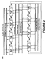
- Figure 2 illustrates a block diagram of an exemplary programmable digital device having a plurality of programmable digital circuit blocks in accordance with an embodiment of the present invention.
- Figure 3 illustrates a block diagram of a timer configuration of a programmable digital circuit block in accordance with an embodiment of the present invention.
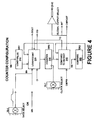
- Figure 4 illustrates a block diagram of a counter configuration of a programmable digital circuit block in accordance with an embodiment of the present invention.
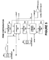
- FIG. 5 illustrates a block diagram of a pulse width modulator (PWM) configuration of a programmable digital circuit block in accordance with an embodiment of the present invention.
- PWM pulse width modulator
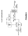
- Figure 6 illustrates a block diagram of a UART transmitter configuration of a programmable digital circuit block in accordance with an embodiment of the present invention.
- Figure 7 illustrates a block diagram of a UART receiver configuration of a programmable digital circuit block in accordance with an embodiment of the present invention.
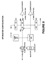
- Figure 8 illustrates a block diagram of a SPI Master configuration of a programmable digital circuit block in accordance with an embodiment of the present invention.
- Figure 9 illustrates a block diagram of a SPI Slave configuration of a programmable digital circuit block in accordance with an embodiment of the present invention.
- Figure 1 illustrates a programmable digital circuit block 100 in accordance with an embodiment of the present invention.
- the programmable digital circuit block 100 is the foundation of a new digital configurable macro architecture of the present invention.
- the digital configurable macro architecture is well suited for microcontroller or controller designs.
- the design of the programmable digital circuit block 100 in the digital configurable macro architecture was developed after examining and studying conventional microcontrollers to determine the types of digital functions that were implemented within various conventional microcontrollers. It was discovered that there were not very many different types of digital functions demanded in microcontroller applications. Furthermore, it was determined that these different types of digital functions had many circuit components in common. Moreover, it was determined that the digital functions were generally implemented as 8-bit or multiples of 8-bits because their length was generally based on the length of standard buses. This led to the development of the programmable digital circuit blocks 100, the building block of the digital configurable macro architecture.
- the programmable digital circuit block 100 is an 8-bit circuit module that can be programmed to perform any one of a variety of predetermined digital functions (which are useful in microcontroller applications) by changing the contents of a few configuration registers 50 therein, unlike a FPGA which is a generic device that can be programmed to perform any arbitrary digital function.
- the circuit components of the programmable digital circuit block 100 are designed for reuse in several of the predetermined digital functions such that to minimize the size of the programmable digital circuit block 100.
- the programmable digital circuit block 100 is highly efficient in terms of die area.
- the programmable digital circuit block 100 can be configured as a timer, a counter, a pulse width modulator (PWM), a cyclic redundancy generator/checker (CRC), a pseudo random sequence generator (PRS), a dead zone delay, a UART (universal asynchronous receiver-transmitter) transmitter, a UART (universal asynchronous receiver-transmitter) receiver, a SPI (serial peripheral interface) Master, or a SPI (serial peripheral interface) Slave.
- PWM pulse width modulator
- CRC cyclic redundancy generator/checker
- PRS pseudo random sequence generator
- the programmable digital circuit block 100 can be configured as a timer, a counter, a pulse width modulator (PWM), a cyclic redundancy generator/checker (CRC), a pseudo random sequence generator (PRS), or a dead zone delay, whereas the digital communication functions (e.g., UART and SPI) are eliminated to further reduce the size of the programmable digital circuit block 100.
- the user selects the digital function that is needed and configures the programmable digital circuit block 100 accordingly.
- the programmable digital circuit block 100 can be designed to implement other digital functions.
- a design can have an array of programmable digital circuit blocks 100 which can be configured to coupled together in series or in parallel to handle more complex digital functions or to increase precision.
- a 24-bit timer can be designed by coupling three 8-bit programmable digital circuit blocks 100 that have been individually configured as 8-bit timers.
- the 8-bit timer can be extended to 16- or 32-bit digital functions by coupling multiple programmable digital circuit blocks 100 together.
- a first programmable digital circuit block that is configured as a CRC generator can feed a second programmable digital circuit block that is configured as a serial output communication port, reducing device programming and increasing performance.
- the configuration of the programmable digital circuit block 100 is determined by its configuration registers 50.
- the programmable digital circuit block 100 generally has one or more configuration registers 50. This provides much flexibility.
- the configuration of the programmable digital circuit block 100 is fast and easy to configure and re-configure since changes in configuration are accomplished by changing the contents of the configuration registers 50, whereas the contents are generally a small number of configuration data bits.
- the programmable digital circuit block 100 is dynamically configurable from one predetermined digital function to another predetermined digital function for real-time processing.
- FPGAs need to have their look-up tables re-programmed in order to have them implement a new digital function, a time-consuming task that is not done in real-time processing.
- the programmable digital circuit block 100 includes one or more configuration registers 50, one or more data registers 40, a plurality of selectable logic circuits 30, one or more configurable inputs 20, one or more configurable outputs 10, one or more cascade outputs 60, one or more cascade inputs 70, a clock input 80, and a system input 90. It should be understood that the programmable digital circuit block 100 can have other designs including lengths other than 8-bits.
- the configuration registers 50 are programmed via the system bus 90. Any device, such as a microprocessor using data stored in a RAM or flash memory, can program (or write to) the configuration registers.
- the configuration registers 50 receive and store a plurality of configuration data corresponding to any one of the plurality of predetermined digital function described above.
- the programmed configuration registers 50 configure the programmable digital circuit block 100 to perform any one of the predetermined digital functions based on the configuration data.
- the configuration registers 50 can be dynamically programmed with the configuration data for real-time processing.
- the configuration data includes (1) bits for indicating one of the predetermined digital functions and configuring the selectable logic circuits 30, (2) bits for configuring and selecting the configurable inputs 20 and the configurable outputs 10 and the clock input 80, (3) bits for indicating the mode of the predetermined digital function (e.g., parity, no parity, etc.), (4) bits for indicating the length of the predetermine digital function if several programmable digital circuit block 100 are coupled together (e.g., 8-bit, 16-bit, 24-bit, etc.), and (5) bits for indicating and configuring the interface between adjacent programmable digital circuit blocks 100 that are coupled together (e.g., configuring and selecting the cascade inputs 70 and the cascade outputs 60 for serial or parallel interfacing).
- the mode of the predetermined digital function e.g., parity, no parity, etc.
- bits for indicating the length of the predetermine digital function if several programmable digital circuit block 100 are coupled together e.g., 8-bit, 16-bit, 24-bit,
- the number of bits in the configuration data is sufficiently small to enable the configuration registers 50 to be programmed on-the-fly so that the programmable digital circuit block 100 can be dynamically configured and interfaced.
- the programmable digital circuit blocks 100 can be configured as a timer for a first length of time, re-configured as a counter for a second length of time, re-configured as a PWM for a third length of time, and so on, for real-time processing.
- connections 50A-50F between the configuration registers 50 and other components of the programmable digital circuit block 100 enable the configuration registers 50 to properly configure the programmable digital circuit block 100 to any one of the predetermined digital functions and to properly interface the programmable digital circuit block 100 with other programmable digital circuit blocks in series or in parallel.
- the selectable logic circuits 30 are tailored such that they have a minimum set of circuit resources that can be programmed by the configuration registers 50 to implement any one of a variety of predetermined digital functions, unlike the FPGA where a substantial amount of circuit resources may remain unused.
- the design and structure of the selectable logic circuits 30 are dependent on the predetermined digital functions such that to minimize the size of the programmable digital circuit block 100.
- the fixed number of digital functions for the programmable digital circuit block 100 substantially influences the design of the programmable digital circuit block 100, providing cost savings and improving performance.
- the configuration registers 50 configure and select any of the selectable logic circuits 30 to perform one of the predetermined digital functions based on the configuration data. More importantly, the selectable logic circuits 30 are reused in several of the predetermined digital functions as will be illustrated below, ensuring the size efficiency of the programmable digital circuit block 100.
- the selectable logic circuits 30 include a plurality of logic gates.
- the selectable logic circuits 30 realize any one of the variety of predetermined digital functions by using the data registers 40 to receive data, load data, capture data, etc.
- the data registers 40 are also reused in several of the predetermined digital functions as will be illustrated below.
- the cascade outputs 60 and the cascade inputs 70 are selected and configured according to the configuration data.
- the cascade outputs 60 allow the programmable digital circuit block 100 to output signals for directly interfacing with adjacent or neighboring programmable digital circuit blocks.
- the cascade inputs 70 allow the adjacent or neighboring programmable digital circuit blocks to send signals that directly interface and are received by the programmable digital circuit block 100.
- the cascade outputs 60 and the cascade inputs 70 enable multiple programmable digital circuit blocks to seamlessly interface to handle more complex digital functions or to increase precision as described above (e.g., 32-bit timer, CRC generator and SPI Master, 24-bit counter, etc.).
- FIG. 2 illustrates a block diagram of an exemplary programmable digital device 200 having a plurality of programmable digital circuit blocks 210A-210H in accordance with an embodiment of the present invention.
- the plurality of programmable digital circuit blocks 210A-210H includes a first group and a second group.
- the first group includes the programmable digital circuit blocks 210A-210B and 210E-210F.
- each programmable digital circuit block of the first group can be configured as a timer, a counter, a pulse width modulator (PWM), a cyclic redundancy generator/checker (CRC), a pseudo random sequence generator (PRS), or a dead zone delay.
- PWM pulse width modulator
- CRC cyclic redundancy generator/checker
- PRS pseudo random sequence generator
- the second group includes the programmable digital circuit blocks 210C-210D and 210G-210H.
- each programmable digital circuit block of the second group can be configured as a timer, a counter, a pulse width modulator (PWM), a cyclic redundancy generator/checker (CRC), a pseudo random sequence generator (PRS), a dead zone delay, a UART (universal asynchronous receiver-transmitter) transmitter, a UART (universal asynchronous receiver-transmitter) receiver, a SPI (serial peripheral interface) Master, or a SPI (serial peripheral interface) Slave.
- PWM pulse width modulator
- CRC cyclic redundancy generator/checker
- PRS pseudo random sequence generator
- cascade lines 205 enable the programmable digital circuit blocks 210A-210H to seamlessly interface to handle more complex digital functions or to increase precision.
- a 32-bit counter can be designed by coupling four 8-bit programmable digital circuit blocks that have been individually configured as 8-bit counters.
- the 8-bit counter can be extended to 16- or 24-bit digital functions by coupling multiple programmable digital circuit blocks together.
- a first programmable digital circuit block that is configured as a CRC generator can feed a second programmable digital circuit block that is configured as a serial output communication port, reducing device programming and increasing performance.
- the exemplary programmable digital device 200 includes a signal bus for digitized analog signals, a clock bus, a system bus for programming the programmable digital circuit blocks 210A-210H, and a plurality of global data buses for transmitting data to/from the programmable digital circuit blocks 210A-210H.
- Figure 3 illustrates a block diagram of a timer configuration of a programmable digital circuit block in accordance with an embodiment of the present invention.
- Figure 4 illustrates a block diagram of a counter configuration of a programmable digital circuit block in accordance with an embodiment of the present invention.
- Figure 5 illustrates a block diagram of a pulse width modulator (PWM) configuration of a programmable digital circuit block in accordance with an embodiment of the present invention.
- PWM pulse width modulator
- the selectable logic circuits 320 and 340 are reused for the timer, counter, and PWM configurations. Moreover, the first data register 310, the second data register 330, and the third data register 350 of the programmable digital circuit block are reused for the timer, counter, and PWM configurations.
- the configuration data loaded onto the configuration registers determines how the data registers 310, 330, and 350 are to be used, what operation is to be performed on the data by the selectable logic circuits 320 and 340, where the input data is selected from (e.g., system bus (SB), signal bus, global bus, etc.), where the output data is transmitted, what clock signal is to be used, what are the cascade inputs (e.g., DIN, Cl, etc.) from other programmable digital circuit blocks, what are the cascade outputs (e.g., DOUT, CO, etc.) to other programmable digital circuit blocks, when to generate an interrupt (INT), and what is the data flow within the programmable digital circuit block so that the programmable digital circuit block can properly perform any one of the predetermined digital functions.
- SB system bus
- INT interrupt
- Figure 6 illustrates a block diagram of a UART transmitter configuration of a programmable digital circuit block in accordance with an embodiment of the present invention.
- Figure 7 illustrates a block diagram of a UART receiver configuration of a programmable digital circuit block in accordance with an embodiment of the present invention.
- Figure 8 illustrates a block diagram of a SPI Master configuration of a programmable digital circuit block in accordance with an embodiment of the present invention.
- Figure 9 illustrates a block diagram of a SPI Slave configuration of a programmable digital circuit block in accordance with an embodiment of the present invention.
- the selectable logic circuits 410 and 420 are reused for the UART transmitter, the UART receiver, the SPI Master, and the SPI Slave configurations. Moreover, the first data register 310, the second data register 330, and the third data register 350 of the programmable digital circuit block are reused in several of the UART transmitter, the UART receiver, the SPI Master, and the SPI Slave configurations. However, the selectable logic circuit 430 is used in the UART transmitter configuration of Figure 6 since the UART protocol requires that particular protocol bits (e.g., start bits, stop bits, etc.) to be generated by the UART transmitter.
- particular protocol bits e.g., start bits, stop bits, etc.
- Figures 3-9 illustrate that the programmable digital circuit block can be configured fast and easily. Furthermore, Figures 3-9 illustrate that the programmable digital circuit block is highly efficient in terms of die area.
Landscapes
- Engineering & Computer Science (AREA)
- Theoretical Computer Science (AREA)
- Physics & Mathematics (AREA)
- General Engineering & Computer Science (AREA)
- General Physics & Mathematics (AREA)
- Computer Hardware Design (AREA)
- Chemical & Material Sciences (AREA)
- Crystallography & Structural Chemistry (AREA)
- Logic Circuits (AREA)
- Stored Programmes (AREA)
Applications Claiming Priority (6)
| Application Number | Priority Date | Filing Date | Title |
|---|---|---|---|
| US24370800P | 2000-10-26 | 2000-10-26 | |
| US243708P | 2000-10-26 | ||
| US909109 | 2001-07-18 | ||
| US09/909,045 US6507214B1 (en) | 2000-10-26 | 2001-07-18 | Digital configurable macro architecture |
| US909045 | 2001-07-18 | ||
| US09/909,109 US6603330B1 (en) | 2000-10-26 | 2001-07-18 | Configuring digital functions in a digital configurable macro architecture |
Publications (2)
| Publication Number | Publication Date |
|---|---|
| EP1220107A2 true EP1220107A2 (fr) | 2002-07-03 |
| EP1220107A3 EP1220107A3 (fr) | 2005-01-05 |
Family
ID=27399681
Family Applications (1)
| Application Number | Title | Priority Date | Filing Date |
|---|---|---|---|
| EP01125550A Ceased EP1220107A3 (fr) | 2000-10-26 | 2001-10-25 | Dispositif numérique programmable |
Country Status (2)
| Country | Link |
|---|---|
| EP (1) | EP1220107A3 (fr) |
| TW (1) | TW533359B (fr) |
Cited By (3)
| Publication number | Priority date | Publication date | Assignee | Title |
|---|---|---|---|---|
| US7680967B2 (en) * | 2005-01-27 | 2010-03-16 | Innovasic, Inc. | Configurable application specific standard product with configurable I/O |
| CN106996938A (zh) * | 2017-03-07 | 2017-08-01 | 天津大学 | 超宽带微波目标检测的fpga成像系统 |
| CN111240244A (zh) * | 2020-01-16 | 2020-06-05 | 中科亿海微电子科技(苏州)有限公司 | 一种适用于fpga的可编程脉冲产生装置、电路及方法 |
Citations (2)
| Publication number | Priority date | Publication date | Assignee | Title |
|---|---|---|---|---|
| EP0668659A2 (fr) * | 1994-02-17 | 1995-08-23 | Pilkington Germany (no. 2) Limited | Circuit intégré d'application spécifique (ASIC) réconfigurable |
| US5835405A (en) * | 1993-12-13 | 1998-11-10 | Lattice Semiconductor Corporation | Application specific modules in a programmable logic device |
Family Cites Families (4)
| Publication number | Priority date | Publication date | Assignee | Title |
|---|---|---|---|---|
| US4694416A (en) * | 1985-02-25 | 1987-09-15 | General Electric Company | VLSI programmable digital signal processor |
| US5887165A (en) * | 1996-06-21 | 1999-03-23 | Mirage Technologies, Inc. | Dynamically reconfigurable hardware system for real-time control of processes |
| DE19651075A1 (de) * | 1996-12-09 | 1998-06-10 | Pact Inf Tech Gmbh | Einheit zur Verarbeitung von numerischen und logischen Operationen, zum Einsatz in Prozessoren (CPU's), Mehrrechnersystemen, Datenflußprozessoren (DFP's), digitalen Signal Prozessoren (DSP's) oder dergleichen |
| US6094726A (en) * | 1998-02-05 | 2000-07-25 | George S. Sheng | Digital signal processor using a reconfigurable array of macrocells |
-
2001
- 2001-10-25 EP EP01125550A patent/EP1220107A3/fr not_active Ceased
- 2001-10-26 TW TW90126526A patent/TW533359B/zh not_active IP Right Cessation
Patent Citations (2)
| Publication number | Priority date | Publication date | Assignee | Title |
|---|---|---|---|---|
| US5835405A (en) * | 1993-12-13 | 1998-11-10 | Lattice Semiconductor Corporation | Application specific modules in a programmable logic device |
| EP0668659A2 (fr) * | 1994-02-17 | 1995-08-23 | Pilkington Germany (no. 2) Limited | Circuit intégré d'application spécifique (ASIC) réconfigurable |
Cited By (3)
| Publication number | Priority date | Publication date | Assignee | Title |
|---|---|---|---|---|
| US7680967B2 (en) * | 2005-01-27 | 2010-03-16 | Innovasic, Inc. | Configurable application specific standard product with configurable I/O |
| CN106996938A (zh) * | 2017-03-07 | 2017-08-01 | 天津大学 | 超宽带微波目标检测的fpga成像系统 |
| CN111240244A (zh) * | 2020-01-16 | 2020-06-05 | 中科亿海微电子科技(苏州)有限公司 | 一种适用于fpga的可编程脉冲产生装置、电路及方法 |
Also Published As
| Publication number | Publication date |
|---|---|
| TW533359B (en) | 2003-05-21 |
| EP1220107A3 (fr) | 2005-01-05 |
Similar Documents
| Publication | Publication Date | Title |
|---|---|---|
| US6603330B1 (en) | Configuring digital functions in a digital configurable macro architecture | |
| US6507214B1 (en) | Digital configurable macro architecture | |
| US6825689B1 (en) | Configurable input/output interface for a microcontroller | |
| CN104050146B (zh) | 一种微控制单元mcu芯片 | |
| EP2722989B1 (fr) | Procédés et appareil permettant de construire des réseaux d'interconnexion de bus à l'aide des ressources d'interconnexion programmables | |
| EP2031518A2 (fr) | Circuit | |
| CN104424154A (zh) | 通用串行外围接口 | |
| CN102262604B (zh) | 一种并发访问方法、系统及接口装置 | |
| Bomar | Implementation of microprogrammed control in FPGAs | |
| US7624209B1 (en) | Method of and circuit for enabling variable latency data transfers | |
| TW201705006A (zh) | 積體電路之輸入及輸出(二) | |
| US20020133654A1 (en) | Method and apparatus for bus arbitration capable of effectively altering a priority order | |
| US10049071B2 (en) | Programmable logic unit | |
| EP1220107A2 (fr) | Dispositif numérique programmable | |
| US8706931B1 (en) | Tool selection and implementation of port adapters | |
| CN111103959B (zh) | 寄存器复位系统及芯片 | |
| EP1213653A2 (fr) | Interface de machine d'état programmable | |
| US6621295B1 (en) | Reconfigurable priority encoding | |
| CN114168506B (zh) | 多通道dma控制传输装置 | |
| US9438525B2 (en) | Scheduling module and method thereof | |
| CN107577438B (zh) | 现场可编程门阵列中闪存的存储空间的划分方法及装置 | |
| US6253263B1 (en) | System with logic gates having a progressive number of inputs connected to a first connection matrix receiving signals to be arbitrated from peripheral devices | |
| CN216118784U (zh) | 双向引脚多功能复用电路、fpga器件及多功能复用系统 | |
| US7346860B1 (en) | User non-volatile memory interface megafunction | |
| CN100550654C (zh) | 输入/输出电路串行转并行的装置及方法 |
Legal Events
| Date | Code | Title | Description |
|---|---|---|---|
| PUAI | Public reference made under article 153(3) epc to a published international application that has entered the european phase |
Free format text: ORIGINAL CODE: 0009012 |
|
| AK | Designated contracting states |
Kind code of ref document: A2 Designated state(s): AT BE CH CY DE DK ES FI FR GB GR IE IT LI LU MC NL PT SE TR |
|
| AX | Request for extension of the european patent |
Free format text: AL;LT;LV;MK;RO;SI |
|
| PUAL | Search report despatched |
Free format text: ORIGINAL CODE: 0009013 |
|
| AK | Designated contracting states |
Kind code of ref document: A3 Designated state(s): AT BE CH CY DE DK ES FI FR GB GR IE IT LI LU MC NL PT SE TR |
|
| AX | Request for extension of the european patent |
Extension state: AL LT LV MK RO SI |
|
| 17P | Request for examination filed |
Effective date: 20050627 |
|
| AKX | Designation fees paid |
Designated state(s): AT BE CH CY DE DK ES FI FR GB GR IE IT LI LU MC NL PT SE TR |
|
| AXX | Extension fees paid |
Extension state: SI Payment date: 20050627 Extension state: RO Payment date: 20050627 Extension state: MK Payment date: 20050627 Extension state: LV Payment date: 20050627 Extension state: LT Payment date: 20050627 Extension state: AL Payment date: 20050627 |
|
| 17Q | First examination report despatched |
Effective date: 20071002 |
|
| RAP1 | Party data changed (applicant data changed or rights of an application transferred) |
Owner name: CYPRESS SEMICONDUCTOR CORPORATION |
|
| STAA | Information on the status of an ep patent application or granted ep patent |
Free format text: STATUS: EXAMINATION IS IN PROGRESS |
|
| STAA | Information on the status of an ep patent application or granted ep patent |
Free format text: STATUS: THE APPLICATION HAS BEEN REFUSED |
|
| 18R | Application refused |
Effective date: 20200201 |