EP1213767A2 - Nitride compound semiconductor element - Google Patents
Nitride compound semiconductor element Download PDFInfo
- Publication number
- EP1213767A2 EP1213767A2 EP01128995A EP01128995A EP1213767A2 EP 1213767 A2 EP1213767 A2 EP 1213767A2 EP 01128995 A EP01128995 A EP 01128995A EP 01128995 A EP01128995 A EP 01128995A EP 1213767 A2 EP1213767 A2 EP 1213767A2
- Authority
- EP
- European Patent Office
- Prior art keywords
- underlayer
- semiconductor element
- semiconductor
- conductive layer
- substrate
- Prior art date
- Legal status (The legal status is an assumption and is not a legal conclusion. Google has not performed a legal analysis and makes no representation as to the accuracy of the status listed.)
- Withdrawn
Links
- 239000004065 semiconductor Substances 0.000 title claims abstract description 148
- -1 Nitride compound Chemical class 0.000 title claims description 4
- 239000000758 substrate Substances 0.000 claims abstract description 74
- 239000013078 crystal Substances 0.000 claims description 49
- 150000004767 nitrides Chemical class 0.000 claims description 49
- 229910052782 aluminium Inorganic materials 0.000 claims description 22
- 229910052733 gallium Inorganic materials 0.000 claims description 22
- 229910052738 indium Inorganic materials 0.000 claims description 22
- 238000000034 method Methods 0.000 claims description 21
- 229910052594 sapphire Inorganic materials 0.000 claims description 21
- 239000010980 sapphire Substances 0.000 claims description 21
- 239000000463 material Substances 0.000 claims description 9
- 238000002488 metal-organic chemical vapour deposition Methods 0.000 claims description 6
- 230000005669 field effect Effects 0.000 claims description 2
- 238000005121 nitriding Methods 0.000 description 14
- QGZKDVFQNNGYKY-UHFFFAOYSA-N Ammonia Chemical compound N QGZKDVFQNNGYKY-UHFFFAOYSA-N 0.000 description 11
- VYPSYNLAJGMNEJ-UHFFFAOYSA-N Silicium dioxide Chemical compound O=[Si]=O VYPSYNLAJGMNEJ-UHFFFAOYSA-N 0.000 description 10
- 229910002704 AlGaN Inorganic materials 0.000 description 9
- IJGRMHOSHXDMSA-UHFFFAOYSA-N Atomic nitrogen Chemical compound N#N IJGRMHOSHXDMSA-UHFFFAOYSA-N 0.000 description 6
- 229910000069 nitrogen hydride Inorganic materials 0.000 description 6
- 229910001218 Gallium arsenide Inorganic materials 0.000 description 5
- 230000015572 biosynthetic process Effects 0.000 description 5
- 229910052681 coesite Inorganic materials 0.000 description 5
- 229910052906 cristobalite Inorganic materials 0.000 description 5
- 239000000377 silicon dioxide Substances 0.000 description 5
- 229910052682 stishovite Inorganic materials 0.000 description 5
- 229910052905 tridymite Inorganic materials 0.000 description 5
- JLTRXTDYQLMHGR-UHFFFAOYSA-N trimethylaluminium Chemical compound C[Al](C)C JLTRXTDYQLMHGR-UHFFFAOYSA-N 0.000 description 5
- 239000007789 gas Substances 0.000 description 4
- 238000004519 manufacturing process Methods 0.000 description 4
- 230000000644 propagated effect Effects 0.000 description 4
- 238000009792 diffusion process Methods 0.000 description 3
- 229910052757 nitrogen Inorganic materials 0.000 description 3
- BLRPTPMANUNPDV-UHFFFAOYSA-N Silane Chemical compound [SiH4] BLRPTPMANUNPDV-UHFFFAOYSA-N 0.000 description 2
- 238000004833 X-ray photoelectron spectroscopy Methods 0.000 description 2
- 229910021529 ammonia Inorganic materials 0.000 description 2
- 238000004458 analytical method Methods 0.000 description 2
- 239000000470 constituent Substances 0.000 description 2
- 230000003247 decreasing effect Effects 0.000 description 2
- 239000002994 raw material Substances 0.000 description 2
- 230000003746 surface roughness Effects 0.000 description 2
- KLSJWNVTNUYHDU-UHFFFAOYSA-N Amitrole Chemical compound NC1=NC=NN1 KLSJWNVTNUYHDU-UHFFFAOYSA-N 0.000 description 1
- JMASRVWKEDWRBT-UHFFFAOYSA-N Gallium nitride Chemical compound [Ga]#N JMASRVWKEDWRBT-UHFFFAOYSA-N 0.000 description 1
- 229910010092 LiAlO2 Inorganic materials 0.000 description 1
- 229910010936 LiGaO2 Inorganic materials 0.000 description 1
- 229910026161 MgAl2O4 Inorganic materials 0.000 description 1
- QAOWNCQODCNURD-UHFFFAOYSA-N Sulfuric acid Chemical compound OS(O)(=O)=O QAOWNCQODCNURD-UHFFFAOYSA-N 0.000 description 1
- 229910007948 ZrB2 Inorganic materials 0.000 description 1
- 239000000654 additive Substances 0.000 description 1
- 230000000996 additive effect Effects 0.000 description 1
- 230000004888 barrier function Effects 0.000 description 1
- VWZIXVXBCBBRGP-UHFFFAOYSA-N boron;zirconium Chemical compound B#[Zr]#B VWZIXVXBCBBRGP-UHFFFAOYSA-N 0.000 description 1
- 239000000969 carrier Substances 0.000 description 1
- 239000012159 carrier gas Substances 0.000 description 1
- 230000015556 catabolic process Effects 0.000 description 1
- 230000001413 cellular effect Effects 0.000 description 1
- 238000004891 communication Methods 0.000 description 1
- 238000007796 conventional method Methods 0.000 description 1
- 230000001419 dependent effect Effects 0.000 description 1
- 238000011161 development Methods 0.000 description 1
- 239000012535 impurity Substances 0.000 description 1
- 230000005764 inhibitory process Effects 0.000 description 1
- 230000007774 longterm Effects 0.000 description 1
- 238000010295 mobile communication Methods 0.000 description 1
- 238000012986 modification Methods 0.000 description 1
- 230000004048 modification Effects 0.000 description 1
- 230000003287 optical effect Effects 0.000 description 1
- 238000012545 processing Methods 0.000 description 1
- 238000012827 research and development Methods 0.000 description 1
- 229920006395 saturated elastomer Polymers 0.000 description 1
- 125000006850 spacer group Chemical group 0.000 description 1
- 229910052596 spinel Inorganic materials 0.000 description 1
- 229910052725 zinc Inorganic materials 0.000 description 1
Images
Classifications
-
- H—ELECTRICITY
- H01—ELECTRIC ELEMENTS
- H01L—SEMICONDUCTOR DEVICES NOT COVERED BY CLASS H10
- H01L29/00—Semiconductor devices specially adapted for rectifying, amplifying, oscillating or switching and having potential barriers; Capacitors or resistors having potential barriers, e.g. a PN-junction depletion layer or carrier concentration layer; Details of semiconductor bodies or of electrodes thereof ; Multistep manufacturing processes therefor
- H01L29/66—Types of semiconductor device ; Multistep manufacturing processes therefor
- H01L29/66007—Multistep manufacturing processes
- H01L29/66075—Multistep manufacturing processes of devices having semiconductor bodies comprising group 14 or group 13/15 materials
- H01L29/66227—Multistep manufacturing processes of devices having semiconductor bodies comprising group 14 or group 13/15 materials the devices being controllable only by the electric current supplied or the electric potential applied, to an electrode which does not carry the current to be rectified, amplified or switched, e.g. three-terminal devices
- H01L29/66234—Bipolar junction transistors [BJT]
- H01L29/6631—Bipolar junction transistors [BJT] with an active layer made of a group 13/15 material
- H01L29/66318—Heterojunction transistors
-
- H—ELECTRICITY
- H01—ELECTRIC ELEMENTS
- H01L—SEMICONDUCTOR DEVICES NOT COVERED BY CLASS H10
- H01L21/00—Processes or apparatus adapted for the manufacture or treatment of semiconductor or solid state devices or of parts thereof
- H01L21/02—Manufacture or treatment of semiconductor devices or of parts thereof
- H01L21/02104—Forming layers
- H01L21/02365—Forming inorganic semiconducting materials on a substrate
- H01L21/02367—Substrates
- H01L21/0237—Materials
- H01L21/0242—Crystalline insulating materials
-
- H—ELECTRICITY
- H01—ELECTRIC ELEMENTS
- H01L—SEMICONDUCTOR DEVICES NOT COVERED BY CLASS H10
- H01L21/00—Processes or apparatus adapted for the manufacture or treatment of semiconductor or solid state devices or of parts thereof
- H01L21/02—Manufacture or treatment of semiconductor devices or of parts thereof
- H01L21/02104—Forming layers
- H01L21/02365—Forming inorganic semiconducting materials on a substrate
- H01L21/02436—Intermediate layers between substrates and deposited layers
- H01L21/02439—Materials
- H01L21/02455—Group 13/15 materials
- H01L21/02458—Nitrides
-
- H—ELECTRICITY
- H01—ELECTRIC ELEMENTS
- H01L—SEMICONDUCTOR DEVICES NOT COVERED BY CLASS H10
- H01L21/00—Processes or apparatus adapted for the manufacture or treatment of semiconductor or solid state devices or of parts thereof
- H01L21/02—Manufacture or treatment of semiconductor devices or of parts thereof
- H01L21/02104—Forming layers
- H01L21/02365—Forming inorganic semiconducting materials on a substrate
- H01L21/02518—Deposited layers
- H01L21/02521—Materials
- H01L21/02538—Group 13/15 materials
- H01L21/0254—Nitrides
-
- H—ELECTRICITY
- H01—ELECTRIC ELEMENTS
- H01L—SEMICONDUCTOR DEVICES NOT COVERED BY CLASS H10
- H01L21/00—Processes or apparatus adapted for the manufacture or treatment of semiconductor or solid state devices or of parts thereof
- H01L21/02—Manufacture or treatment of semiconductor devices or of parts thereof
- H01L21/02104—Forming layers
- H01L21/02365—Forming inorganic semiconducting materials on a substrate
- H01L21/02612—Formation types
- H01L21/02617—Deposition types
- H01L21/0262—Reduction or decomposition of gaseous compounds, e.g. CVD
-
- H—ELECTRICITY
- H01—ELECTRIC ELEMENTS
- H01L—SEMICONDUCTOR DEVICES NOT COVERED BY CLASS H10
- H01L29/00—Semiconductor devices specially adapted for rectifying, amplifying, oscillating or switching and having potential barriers; Capacitors or resistors having potential barriers, e.g. a PN-junction depletion layer or carrier concentration layer; Details of semiconductor bodies or of electrodes thereof ; Multistep manufacturing processes therefor
- H01L29/66—Types of semiconductor device ; Multistep manufacturing processes therefor
- H01L29/66007—Multistep manufacturing processes
- H01L29/66075—Multistep manufacturing processes of devices having semiconductor bodies comprising group 14 or group 13/15 materials
- H01L29/66227—Multistep manufacturing processes of devices having semiconductor bodies comprising group 14 or group 13/15 materials the devices being controllable only by the electric current supplied or the electric potential applied, to an electrode which does not carry the current to be rectified, amplified or switched, e.g. three-terminal devices
- H01L29/66409—Unipolar field-effect transistors
- H01L29/66446—Unipolar field-effect transistors with an active layer made of a group 13/15 material, e.g. group 13/15 velocity modulation transistor [VMT], group 13/15 negative resistance FET [NERFET]
- H01L29/66462—Unipolar field-effect transistors with an active layer made of a group 13/15 material, e.g. group 13/15 velocity modulation transistor [VMT], group 13/15 negative resistance FET [NERFET] with a heterojunction interface channel or gate, e.g. HFET, HIGFET, SISFET, HJFET, HEMT
-
- H—ELECTRICITY
- H01—ELECTRIC ELEMENTS
- H01L—SEMICONDUCTOR DEVICES NOT COVERED BY CLASS H10
- H01L29/00—Semiconductor devices specially adapted for rectifying, amplifying, oscillating or switching and having potential barriers; Capacitors or resistors having potential barriers, e.g. a PN-junction depletion layer or carrier concentration layer; Details of semiconductor bodies or of electrodes thereof ; Multistep manufacturing processes therefor
- H01L29/66—Types of semiconductor device ; Multistep manufacturing processes therefor
- H01L29/66007—Multistep manufacturing processes
- H01L29/66075—Multistep manufacturing processes of devices having semiconductor bodies comprising group 14 or group 13/15 materials
- H01L29/66227—Multistep manufacturing processes of devices having semiconductor bodies comprising group 14 or group 13/15 materials the devices being controllable only by the electric current supplied or the electric potential applied, to an electrode which does not carry the current to be rectified, amplified or switched, e.g. three-terminal devices
- H01L29/66409—Unipolar field-effect transistors
- H01L29/66848—Unipolar field-effect transistors with a Schottky gate, i.e. MESFET
- H01L29/66856—Unipolar field-effect transistors with a Schottky gate, i.e. MESFET with an active layer made of a group 13/15 material
-
- H—ELECTRICITY
- H01—ELECTRIC ELEMENTS
- H01L—SEMICONDUCTOR DEVICES NOT COVERED BY CLASS H10
- H01L29/00—Semiconductor devices specially adapted for rectifying, amplifying, oscillating or switching and having potential barriers; Capacitors or resistors having potential barriers, e.g. a PN-junction depletion layer or carrier concentration layer; Details of semiconductor bodies or of electrodes thereof ; Multistep manufacturing processes therefor
- H01L29/02—Semiconductor bodies ; Multistep manufacturing processes therefor
- H01L29/12—Semiconductor bodies ; Multistep manufacturing processes therefor characterised by the materials of which they are formed
- H01L29/20—Semiconductor bodies ; Multistep manufacturing processes therefor characterised by the materials of which they are formed including, apart from doping materials or other impurities, only AIIIBV compounds
- H01L29/2003—Nitride compounds
Definitions
- the underlayer thicker, some tensile stresses may be exerted on the underlayer and thus, some cracks may be created in the underlayer.
- the material composition is varied continuously or stepwisely from the substrate toward the conductive layer.
- a TMG, a NH 3 and a SiH 4 were flown at an average rate of 1m/sec, to epitaxially grow a Si-doped n-GaN film as a conductive layer.
- the dislocation density of the n-GaN film was 2 ⁇ 10 8 /cm 2
- the FWHM in X-ray rocking curve of the n-GaN film was 120 seconds at (002) reflection.
- the carrier density of the n-GaN film was 8 ⁇ 10 16 /cm 3
- the mobility at room temperature was 800cm 2 /V ⁇ sec.
- the HBT 30 shown in Fig. 3 although the HBT 30 has an npn-type junction structure, it may have a pnp-type junction structure by changing the conduction types of the semiconductor layers of the HBT 30. Moreover, for developing the crystal qualities of the conductive layers 13-16 formed on the underlayer 2, a buffer layer or a multilayered structure such as a distorted superlattice structure may be provided between the underlayer 2 and the conductive layer 13.
Landscapes
- Engineering & Computer Science (AREA)
- Microelectronics & Electronic Packaging (AREA)
- Power Engineering (AREA)
- Condensed Matter Physics & Semiconductors (AREA)
- General Physics & Mathematics (AREA)
- Manufacturing & Machinery (AREA)
- Computer Hardware Design (AREA)
- Physics & Mathematics (AREA)
- Chemical & Material Sciences (AREA)
- Ceramic Engineering (AREA)
- Materials Engineering (AREA)
- Crystallography & Structural Chemistry (AREA)
- Junction Field-Effect Transistors (AREA)
- Bipolar Transistors (AREA)
- Chemical Vapour Deposition (AREA)
- Crystals, And After-Treatments Of Crystals (AREA)
Abstract
Description
- This invention relates to a semiconductor element, particularly usable for a field-effect transistor (FET), a high electron mobility transistor (HEMT), a heterojunction bipolar transistor (HBT) or the like.
- With the recent development of cellular phone technique and optical communication technique, low electric power consumable and high output electron devices having high frequency properties are remarkably desired.
As such an electron device, conventionally, a Si device and a GaAs device have been employed. However, since these device does not have sufficiently high frequency properties, a new high output electron device is keenly desired. - In this point of view, a HEMT and a psudemorphic HEMT which are made of GaAs-based semiconductors are developed and practically used. Moreover, a high performance electron device such as a HEMT and a HBT made of InP-based semiconductor are researched and developed.
- However, such a high performance electron device is composed of plural semiconductor layers epitaxially grown on a given substrate, and has a much complicated structure. Moreover, micro processing technique is required in fabricating the electron device, so that the manufacturing cost of the electron device rises. In addition, the InP-based semiconductor is very expensive, so that alternatives are desired.
- In this point of view, recently, much attention is paid to a new electron device made of GaN-based semiconductor. Since the bandgap of the GaN semiconductor is 3.39eV, the GaN semiconductor can have a dielectric breakdown voltage tenfold as large as that of GaAs semiconductor and Si semiconductor. Moreover, the GaN semiconductor can have a large electron saturated drift velocity, it can have a larger performance index as an electron device than the GaAs semiconductor and the Si semiconductor. Therefore, the GaN semiconductor is prospected as a fundamental semiconductor for a high temperature device, a high output device and a high frequency device in engine controlling technique, electric power converting technique and mobile communication technique.
- Particularly, since an electron device of HEMT structure made of AlGaN or GaN semiconductor is developed by Khan et al. and published in "J. Appl. Phys. Lett.", 63(1993), pp1214-, such an electron device using GaN-based semiconductor has been intensely researched and developed all over the world. Such an electron device is generally formed by epitaxially growing given semiconductor layers on a sapphire substrate.
- However, since the lattice mismatch between the GaN-based semiconductor layer and the sapphire substrate is large, much misfit dislocations are created at the boundary between the semiconductor layer and substrate, and then, propagated in the semiconductor layer. As a result, much dislocations of 1010/cm2 order are created in the semiconductor layer, and thus, the electric properties of the electron device including the semiconductor layer are deteriorated. Therefore, under the present conditions, the performance of the electron device made of GaN-based semiconductor can not be sufficiently improved.
- In order to improve the crystal quality of the GaN-based semiconductor layer, such an attempt is made as to form a buffer layer between the semiconductor layer and the sapphire substrate or to employ a SiC substrate, a GaN substrate and another oxide substrate instead of the sapphire substrate, but the crystal quality of the GaN-based semiconductor layer formed on the substrate can not sufficiently improved.
- Moreover, such an ELO technique as forming a strip mask made of SiO2, etc. on a substrate has been developed. In this case, misfit dislocations created at the boundary between the GaN-based semiconductor layer and the substrate are propagated laterally in the region above the strip mask, and thus, the dislocation density of the semiconductor layer is decreased in between the adjacent strip portions of the mask.
- However, since the ELO technique requires a complicated process, the manufacturing cost of the electron device rises. Moreover, since the GaN semiconductor layer must be formed thicker so as to cover the strip mask, the substrate may be warped. If the ELO technique is employed in the practical process for manufacturing electron devices including the GaN-based semiconductor layers, most of the substrates to be employed and constituting the electron devices are warped and thus, broken. Therefore, the ELO technique can not be employed in the practical manufacturing process for the electron device.
- It is an object of the present invention to decrease the dislocation density of a semiconductor layer made of a nitride including at least one element selected from the group consisting of Al, Ga, and In and epitaxially grown, and thus, to provide a semiconductor element including such a semiconductor layer usable as a practical device such as a FET and a HEMT.
- In order to achieve the above object, this invention relates to a semiconductor element(a first semiconductor element), substantially including a substrate, an underlayer, epitaxially grown on the substrate, made of a first semiconductor nitride including at least Al element, the dislocation density of the underlayer being set to 1011/cm2 or below, the crystallinity of the underlayer being set to 90 seconds or below in full width at half maximum of X-ray rocking curve at (002) reflection, and a conductive layer, epitaxially grown on the underlayer, made of a second semiconductor nitride including at least one element selected from the group consisting of Al, Ga and In, the dislocation of the conductive layer being set to 1010/cm2 or below, the crystallinity of the conductive layer being set to 150 seconds or below in full width at half maximum of X-ray rocking curve at (002) reflection.
- This invention also relates to a semiconductor element(a second semiconductor element), substantially including a substrate,
an underlayer, epitaxially grown on the substrate, made of a first semiconductor nitride including at least one element selected from the group consisting of Al, Ga and In, the dislocation density of the underlayer being set to 1011/cm2 or below, the crystallinity of the underlayer being set to 90 seconds or below in full width at half maximum of X-ray rocking curve at (002) reflection, a carrier moving layer, epitaxially grown on the underlayer, made of a second semiconductor nitride including at least one element selected from the group consisting of Al, Ga and In, the dislocation of the carrier moving layer being set to 1010/cm2 or below, the crystallinity of the carrier moving layer being set to 150 seconds or below in full width at half maximum of X-ray rocking curve at (002) reflection, and
a carrier supplying layer, epitaxially grown on the carrier moving layer, made of a third semiconductor nitride including at least one element selected from the group consisting of Al, Ga and In. - Moreover, this invention relates to a semiconductor element(a third semiconductor element), substantially including a substrate,
an underlayer, epitaxially grown on the substrate, made of a first semiconductor nitride including at least one clement selected from the group consisting of Al, Ga and In, the dislocation density of the underlayer being set to 1011/cm2 or below, the crystallinity of the underlayer being set to 90 seconds or below in full width at half maximum of X-ray rocking curve at (002) reflection, a first conductive layer of a first conduction type, epitaxially grown on the underlayer, made of a second semiconductor nitride including at least one element selected from the group consisting of Al, Ga and In, the dislocation of the first conductive layer being set to 1010/cm2 or below, the crystallinity of the first conductive layer being set to 150 seconds or below in full width at half maximum of X-ray rocking curve at (002) reflection, a second conductive layer of the first conduction type, epitaxially grown on the first conductive layer, made of a third semiconductor nitride including at least one element selected from the group consisting of Al, Ga and In, the dislocation of the second conductive layer being set to 1010/cm2 or below, the crystallinity of the second conductive layer being set to 90 seconds or below in full width at half maximum of X-ray rocking curve at (002) reflection, a third conductive layer of a second conduction type opposite to the first conduction type, epitaxially grown on the second conductive layer, made of a fourth semiconductor nitride including at least one element selected from the group consisting of Al, Ga and In, the dislocation of the third conductive layer being set to 1010/cm2 or below, the crystallinity of the third conductive layer being set to 150 seconds or below in full width at half maximum of X-ray rocking curve at (002) reflection, and a fourth conductive layer of the first conduction type, epitaxially grown on the third conductive layer, made of a fifth semiconductor nitride including at least one element selected from the group consisting of Al, Ga and In, the dislocation of the fourth conductive layer being set to 1010/cm2 or below, the crystallinity of the fourth conductive layer being set to 150 seconds or below in full width at half maximum of X-ray rocking curve at (002) reflection. - The inventors have been intensely studied for epitaxially growing technique, particularly, epitaxially growing an AlN film on a sapphire substrate, for a long time. In this process, the inventors found out that if the AIN film is epitaxially grown on the sapphire substrate by employing specific conditions, misfit dislocations are entwined at the boundary between the film and the substrate though the misfit dislocations are created at the boundary, and thus, are not propagated in the film.
- Therefore, the dislocation density of the AlN film epitaxially grown can be reduced, and thus, the crystal quality of the AlN film can be developed. Such an astonishing phenomena can not be observed in conventional conditions to epitaxially grow an AlN film. Concretely, the dislocation density of the AlN film can be reduced to 1011/cm2 or below, and the crystallinity of the AlN film can be enhanced to 90 seconds or below in full width at half maximum (FWHM) of X-ray rocking curve.
- Moreover, the inventors found out that if a GaN film is formed on the AIN film, the dislocations in the AlN film are entwined at the boundary between the AlN film and the GaN film due to the difference in lattice constant therebetween, and thus, can not be propagated in the GaN film. Therefore, the dislocation density of the GaN film can be reduced to 1010/cm2 or below, and the crystallinity of the GaN film can be enhanced to 150 seconds or below in FWHM of X-ray rocking curve.
- If the AlN film is employed as an underlayer and a semiconductor film made of a nitride and constituting a conductive layer is epitaxially grown on the underlayer, the crystallinity of the semiconductor layer is improved, originated from the high crystallinity of the underlayer and the dislocation density of the semiconductor layer is improved. As a result, the electric properties such carrier mobility of the conductive layer made of the semiconductor layer can be enhanced.
- The semiconductor element of the present invention is conceived on the long-term research and development as mentioned above, and can be employed as a practical device such as a FET, a HEMT and a HBT. Then, it has been expected to employ such a semiconductor element having a semiconductor layer made of a nitride including at least one element selected from the group consisting of Al, Ga and In as a practical device such as a FET, a HEMT and a HBT.
- On the other hand, if the above-mentioned ELO technique is employed, a semiconductor layer made of a nitride and having a relatively low dislocation density can be ehitaxially grown on a given substrate. Therefore, an underlayer and a conductive layer having a relatively high crystallinity and a relatively low dislocation density can be also fabricated. However, finally, a SiO2 mask remains in the resulting semiconductor element fabricated by using the ELO technique.
- In this point of view, in the present invention, the wording "substantially comprising" means "not including such an unnecessary component as a mask in a semiconductor element". Since such an unnecessary component is not included in the first through the third semiconductor elements, their semiconductor elements are different from the one fabricated by using the ELO technique.
- The first semiconductor element can be preferably employed as such a practical device as a FET, and the second semiconductor element can be preferably employed as such a practical device as a HEMT. The third semiconductor element can be preferably employed as a practical device as a HBT.
- For better understanding of the present invention, reference is made to the attached drawings, wherein
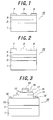
- Fig. 1 is a cross sectional view showing a FET made of a first semiconductor element according to the present invention,
- Fig. 2 is a cross sectional view showing a HEMT made of a second semiconductor element according to the present invention, and
- Fig. 3 is a cross sectional view showing a HBT made of a third semiconductor element.
-
- This invention will be described in detail, hereinafter. Fig. 1 is a cross sectional view showing a FET made of a first semiconductor element according to the present invention. The
FET 10 depicted in Fig. 1 includes asubstrate 1, anunderlayer 2 made of AlN as a first semiconductor nitride epitaxially grown on thesubstrate 1, and aconductive layer 3 made of n-GaN as
a second semiconductor nitride epitaxially grown on theunderlayer 2. In this case, the first semiconductor element is composed of thesubstrate 1, theunderlayer 2 and theconductive layer 3. On theconductive layer 3 are formed asource electrode 7 and adrain electrode 8 having ohmic-contact property and, for example, made of a Ti/Al/Pt/Au multilayered structure. In addition, on theconductive layer 3 is formed agate electrode 9 having ohmic-contact property and, for example, made of a Ni/Pt/Au multilayered structure. - In the
FET 10 depicted in Fig. 1, it is required that the dislocation density of theunderlayer 2 made of AlN is set to 1011/cm2 or below, preferably 1010/cm2 or below. In this case, the dislocation density of theconductive layer 3 made of n-GaN can be reduced to 1010/cm2 or below, preferably 109/cm2 or below, and as a result, the electric properties such as carrier mobility can be enhanced. - It is desired that the dislocation density of the
conductive layer 3 is reduced as low level as possible, and as of now, can be reduced to about 108/cm2. - It is required that the crystallinity of the
underlayer 2 made of AlN is set to 90 seconds or below, preferably 50 seconds or below in FWHM of X-ray rocking curve at (002) reflection. In this case, the crystallinity of theconductive layer 3 can be enhanced to 150 seconds or below, particularly 100 seconds or below in FWHM of X-ray rocking curve at (002) reflection, originated from the higher crystallinity of theunderlayer 2. - The crystallinity and the crystal quality due to low dislocation density can be enhanced, and thus, the electric properties such as mobility in the
conductive layer 3 can be much enhanced. - Such an AIN film as constituting the
underlayer 2 is made by supplying a trimethylaluminum (TMA) and an ammonia (NH3) as raw material gases onto a given substrate heated to preferably 1100°C or over, particularly 1200°C or over. - Conventionally, an underlayer is made of a GaN-based semiconductor not including Al element, and thus, the formation temperature is set to not less than 1000°C and less than 1100°C. On the contrary, the underlayer constituting the semiconductor element of the present invention is made of a nitride including at least Al element, preferably 50 atomic percentages of Al element for all of the III elements of the nitride, and particularly made of AlN as shown in Fig. 1.
- Then, as mentioned above, the underlayer of the semiconductor element of the present invention is preferably made at 1100°C or over, which is very higher than the conventional formation temperature. That is, the underlayer can be made by employing such a quite different condition as the conventional one in a MOCVD method. Herein, the "formation temperature" means "the temperature of the substrate on which the underlayer is formed".
- Although the upper limit value of the formation temperature of the underlayer is not limited, it is preferably set to 1250°C. In this case, the surface roughness of the underlayer due to the material composition thereof can be inhibited, and the diffusion of the components of the underlayer can be also inhibited. As a result, the crystal quality of the underlayer can be developed, irrespective of the material composition of the underlayer, and thus, the crystal quality of the conductive layer can be also developed.
- In view of the enhancement of the crystallinity of the
underlayer 2, it is more preferable as the thickness of the underlayer is increased. However, if theunderlayer 2 is formed too thick, some cracks may be created in theunderlayer 2, and theunderlayer 2 may be broken away from on the substrate. Therefore, it is desired that the thickness of theunderlayer 2 is set to 0.5 µm or over, particularly within 1-3 µm. - The
substrate 1 may be made of oxide single crystal such as sapphire single crystal, ZnO single crystal, LiAlO2 single crystal, LiGaO2 single crystal, MgAl2O4 single crystal, or MgO single crystal, IV single crystal or IV-IV single crystal such as Si single crystal or SiC single crystal, III-V single crystal such as GaAs single crystal, AlN single crystal, GaN single crystal or AlGaN single crystal, and boride single crystal such as ZrB2. - Particularly, in the case of making the substrate of the sapphire single crystal, it is desired that surface-nitriding treatment is performed on the main surface for the
underlayer 2. The surface-nitriding treatment is performed as follows. First of all, the sapphire single crystal substrate is set in a nitrogen-including atmosphere such as an ammonia atmosphere, and then, heated for a given period. The thickness of the resulting surface nitride layer can be adjusted by controlling the nitrogen concentration, the nitriding temperature and the nitriding period appropriately. - If the sapphire single crystal substrate having the surface nitriding layer thereon is employed, the crystallity of the
underlayer 2 formed directly on the main surface can be more enhanced. Moreover, since theunderlayer 2 can be easily formed thicker without cracks and breakaway, for example, up to 3 µm of the upper limit value in the above-mentioned preferable thickness range, not by using a specific forming condition, the crystallinity of theunderlayer 2 can be easily more enhanced due to the increase in thickness. As a result, the crystal quality of the underlayer can be much enhanced due to the higher crystallinity originated from the surface nitriding layer. - Consequently, the crystal quality of the
conductive layer 3 formed on theunderlayer 2 can be developed, and thus, the dislocation density of theconductive layer 3 can be more reduced. - In addition, if the sapphire single crystal having the surface nitriding layer is employed. the higher crystal quality of the
underlayer 2 can be maintained even though theunderlayer 2 is made even at 1200°C or below, particularly around 1150°C, within the above-mentioned preferable formation temperature range. Concretely, in this case, the dislocation density of theunderlayer 2 can be easily reduced to 1010/cm2 or below. - It is desired that the surface-nitriding layer is formed thicker, for example, so that the nitrogen content of the sapphire single crystal substrate at the depth of 1 nm from the main surface is set to two atomic percentages or over, in ESCA analysis. Moreover, the surface-nitriding layer may be formed thinner, for example, in a thickness of 1 nm or below.
- In the case of making the underlayer thicker, some tensile stresses may be exerted on the underlayer and thus, some cracks may be created in the underlayer. In this case, it is desired that the material composition is varied continuously or stepwisely from the substrate toward the conductive layer. Thereby, the lattice constant of the underlayer can be matched appropriately to the ones of the conductive layer and the substrate, resulting in the reduction of tensile stress for the underlayer and thus, the inhibition of the creation of cracks.
- For example, as shown in Fig. 1, in the case of making the
conductive layer 3 of n-GaN, theunderlayer 2 is made of AlGaN. Then, the Al content of theunderlayer 2 is decreased from thesubstrate 1 toward theconductive layer 3, and the Ga content of theunderlayer 2 is increased from thesubstrate 1 toward theconductive layer 3. - As shown in Fig. 1, since a SiO2 mask or the like is not included, the
substrate 1, that is, theFET 10 as a semiconductor element can not almost warped. Concretely, in the case that thesubstrate 1 has a diameter of two inches (≒ 5 cm), the warp of the first semiconductor element constituting theFET 10 can be reduced to only 100 µm or below, particularly 50 µm or below. - Fig. 2 is a cross sectional view showing a HEMT made of a second semiconductor element according to the present invention. The same reference numerals are given to the similar constituent portions to the ones of the
FET 10 shown in Fig. 1. - The
HEMT 20 depicted in Fig. 2 includes acarrier moving layer 3 instead of theconductive layer 3 and acarrier supplying layer 4 made of n-AlGaN as a third semiconductor nitride and formed on thecarrier moving layer 3. However, it is required that anunderlayer 2 is formed in the same manner as the one of theFET 10, and thus, the same conditions are required for theunderlayer 2. Thesubstrate 1 may be also made of a single crystal as mentioned above, and in the case of using the sapphire single crystal, the surface-nitriding treatment is preferably performed for the main surface of the sapphire single crystal substrate. In this case, the second semiconductor element is composed of thesubstrate 1, theunderlayer 2, thecarrier moving layer 3 and thecarrier supplying layer 4. Moreover, asource electrode 7, adrain electrode 8 and agate electrode 9 may be made in the same manner as the ones of theFET 10. In theHEMT 20, carriers are supplied into thecarrier moving layer 3 from thecarrier supplying layer 4, and moved in the surface region of thecarrier moving layer 3. - Moreover, in order to inhibit the creation of cracks, it is desired that the material composition of the
underlayer 2 is varied continuously or stepwisely from thesubstrate 1 toward thecarrier moving layer 3. - Then, since a SiO2 mask or the like is not included, the
substrate 1 is not almost warped. Concretely, the warp of the second semiconductor element constituting theHEMT 20 can be reduced to 100 µm or below, particularly 50 µm or below if the diameter of thesubstrate 1 is set to two inches (≒5 cm). - Fig. 3 is a cross sectional view showing a HBT made of a third semiconductor element. The same reference numerals are given to the similar constituent portions to the ones of the
FET 10 shown in Fig. 1. - The
HBT 30 depicted in Fig. 3 includes asubstrate 1, anunderlayer 2 made of AlN as a first semiconductor nitride and epitaxially grown on thesubstrate 1, and a firstconductive layer 13 of a first conduction type made of n-GaN as a second semiconductor nitride. - The
HBT 30 also includes, on the firstconductive layer 13, a secondconductive layer 14 of the first conduction type made of n-GaN as a third semiconductor nitride, and a thirdconductive layer 15 of a second conduction type made of P+-GaN as a fourth semiconductor nitride. Moreover, theHBT 30 includes, on the thirdconductive layer 15, a fourthconductive layer 16 of the first conductive type made of n+-AlGaN as a fifth semiconductor nitride. As a result, theHBT 30 has an npn-type junction structure. In this case, the third semiconductor element is composed of thesubstrate 1, theunderlayer 2, and the first through the fourth conductive layers 13-15. - On the exposed surface of the first
conductive layer 13 is formed acollector electrode 18 made of a Ti/Al/Pt/Au multilayered structure, and on the exposed surface of the thirdconductive layer 15 is formed abase electrode 17 made of a Ni/Pt/Au multilayered structure. On the fourthconductive layer 16 is formed anemitter electrode 19 made of a similar Ti/Al/Pt/Au multilayered structure. - It is required that the
underlayer 2 is formed in the same manner as the one of theFET 10, and thus, the same conditions arc required for theunderlayer 2. As a result, the dislocation densities of the first through the fourth conductive layers can be reduced to 1010/cm2 or below, particularly 109/cm2 or below. Moreover, the crystallinities of the first through the fourth conductive layers can be developed to 90 seconds or below, particularly 50 seconds or below in FWHM of X-ray rocking curve at (002) reflection. Therefore, the crystal qualities of the first through the fourth conductive layers can be enhanced, and thus, the electric properties such as carrier mobility can be enhanced.
Thesubstrate 1 may be also made of a single crystal as mentioned above, and in the case of using the sapphire single crystal, the surface-nitriding treatment is preferably performed for the main surface of the sapphire single crystal substrate. - As mentioned above, in the case that the lattice constant of the
underlayer 2 is largely different from the one of thesubstrate 1 and/or the firstconductive layer 13, it is desired that the material composition of theunderlayer 2 is varied continuously or stepwisely from thesubstrate 1 toward the firstconductive layer 13 in order to inhibit the creation of cracks. Thesubstrate 1 may be made of the same single crystal as mentioned above. - Then, since a SiO2 mask or the like is not included, the
substrate 1 is not almost warped. Concretely, the warp of the third semiconductor element constituting theHBT 30 can be reduced to 100 µm or below, particularly 50 µm or below if the diameter of thesubstrate 1 is set to two inches (≒5 cm). - It is required in the present invention that the semiconductor layers constituting the semiconductor elements such as a FET, a HEMT and a HBT shown in Figs. 1-3 are made of nitrides including at least one element selected from the group consisting of Al, Ga and In. In addition, the nitrides to constitute the semiconductor layers may include an additive element such as Ge, Si, Mg, Zn, Be, P or B as occasion demands, and a minute impurity contained in the raw material gases and the reactor or contained dependent on the forming condition.
- Such a semiconductor element as a FET, a HEMT and a HBT shown in Figs. 1-3 may be fabricated by a conventional method only if the underlayers and the conductive layers are made under the conditions required by the present invention.
- This invention will be concretely described, hereinafter.
- A sapphire single crystal substrate having a diameter of 2 inches and a thickness of 430 µm was employed, and thus, pre-treated by H2SO4+H2O2, and set into a MOCVD apparatus. To the MOCVD apparatus was attached a gas system of H2, N2, TMA, TMG, NH3 and SiH4. Then, the substrate was heated to 1200°C with flowing H2 gas at a rate of 1m/sec. Thereafter, an ammonia gas (NH3) was flown with a H2 carrier gas for five minutes, to nitride the main surface of the substrate. In ESCA analysis, it was turned out that a surface-nitriding layer was formed on the main surface by the surface-nitriding treatment, and the nitrogen content at the depth of 1 nm from the main surface was seven atomic percentages.
- Then, a TMA and a NH3 were flown at an average rate of 10m/sec, to epitaxially grow an AlN film in a thickness of 1 µm as an underlayer.
The dislocation density of the AlN film was 8×10⁹/cm2, and the FWHM in X-ray rocking curve of the AIN film was 90 seconds. As a result, the good crystal quality of the AlN film was confirmed. Moreover, the surface roughness Ra of the AIN film was 2Å within a 5 µm area, and thus, the good surface flatness of the AlN film was also confirmed. - Then, a TMG, a NH3 and a SiH4 were flown at an average rate of 1m/sec, to epitaxially grow a Si-doped n-GaN film as a conductive layer. The dislocation density of the n-GaN film was 2×10⁸/cm2, and the FWHM in X-ray rocking curve of the n-GaN film was 120 seconds at (002) reflection. Moreover, the carrier density of the n-GaN film was 8×10¹⁶/cm3, and the mobility at room temperature was 800cm2/V · sec.
- Then, a source electrode and a drain electrode of a Ti/Al/Pt/Au multilayered structure were fabricated on the n-GaN film, and a gate electrode of a Ni/Pt/Au multilayered structure was fabricated on the n-GaN film. Herein, the gate length and the gate width were set to 0.5 µm and 70 µm, respectively.
- When the high frequency performance of the thus obtained FET was examined, the cut-off frequency ft was 30 GHz. Therefore, it was confirmed that the FET has an extreme high frequency performance.
- After a surface nitriding treatment was carried out for a sapphire substrate in the same manner as Example 1, an AlN film and an i-GaN film were epitaxially grown subsequently, as an underlayer and a carrier moving layer, respectively. The dislocation densities the AlN film and the i-GaN film were 8×10⁹/cm2 and 2×10⁸/cm2, respectively, and the FWHMs in X-ray rocking curve at (002) reflection of the AIN film and the i-GaN film were 90 seconds and 120 seconds, respectively.
- Then, a TMA, a TMG and a NH3 were flown at an average rate of 3m/sec, to epitaxially grow, on the i-GaN film, an n-AlGaN film as a carrier supplying layer.
- Thereafter, a source electrode and a drain electrode of a Ti/Al/Pt/Au multilayered structure were fabricated on the n-AlGaN film, and a gate electrode of a Ni/Pt/Au multilayered structure was fabricated on the n-AlGaN film. Herein, the gate length and the gate width were set to 0.5 µm and 70 µm, respectively.
- The mobility of the thus obtained HEMT at room temperature was 2000cm2/V · sec. When the high frequency performance of the HEMT was examined, the cut-off frequency ft was 60 GHz. Therefore, it was confirmed that the HEMT has an extreme high frequency performance.
- As is apparent from Examples 1 and 2, the FET and the HEMT according to the present invention can have extreme electric properties such as carrier concentration and mobility, and can exhibit extreme high frequency performances. In the other words, the semiconductor element of the present invention can be used as a practical device such as a FET and a HEMT.
- Although the present invention was described in detail with reference to the above examples, this invention is not limited to the above disclosure and every kind of variation and modification may be made without departing from the scope of the present invention. For example, the thickness and the material composition of the semiconductor layer may be appropriately determined. Moreover, the carrier concentration of the conductive layer may be appropriately determined.
- Then, in the
HEMT 20 shown in Fig. 2, an i-AlGaN film may be formed as a spacer to prevent the diffusion of Si element between thecarrier moving layer 3 and thecarrier supplying layer 4. Moreover, an n-GaN film may be formed on thecarrier supplying layer 4 as a contact layer to reduce the electric contact resistances of the electrodes. Furthermore, in order to prevent the diffusion of Si element, a barrier layer may be formed between thecarrier supplying layer 4 and the contact. layer. - In the
HBT 30 shown in Fig. 3, although theHBT 30 has an npn-type junction structure, it may have a pnp-type junction structure by changing the conduction types of the semiconductor layers of theHBT 30. Moreover, for developing the crystal qualities of the conductive layers 13-16 formed on theunderlayer 2, a buffer layer or a multilayered structure such as a distorted superlattice structure may be provided between theunderlayer 2 and theconductive layer 13. - As mentioned above, since the semiconductor element of the present invention has an underlayer of low dislocation density and high crystallinity, and a conductive layer of high crystal quality originated from the underlayer, the electric properties of the semiconductor element can be enhanced. Therefore, the semiconductor element can be used; as a semiconductor device having semiconductor layers including at least one element selected from the group consisting of Al, Ga and In, for a practical device.
- On a substrate is epitaxially grown an AlN film as an underlayer having a dislocation density of 1011/cm2 or below and a crystallinity of 90 seconds or below in full width at half maximum (FWHM) of X-ray rocking curve at (002) reflection. Then, on the AlN film is epitaxially gown an n-GaN film as a conductive layer having a dislocation density of 1010/cm2 or below and a crystallinity of 150 seconds or below in full width at half maximum (FWHM) of X-ray rocking curve at (002) reflection, to fabricate a semiconductor element.
Claims (23)
- A semiconductor element, substantially comprising:a substrate,an underlayer, epitaxially grown on the substrate, made of a first semiconductor nitride including at least Al element, the dislocation density of the underlayer being set to 1011/cm2 or below, the crystallinity of the underlayer being set to 90 seconds or below in full width at half maximum of X-ray rocking curve at (002) reflection, anda conductive layer, epitaxially grown on the underlayer, made of a second semiconductor nitride including at least one element selected from the group consisting of Al, Ga and In, the dislocation of the conductive layer being set to 1010/cm2 or below, the crystallinity of the conductive layer being set to 150 seconds or below in full width at half maximum of X-ray rocking curve at (002) reflection.
- A semiconductor element as defined in claim 1, wherein the Al content of the first semiconductor nitride constituting the underlayer is set to 50 atomic percentages or over for all of the III elements of the first semiconductor nitride.
- A semiconductor element as defined in claim 2, wherein the underlayer is made of AlN.
- A semiconductor element as defined in any one of claims 1-3, wherein the underlayer is formed at 1100°C or over by a MOCVD method.
- A semiconductor element as defined in claim 4, wherein the underlayer is formed at a temperature within 1100-1250°C.
- A semiconductor element as defined in any one of claims 1-6, wherein the substrate is made of a sapphire single crystal having a surface nitride layer on the main surface of the crystal, and the underlayer is formed on the main surface via the surface nitride layer.
- A semiconductor element as defined in any one of claims 1-6, wherein the material composition of the first semiconductor nitride constituting the underlayer is varied continuously or stepwisely from the substrate toward the conductive layer.
- A semiconductor element as defined in any one of claims 1-7, wherein the warp of the semiconductor element is 100 µ m or below per 5 cm length.
- A field-effect transistor comprising a semiconductor element as defined in any one of claims 1-8, a source electrode, a drain electrode and a gate electrode which are provided on the semiconductor element.
- A semiconductor element, substantially comprising:a substrate,an underlayer, epitaxially grown on the substrate, made of a first semiconductor nitride including at least one element selected from the group consisting of Al, Ga and In, the dislocation density of the underlayer being set to 1011/cm2 or below, the crystallinity of the underlayer being set to 90 seconds or below in full width at half maximum of X-ray rocking curve at (002) reflection,a carrier moving layer, epitaxially grown on the underlayer, made of a second semiconductor nitride including at least one element selected from the group consisting of Al, Ga and In, the dislocation of the carrier moving layer being set to 1010/cm2 or below, the crystallinity of the carrier moving layer being set to 150 seconds or below in full width at half maximum of X-ray rocking curve at (002) reflection, anda carrier supplying layer, epitaxially grown on the carrier moving layer, made of a third semiconductor nitride including at least one element selected from the group consisting of Al, Ga and In.
- A semiconductor element as defined in claim 10, wherein the underlayer is formed at 1100°C or over by a MOCVD method.
- A semiconductor element as defined in claim 11, wherein the underlayer is formed at a temperature within 1100-1250°C.
- A semiconductor element as defined in any one of claims 10-12, wherein the substrate is made of a sapphire single crystal having a surface nitride layer on the main surface of the crystal, and the underlayer is formed on the main surface via the surface nitride layer.
- A semiconductor element as defined in any one of claims 10-13, wherein the material composition of the first semiconductor nitride constituting the underlayer is varied continuously or stepwisely from the substrate toward the conductive layer.
- A semiconductor element as defined in any one of claims 10-14, wherein the warp of the semiconductor element is 100 µm or below per 5 cm length.
- A high electron mobility transistor comprising a semiconductor element as defined in claims 10-15, a source electrode, a drain electrode and a gate electrode which are provided on the semiconductor element.
- A semiconductor element, substantially comprising:a substrate,an underlayer, epitaxially grown on the substrate, made of a first semiconductor nitride including at least one element selected from the group consisting of Al, Ga and In, the dislocation density of the underlayer being set to 1011/cm2 or below, the crystallinity of the underlayer being set to 90 seconds or below in full width at half maximum of X-ray rocking curve at (002) reflection,a first conductive layer of a first conduction type, epitaxially grown on the underlayer, made of a second semiconductor nitride including at least one element selected from the group consisting of Al, Ga and In, the dislocation of the first conductive layer being set to 1010/cm2 or below, the crystallinity of the first conductive layer being set to 150 seconds or below in full width at half maximum of X-ray rocking curve at (002) reflection,a second conductive layer of the first conduction type, epitaxially grown on the first conductive layer, made of a third semiconductor nitride including at least one element selected from the group consisting of Al, Ga and In, the dislocation of the second conductive layer being set to 1010/cm2 or below, the crystallinity of the second conductive layer being set to 90 seconds or below in full width at half maximum of X-ray rocking curve at (002) reflection,a third conductive layer of a second conduction type opposite to the first conduction type, epitaxially grown on the second conductive layer, made of a fourth semiconductor nitride including at least one element selected from the group consisting of Al, Ga and In, the dislocation of the third conductive layer being set to 1010/cm2 or below, the crystallinity of the third conductive layer being set to 150 seconds or below in full width at half maximum of X-ray rocking curve at (002) reflection, anda fourth conductive layer of the first conduction type, epitaxially grown on the third conductive layer, made of a fifth semiconductor nitride including at least one element selected from the group consisting of Al, Ga and In, the dislocation of the fourth conductive layer being set to 1010/cm2 or below, the crystallinity of the fourth conductive layer being set to 150 seconds or below in full width at half maximum of X-ray rocking curve at (002) reflection.
- A semiconductor element as defined in claim 17, wherein the underlayer is formed at 1100°C or over by a MOCVD method.
- A semiconductor element as defined in claim 18, wherein the underlayer is formed at a temperature within 1100-1250°C.
- A semiconductor element as defined in any one of claims 17-19, wherein the substrate is made of a sapphire single crystal having a surface nitride layer on the main surface of the crystal, and the underlayer is formed on the main surface via the surface nitride layer.
- A semiconductor element as defined in any one of claims 17-20, wherein the material composition of the first semiconductor nitride constituting the underlayer is varied continuously or stepwisely from the substrate toward the conductive layer.
- A semiconductor element as defined in any one of claims 17-21, wherein the warp of the semiconductor element is 100 µm or below per 5 cm length.
- A heterojunction bipolar transistor comprising a semiconductor element, an emitter electrode, a collector electrode and a base electrode which are provided on the semiconductor element.
Applications Claiming Priority (6)
| Application Number | Priority Date | Filing Date | Title |
|---|---|---|---|
| JP2000373039 | 2000-12-07 | ||
| JP2000373039 | 2000-12-07 | ||
| JP2001153693 | 2001-05-23 | ||
| JP2001153693 | 2001-05-23 | ||
| JP2001267299 | 2001-09-04 | ||
| JP2001267299A JP3836697B2 (en) | 2000-12-07 | 2001-09-04 | Semiconductor element |
Publications (2)
| Publication Number | Publication Date |
|---|---|
| EP1213767A2 true EP1213767A2 (en) | 2002-06-12 |
| EP1213767A3 EP1213767A3 (en) | 2004-04-14 |
Family
ID=27345391
Family Applications (1)
| Application Number | Title | Priority Date | Filing Date |
|---|---|---|---|
| EP01128995A Withdrawn EP1213767A3 (en) | 2000-12-07 | 2001-12-06 | Nitride compound semiconductor element |
Country Status (3)
| Country | Link |
|---|---|
| US (3) | US6583468B2 (en) |
| EP (1) | EP1213767A3 (en) |
| JP (1) | JP3836697B2 (en) |
Cited By (4)
| Publication number | Priority date | Publication date | Assignee | Title |
|---|---|---|---|---|
| US6703649B2 (en) | 2001-05-31 | 2004-03-09 | Ngk Insulators, Ltd. | Semiconductor element |
| EP1431426A2 (en) * | 2002-12-18 | 2004-06-23 | Ngk Insulators, Ltd. | Substrate for epitaxial growth |
| US7183578B2 (en) | 2003-03-26 | 2007-02-27 | Kyocera Corporation | Semiconductor apparatus, method for growing nitride semiconductor and method for producing semiconductor apparatus |
| CN104246980A (en) * | 2012-04-26 | 2014-12-24 | 应用材料公司 | Pvd buffer layers for led fabrication |
Families Citing this family (35)
| Publication number | Priority date | Publication date | Assignee | Title |
|---|---|---|---|---|
| JP4327339B2 (en) * | 2000-07-28 | 2009-09-09 | 独立行政法人物質・材料研究機構 | Semiconductor layer forming substrate and semiconductor device using the same |
| JP3886341B2 (en) * | 2001-05-21 | 2007-02-28 | 日本電気株式会社 | Method for manufacturing gallium nitride crystal substrate and gallium nitride crystal substrate |
| JP3954335B2 (en) * | 2001-06-15 | 2007-08-08 | 日本碍子株式会社 | Group III nitride multilayer film |
| JP4514727B2 (en) * | 2001-12-25 | 2010-07-28 | 日本碍子株式会社 | Group III nitride film manufacturing method, group III nitride film, group III nitride element epitaxial substrate, and group III nitride element |
| KR100484486B1 (en) * | 2002-10-18 | 2005-04-20 | 한국전자통신연구원 | Nitride semiconductor field effect transistor(FET) fabrication method thereof |
| JP2004289005A (en) * | 2003-03-24 | 2004-10-14 | Ngk Insulators Ltd | Epitaxial substrate, semiconductor device, and high electron mobility transistor |
| JP2004327882A (en) * | 2003-04-28 | 2004-11-18 | Ngk Insulators Ltd | Epitaxial substrate, semiconductor device, and high electron-mobility transistor |
| US7078743B2 (en) * | 2003-05-15 | 2006-07-18 | Matsushita Electric Industrial Co., Ltd. | Field effect transistor semiconductor device |
| US7238970B2 (en) * | 2003-10-30 | 2007-07-03 | Matsushita Electric Industrial Co., Ltd. | Semiconductor device and method for fabricating the same |
| JP2005136200A (en) * | 2003-10-30 | 2005-05-26 | Univ Nagoya | Nitride semiconductor crystalline layer, manufacturing method therefor, and substrate for manufacturing the same |
| US6987300B2 (en) * | 2004-03-25 | 2006-01-17 | Microchip Technology Incorporated | High voltage ESD-protection structure |
| US7981744B2 (en) | 2004-06-10 | 2011-07-19 | Toyoda Gosei Co., Ltd. | Field-effect transistor, semiconductor device, a method for manufacturing them, and a method of semiconductor crystal growth |
| JP2006032911A (en) * | 2004-06-15 | 2006-02-02 | Ngk Insulators Ltd | Semiconductor laminated structure, semiconductor device, and hemt element |
| JP4712450B2 (en) * | 2004-06-29 | 2011-06-29 | 日本碍子株式会社 | Method for improving surface flatness of AlN crystal |
| US7339255B2 (en) * | 2004-08-24 | 2008-03-04 | Kabushiki Kaisha Toshiba | Semiconductor device having bidirectionally inclined toward <1-100> and <11-20> relative to {0001} crystal planes |
| CN101189746B (en) | 2005-03-17 | 2011-08-24 | 日本电气株式会社 | Film enclosed electric device and production method therefor |
| JP5135686B2 (en) * | 2005-03-23 | 2013-02-06 | 住友電気工業株式会社 | Group III nitride semiconductor device |
| JP4432827B2 (en) * | 2005-04-26 | 2010-03-17 | 住友電気工業株式会社 | Group III nitride semiconductor device and epitaxial substrate |
| JP4984425B2 (en) * | 2005-04-28 | 2012-07-25 | 住友電気工業株式会社 | Field effect transistor and epitaxial substrate |
| US8853666B2 (en) | 2005-12-28 | 2014-10-07 | Renesas Electronics Corporation | Field effect transistor, and multilayered epitaxial film for use in preparation of field effect transistor |
| JP4670055B2 (en) * | 2006-03-20 | 2011-04-13 | Dowaエレクトロニクス株式会社 | Semiconductor substrate and semiconductor device |
| US7494546B1 (en) * | 2006-07-14 | 2009-02-24 | Blue Wave Semicodnuctors, Inc. | Method of growing insulating, semiconducting, and conducting group III-nitride thin films and coatings, and use as radiation hard coatings for electronics and optoelectronic devices |
| JP5311765B2 (en) * | 2006-09-15 | 2013-10-09 | 住友化学株式会社 | Semiconductor epitaxial crystal substrate and manufacturing method thereof |
| JP4712683B2 (en) * | 2006-12-21 | 2011-06-29 | パナソニック株式会社 | Transistor and manufacturing method thereof |
| JP2008205221A (en) * | 2007-02-20 | 2008-09-04 | Furukawa Electric Co Ltd:The | Semiconductor device |
| US8304809B2 (en) * | 2007-11-16 | 2012-11-06 | Furukawa Electric Co., Ltd. | GaN-based semiconductor device and method of manufacturing the same |
| JP2010206020A (en) | 2009-03-04 | 2010-09-16 | Panasonic Corp | Semiconductor device |
| JP5193150B2 (en) * | 2009-09-24 | 2013-05-08 | 日本電信電話株式会社 | Nitride semiconductor device and manufacturing method thereof |
| JP2012015304A (en) * | 2010-06-30 | 2012-01-19 | Sumitomo Electric Ind Ltd | Semiconductor device |
| JP2012015303A (en) * | 2010-06-30 | 2012-01-19 | Sumitomo Electric Ind Ltd | Semiconductor substrate and semiconductor device |
| JP5455875B2 (en) * | 2010-11-25 | 2014-03-26 | 日本碍子株式会社 | Epitaxial substrate manufacturing method |
| JP2015133354A (en) | 2014-01-09 | 2015-07-23 | 日立金属株式会社 | nitride semiconductor epitaxial wafer and nitride semiconductor device |
| US10636663B2 (en) | 2017-03-29 | 2020-04-28 | Toyoda Gosei Co., Ltd. | Method of manufacturing semiconductor device including implanting impurities into an implanted region of a semiconductor layer and annealing the implanted region |
| CN111164733B (en) * | 2017-07-20 | 2024-03-19 | 斯维甘公司 | Heterostructure for high electron mobility transistor and method of producing the same |
| US12094958B2 (en) * | 2019-12-05 | 2024-09-17 | Enkris Semiconductor, Inc. | Semiconductor structures and manufacturing methods thereof |
Citations (2)
| Publication number | Priority date | Publication date | Assignee | Title |
|---|---|---|---|---|
| WO1998035388A1 (en) | 1995-11-09 | 1998-08-13 | Northrop Grumman Corporation | Aluminium gallium nitride (algan) based heterojunction bipolar transistor |
| EP1211736A2 (en) * | 2000-11-30 | 2002-06-05 | Ngk Insulators, Ltd. | A semiconductor light-emitting element |
Family Cites Families (9)
| Publication number | Priority date | Publication date | Assignee | Title |
|---|---|---|---|---|
| DE69431333T2 (en) * | 1993-10-08 | 2003-07-31 | Mitsubishi Cable Industries, Ltd. | GaN single crystal |
| US5679965A (en) * | 1995-03-29 | 1997-10-21 | North Carolina State University | Integrated heterostructures of Group III-V nitride semiconductor materials including epitaxial ohmic contact, non-nitride buffer layer and methods of fabricating same |
| JPH0964477A (en) * | 1995-08-25 | 1997-03-07 | Toshiba Corp | Semiconductor light emitting element and its manufacture |
| JPH10199896A (en) * | 1997-01-07 | 1998-07-31 | Fujitsu Ltd | Manufacture of semiconductor device and semiconductor device |
| JPH10335637A (en) * | 1997-05-30 | 1998-12-18 | Sony Corp | Hetero-junction field effect transistor |
| JPH11340147A (en) | 1998-05-25 | 1999-12-10 | Matsushita Electron Corp | Manufacture of nitride semiconductor wafer and element |
| TW418549B (en) * | 1998-06-26 | 2001-01-11 | Sharp Kk | Crystal growth method for nitride semiconductor, nitride semiconductor light emitting device, and method for producing the same |
| US6252261B1 (en) * | 1998-09-30 | 2001-06-26 | Nec Corporation | GaN crystal film, a group III element nitride semiconductor wafer and a manufacturing process therefor |
| EP2267784B1 (en) * | 2001-07-24 | 2020-04-29 | Cree, Inc. | INSULATING GATE AlGaN/GaN HEMT |
-
2001
- 2001-09-04 JP JP2001267299A patent/JP3836697B2/en not_active Expired - Lifetime
- 2001-12-04 US US10/007,099 patent/US6583468B2/en not_active Expired - Lifetime
- 2001-12-06 EP EP01128995A patent/EP1213767A3/en not_active Withdrawn
-
2003
- 2003-02-18 US US10/370,350 patent/US6707076B2/en not_active Expired - Lifetime
- 2003-10-21 US US10/690,290 patent/US6781164B2/en not_active Expired - Lifetime
Patent Citations (2)
| Publication number | Priority date | Publication date | Assignee | Title |
|---|---|---|---|---|
| WO1998035388A1 (en) | 1995-11-09 | 1998-08-13 | Northrop Grumman Corporation | Aluminium gallium nitride (algan) based heterojunction bipolar transistor |
| EP1211736A2 (en) * | 2000-11-30 | 2002-06-05 | Ngk Insulators, Ltd. | A semiconductor light-emitting element |
Cited By (6)
| Publication number | Priority date | Publication date | Assignee | Title |
|---|---|---|---|---|
| US6703649B2 (en) | 2001-05-31 | 2004-03-09 | Ngk Insulators, Ltd. | Semiconductor element |
| EP1431426A2 (en) * | 2002-12-18 | 2004-06-23 | Ngk Insulators, Ltd. | Substrate for epitaxial growth |
| EP1431426A3 (en) * | 2002-12-18 | 2006-10-04 | Ngk Insulators, Ltd. | Substrate for epitaxial growth |
| US7183578B2 (en) | 2003-03-26 | 2007-02-27 | Kyocera Corporation | Semiconductor apparatus, method for growing nitride semiconductor and method for producing semiconductor apparatus |
| CN104246980A (en) * | 2012-04-26 | 2014-12-24 | 应用材料公司 | Pvd buffer layers for led fabrication |
| US11011676B2 (en) | 2012-04-26 | 2021-05-18 | Applied Materials, Inc. | PVD buffer layers for LED fabrication |
Also Published As
| Publication number | Publication date |
|---|---|
| US6781164B2 (en) | 2004-08-24 |
| JP2003045899A (en) | 2003-02-14 |
| US6707076B2 (en) | 2004-03-16 |
| EP1213767A3 (en) | 2004-04-14 |
| US20030151065A1 (en) | 2003-08-14 |
| US20040079964A1 (en) | 2004-04-29 |
| JP3836697B2 (en) | 2006-10-25 |
| US6583468B2 (en) | 2003-06-24 |
| US20020113249A1 (en) | 2002-08-22 |
Similar Documents
| Publication | Publication Date | Title |
|---|---|---|
| US6583468B2 (en) | Semiconductor element | |
| EP1875515B1 (en) | Binary group iii-nitride based high electron mobility transistors and methods of fabricating same | |
| US7709859B2 (en) | Cap layers including aluminum nitride for nitride-based transistors | |
| US9166033B2 (en) | Methods of passivating surfaces of wide bandgap semiconductor devices | |
| US6534801B2 (en) | GaN-based high electron mobility transistor | |
| JP4990496B2 (en) | Nitride-based transistor and method of manufacturing the same | |
| US7547928B2 (en) | AlGaN/GaN high electron mobility transistor devices | |
| EP2273553B1 (en) | A method for fabricating AlGaN/GaN HEMT devices | |
| US20070018198A1 (en) | High electron mobility electronic device structures comprising native substrates and methods for making the same | |
| US20060043419A1 (en) | Semiconductor substrate and semiconductor device manufactured by epitaxial growth on the semiconductor substrate | |
| JP2005167275A (en) | Semiconductor device | |
| JP4458223B2 (en) | Compound semiconductor device and manufacturing method thereof | |
| JP2003059948A (en) | Semiconductor device and production method therefor | |
| US6703649B2 (en) | Semiconductor element | |
| KR20150085724A (en) | Nitride semiconductor and method thereof | |
| JP3753068B2 (en) | Method for manufacturing epitaxial wafer for field effect transistor | |
| JP2006114652A (en) | Semiconductor epitaxial wafer and field effect transistor | |
| CN110797394B (en) | Epitaxial structure of high electron mobility transistor and preparation method thereof | |
| JP2006114655A (en) | Semiconductor epitaxial wafer and field effect transistor | |
| JP2004289005A (en) | Epitaxial substrate, semiconductor device, and high electron mobility transistor | |
| JP3987360B2 (en) | Epitaxial substrate, epitaxial substrate for electronic device, and electronic device | |
| JP2000196067A (en) | Nitride iii-v compound semiconductor device | |
| JP2006196557A (en) | Semiconductor epitaxial wafer and field effect transistor | |
| JP2006114653A (en) | Semiconductor epitaxial wafer and field-effect transistor | |
| TW511143B (en) | Method for forming GaN/AlN superlattice structure |
Legal Events
| Date | Code | Title | Description |
|---|---|---|---|
| PUAI | Public reference made under article 153(3) epc to a published international application that has entered the european phase |
Free format text: ORIGINAL CODE: 0009012 |
|
| AK | Designated contracting states |
Kind code of ref document: A2 Designated state(s): AT BE CH CY DE DK ES FI FR GB GR IE IT LI LU MC NL PT SE TR |
|
| AX | Request for extension of the european patent |
Free format text: AL;LT;LV;MK;RO;SI |
|
| PUAL | Search report despatched |
Free format text: ORIGINAL CODE: 0009013 |
|
| RIC1 | Information provided on ipc code assigned before grant |
Ipc: 7H 01L 29/20 A |
|
| AK | Designated contracting states |
Kind code of ref document: A3 Designated state(s): AT BE CH CY DE DK ES FI FR GB GR IE IT LI LU MC NL PT SE TR |
|
| AX | Request for extension of the european patent |
Extension state: AL LT LV MK RO SI |
|
| 17P | Request for examination filed |
Effective date: 20040825 |
|
| AKX | Designation fees paid |
Designated state(s): AT BE CH CY DE DK ES FI FR GB GR IE IT LI LU MC NL PT SE TR |
|
| 17Q | First examination report despatched |
Effective date: 20081114 |
|
| GRAP | Despatch of communication of intention to grant a patent |
Free format text: ORIGINAL CODE: EPIDOSNIGR1 |
|
| RIC1 | Information provided on ipc code assigned before grant |
Ipc: H01L 29/20 20060101AFI20160929BHEP Ipc: H01L 21/02 20060101ALI20160929BHEP Ipc: H01L 29/66 20060101ALI20160929BHEP |
|
| INTG | Intention to grant announced |
Effective date: 20161019 |
|
| STAA | Information on the status of an ep patent application or granted ep patent |
Free format text: STATUS: THE APPLICATION IS DEEMED TO BE WITHDRAWN |
|
| 18D | Application deemed to be withdrawn |
Effective date: 20170301 |