EP1207563A2 - Direct bonding of flip-chip light-emitting diode and flip-chip ESD protection chip to electrodes in a package - Google Patents
Direct bonding of flip-chip light-emitting diode and flip-chip ESD protection chip to electrodes in a package Download PDFInfo
- Publication number
- EP1207563A2 EP1207563A2 EP01204132A EP01204132A EP1207563A2 EP 1207563 A2 EP1207563 A2 EP 1207563A2 EP 01204132 A EP01204132 A EP 01204132A EP 01204132 A EP01204132 A EP 01204132A EP 1207563 A2 EP1207563 A2 EP 1207563A2
- Authority
- EP
- European Patent Office
- Prior art keywords
- flip
- led
- power shunting
- light
- emitting diode
- Prior art date
- Legal status (The legal status is an assumption and is not a legal conclusion. Google has not performed a legal analysis and makes no representation as to the accuracy of the status listed.)
- Withdrawn
Links
Images


Classifications
-
- H—ELECTRICITY
- H10—SEMICONDUCTOR DEVICES; ELECTRIC SOLID-STATE DEVICES NOT OTHERWISE PROVIDED FOR
- H10W—GENERIC PACKAGES, INTERCONNECTIONS, CONNECTORS OR OTHER CONSTRUCTIONAL DETAILS OF DEVICES COVERED BY CLASS H10
- H10W90/00—Package configurations
-
- H—ELECTRICITY
- H05—ELECTRIC TECHNIQUES NOT OTHERWISE PROVIDED FOR
- H05B—ELECTRIC HEATING; ELECTRIC LIGHT SOURCES NOT OTHERWISE PROVIDED FOR; CIRCUIT ARRANGEMENTS FOR ELECTRIC LIGHT SOURCES, IN GENERAL
- H05B45/00—Circuit arrangements for operating light-emitting diodes [LED]
- H05B45/40—Details of LED load circuits
-
- H—ELECTRICITY
- H10—SEMICONDUCTOR DEVICES; ELECTRIC SOLID-STATE DEVICES NOT OTHERWISE PROVIDED FOR
- H10H—INORGANIC LIGHT-EMITTING SEMICONDUCTOR DEVICES HAVING POTENTIAL BARRIERS
- H10H20/00—Individual inorganic light-emitting semiconductor devices having potential barriers, e.g. light-emitting diodes [LED]
- H10H20/80—Constructional details
- H10H20/85—Packages
- H10H20/857—Interconnections, e.g. lead-frames, bond wires or solder balls
-
- H—ELECTRICITY
- H10—SEMICONDUCTOR DEVICES; ELECTRIC SOLID-STATE DEVICES NOT OTHERWISE PROVIDED FOR
- H10W—GENERIC PACKAGES, INTERCONNECTIONS, CONNECTORS OR OTHER CONSTRUCTIONAL DETAILS OF DEVICES COVERED BY CLASS H10
- H10W72/00—Interconnections or connectors in packages
- H10W72/851—Dispositions of multiple connectors or interconnections
- H10W72/874—On different surfaces
- H10W72/884—Die-attach connectors and bond wires
-
- H—ELECTRICITY
- H10—SEMICONDUCTOR DEVICES; ELECTRIC SOLID-STATE DEVICES NOT OTHERWISE PROVIDED FOR
- H10W—GENERIC PACKAGES, INTERCONNECTIONS, CONNECTORS OR OTHER CONSTRUCTIONAL DETAILS OF DEVICES COVERED BY CLASS H10
- H10W74/00—Encapsulations, e.g. protective coatings
-
- H—ELECTRICITY
- H10—SEMICONDUCTOR DEVICES; ELECTRIC SOLID-STATE DEVICES NOT OTHERWISE PROVIDED FOR
- H10W—GENERIC PACKAGES, INTERCONNECTIONS, CONNECTORS OR OTHER CONSTRUCTIONAL DETAILS OF DEVICES COVERED BY CLASS H10
- H10W90/00—Package configurations
- H10W90/701—Package configurations characterised by the relative positions of pads or connectors relative to package parts
- H10W90/731—Package configurations characterised by the relative positions of pads or connectors relative to package parts of die-attach connectors
- H10W90/736—Package configurations characterised by the relative positions of pads or connectors relative to package parts of die-attach connectors between a chip and a stacked lead frame, conducting package substrate or heat sink
-
- H—ELECTRICITY
- H10—SEMICONDUCTOR DEVICES; ELECTRIC SOLID-STATE DEVICES NOT OTHERWISE PROVIDED FOR
- H10W—GENERIC PACKAGES, INTERCONNECTIONS, CONNECTORS OR OTHER CONSTRUCTIONAL DETAILS OF DEVICES COVERED BY CLASS H10
- H10W90/00—Package configurations
- H10W90/701—Package configurations characterised by the relative positions of pads or connectors relative to package parts
- H10W90/751—Package configurations characterised by the relative positions of pads or connectors relative to package parts of bond wires
- H10W90/753—Package configurations characterised by the relative positions of pads or connectors relative to package parts of bond wires between laterally-adjacent chips
-
- H—ELECTRICITY
- H10—SEMICONDUCTOR DEVICES; ELECTRIC SOLID-STATE DEVICES NOT OTHERWISE PROVIDED FOR
- H10W—GENERIC PACKAGES, INTERCONNECTIONS, CONNECTORS OR OTHER CONSTRUCTIONAL DETAILS OF DEVICES COVERED BY CLASS H10
- H10W90/00—Package configurations
- H10W90/701—Package configurations characterised by the relative positions of pads or connectors relative to package parts
- H10W90/751—Package configurations characterised by the relative positions of pads or connectors relative to package parts of bond wires
- H10W90/756—Package configurations characterised by the relative positions of pads or connectors relative to package parts of bond wires between a chip and a stacked lead frame, conducting package substrate or heat sink
-
- Y—GENERAL TAGGING OF NEW TECHNOLOGICAL DEVELOPMENTS; GENERAL TAGGING OF CROSS-SECTIONAL TECHNOLOGIES SPANNING OVER SEVERAL SECTIONS OF THE IPC; TECHNICAL SUBJECTS COVERED BY FORMER USPC CROSS-REFERENCE ART COLLECTIONS [XRACs] AND DIGESTS
- Y02—TECHNOLOGIES OR APPLICATIONS FOR MITIGATION OR ADAPTATION AGAINST CLIMATE CHANGE
- Y02B—CLIMATE CHANGE MITIGATION TECHNOLOGIES RELATED TO BUILDINGS, e.g. HOUSING, HOUSE APPLIANCES OR RELATED END-USER APPLICATIONS
- Y02B20/00—Energy efficient lighting technologies, e.g. halogen lamps or gas discharge lamps
- Y02B20/30—Semiconductor lamps, e.g. solid state lamps [SSL] light emitting diodes [LED] or organic LED [OLED]
Definitions
- This invention relates to light-emitting diodes and, in particular, to electrostatic discharge protection for such light-emitting diodes.
- LEDs Due to their compact size, high reliability and low power consumption, light-emitting diodes (LEDs) have replaced incandescent bulbs in a variety of applications. However, LEDs are susceptible to damage from electrostatic discharge (ESD), which degrades the performance and reliability of the LED.
- ESD electrostatic discharge
- Past attempts to solve these problems have included the incorporation of a power shunting element in the LED package that provides the LED with protection from overvoltages, such as ESD voltages.
- the power shunting element and LED terminals are coupled in parallel within the LED package.
- the power shunting element diverts electrical current from the LED to limit voltage across the LED when a certain voltage across the LED is exceeded.
- An LED assembly incorporating a power shunting element is described in U.S. Patent No. 5,914,501 (the '501 patent) to Hewlett-Packard Company, and that assembly is reproduced in Figure 1.
- the assembly 10a employs a wire 24a to electrically connect one terminal 15 of the LED 14 to a terminal 12a of the power shunting element 12 and employs another wire 24b to electrically connect the terminal 12a to the positive electrode 22b.
- the other terminal 17 of the LED 14 and the other terminal 12b of the power shunting element 12 are directly bonded to the negative electrode 22a.
- a lens 23 encapsulates the assembly.
- FIG. 2 Another LED assembly 10b (Fig. 2) described in the '501 patent incorporates a power shunting element 12 as a submount for the LED 14.
- the assembly employs wires 24a and 24b to electrically connect the terminals of the LED 14 and power shunting element 12 to the positive and negative electrodes.
- a light-emitting diode assembly incorporates a power shunting element to protect against damage from electrical overstress, such as from electrostatic discharge (ESD).
- the power shunting element is coupled in parallel to the LED within the LED lens assembly itself and protects the LED by diverting electrical current from the LED when a certain voltage across the LED is exceeded.
- LED assemblies of the present invention employ direct bonding of the electrical contacts of the LED and the power shunting element to the electrodes of the LED assembly, rather than incorporating wire bonds or submount chips.
- both the LED and the power shunting element are flip-chips having terminals directly bonded to the positive and negative electrodes.
- a lens material may be formed to encapsulate the LED.
- the power shunting element may optionally be encapsulated by the lens material.
- the present invention improves reliability, simplifies manufacturing, and reduces manufacturing costs.
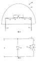
- Figure 3 is a top view of a light-emitting diode package 28 including a light-emitting diode (LED) 30 and a power shunting element 31 arranged according to a first embodiment of the present invention.
- LED light-emitting diode
- the LED 30 and the power shunting element 31 are flip-chips, having terminals on one surface. These terminals are directly bonded to pads 32 and 33 of the respective positive electrode 34 and negative electrode 35.
- the use of flip-chip bonding of both the LED 30 and the power shunting element 31 allows for the complete elimination of wire bonds from the assembly.
- the bonding may be by ultrasonic bonding, adhesive bonding, or soldering.
- flip-chip LED that may be used in the present invention is described in U.S. application serial no. 09/469,657, filed December 22, 1999, entitled III-Nitride Light-Emitting Device With Increased Light Generating Capability, by Michael Krames, Daniel Steigerwald, and others, assigned to the present assignee and incorporated by reference.
- a flip-chip LED includes a transparent substrate on which various active layers are grown or deposited. The electrical contacts are formed on the grown or deposited layers to electrically contact n and p-type layers of the LED. The LED is then mounted such that the substrate is the primary window for the light emission. In Fig. 4, the flip-chip substrate is facing upward.
- a lens 40 encapsulates the LED 30, power shunting element 31, and electrodes 34/35, with extensions 42 and 43 of the electrodes 34 and 35, respectively, protruding from the lens 40 downward from the plane of the page to a circuit board or other apparatus.
- the lens 40 may be a high index epoxy or other material.
- Figure 4 is a side view of the LED package 28 of Figure 3.
- the power shunting element is located behind the LED 30 and is obscured from view.
- the LED 30 terminal 46 is directly bonded to the positive electrode 34.
- the LED 30 terminal 47 is directly bonded to the negative electrode 35.
- the power shunting element has similar terminals directly bonded to the positive electrode 34 and negative electrode 35.
- the heat generated by the LED can be directly extracted by the metal electrodes 34 and 35 serving as heat sinks.
- Figure 5 is an electrical schematic diagram of the LED 30 and the power shunting element 31 in one embodiment of the present invention.
- the back-to-back zener diodes 46 and 47 clamp the voltage across the LED 30 to a predetermined voltage and divert current away from the LED 30.
- the power shunting element 31 protects the LED from electrical overstress, such as that produced by electrostatic discharge.
- the power shunting element may be any transient voltage suppressor diode.
- the power shunting element 31 is located outside the lens for increased optical efficiency.
Landscapes
- Led Device Packages (AREA)
Abstract
Description
Claims (12)
- A light-emitting diode package, comprising:a positive electrode;a negative electrode;a light-emitting diode having a first electrical contact directly bonded to said positive electrode and a second electrical contact directly bonded to said negative electrode; anda power shunting element having a third electrical contact directly bonded to the positive electrode and a fourth electrical contact directly bonded to the negative electrode, said power shunting element shunting electrical current from the light-emitting diode when a voltage applied across the light-emitting diode exceeds a predefined threshold voltage.
- The package of claim 1 wherein said diode and power shunting element are flip-chips, wherein said first and third electrical contacts are flip-chip bonded to the positive electrode, and wherein said second and fourth electrical contacts are flip-chip bonded to the negative electrode.
- The package of claim 1 wherein the power shunting element includes a back-to-back zener diode configuration.
- The package of claim 1 wherein the power shunting element includes a transient voltage suppressor.
- The package of claim 1 further comprising a lens encapsulating said diode and said power shunting element.
- The package of claim 5 wherein said lens is epoxy.
- The package of claim 5 wherein said diode and power shunting elements are flip-chips, wherein said first and third electrical contacts are flip-chip bonded to the positive electrode, and wherein said second and fourth electrical contacts are flip-chip bonded to the negative electrode.
- The package of claim 5 wherein the power shunting element includes a back-to-back zener diode configuration.
- A method for manufacturing a light-emitting diode package comprising:directly bonding a first terminal of a light-emitting diode to a positive electrode and directly bonding a second terminal of said light emitting diode to a negative electrode; anddirectly bonding a third terminal of a power shunting element to the positive electrode and directly bonding a fourth terminal of said power shunting element to the negative electrode, said power shunting element for shunting electrical current from the light-emitting diode when a voltage applied across the light-emitting diode exceeds a predefined threshold voltage.
- The method of claim 9 further comprising encapsulating said diode, said power shunting element, said positive electrode, and said negative electrode with a material to form a lens.
- The method of claim 9 wherein said diode and power shunting element are flip-chips, and said steps of directly bonding comprise flip-chip bonding said first and third electrical contacts to the positive electrode, and flip-chip bonding said second and fourth electrical contacts to the negative electrode.
- The method of claim 9 wherein the power shunting element includes a back-to-back zener diode configuration.
Applications Claiming Priority (2)
| Application Number | Priority Date | Filing Date | Title |
|---|---|---|---|
| US70915000A | 2000-11-08 | 2000-11-08 | |
| US709150 | 2000-11-08 |
Publications (2)
| Publication Number | Publication Date |
|---|---|
| EP1207563A2 true EP1207563A2 (en) | 2002-05-22 |
| EP1207563A3 EP1207563A3 (en) | 2007-03-21 |
Family
ID=24848682
Family Applications (1)
| Application Number | Title | Priority Date | Filing Date |
|---|---|---|---|
| EP01204132A Withdrawn EP1207563A3 (en) | 2000-11-08 | 2001-10-29 | Direct bonding of flip-chip light-emitting diode and flip-chip ESD protection chip to electrodes in a package |
Country Status (3)
| Country | Link |
|---|---|
| EP (1) | EP1207563A3 (en) |
| JP (1) | JP2002185049A (en) |
| KR (1) | KR20020035789A (en) |
Cited By (8)
| Publication number | Priority date | Publication date | Assignee | Title |
|---|---|---|---|---|
| CN100369275C (en) * | 2004-01-29 | 2008-02-13 | 光磊科技股份有限公司 | Light-emitting element capable of increasing light-emitting active region area |
| CN100368895C (en) * | 2006-05-30 | 2008-02-13 | 友达光电股份有限公司 | Backlight module using light emitting diode |
| EP2194761A1 (en) * | 2008-12-03 | 2010-06-09 | Panasonic Electric Works Co., Ltd. | LED Lighting device |
| WO2012151748A1 (en) | 2011-05-11 | 2012-11-15 | 上舜照明(中国)有限公司 | Led chip unit and manufacturing method thereof, and led module |
| US9130365B2 (en) | 2012-03-14 | 2015-09-08 | General Electric Company | Method and system for ultra miniaturized packages for transient voltage suppressors |
| US9343446B2 (en) | 2011-06-08 | 2016-05-17 | Koninklijke Philips N.V. | Diode lighting arrangement |
| US11796163B2 (en) | 2020-05-12 | 2023-10-24 | Feit Electric Company, Inc. | Light emitting device having improved illumination and manufacturing flexibility |
| US11876042B2 (en) | 2020-08-03 | 2024-01-16 | Feit Electric Company, Inc. | Omnidirectional flexible light emitting device |
Families Citing this family (2)
| Publication number | Priority date | Publication date | Assignee | Title |
|---|---|---|---|---|
| CN100392885C (en) * | 2005-08-18 | 2008-06-04 | 璨圆光电股份有限公司 | LED structure |
| KR100795179B1 (en) | 2006-05-30 | 2008-01-16 | 삼성전기주식회사 | Nitride semiconductor light emitting device |
Family Cites Families (4)
| Publication number | Priority date | Publication date | Assignee | Title |
|---|---|---|---|---|
| JPH0725060A (en) * | 1993-06-25 | 1995-01-27 | Matsushita Electric Ind Co Ltd | Optical print head and manufacturing method thereof |
| JP3911839B2 (en) * | 1998-04-08 | 2007-05-09 | 松下電器産業株式会社 | Semiconductor light emitting device |
| JP2000012913A (en) * | 1998-06-19 | 2000-01-14 | Matsushita Electron Corp | Electrostatic protection diode used for semiconductor light emitting device and method of manufacturing the same |
| JP4296644B2 (en) * | 1999-01-29 | 2009-07-15 | 豊田合成株式会社 | Light emitting diode |
-
2001
- 2001-10-17 JP JP2001319159A patent/JP2002185049A/en active Pending
- 2001-10-29 EP EP01204132A patent/EP1207563A3/en not_active Withdrawn
- 2001-11-08 KR KR1020010069349A patent/KR20020035789A/en not_active Ceased
Cited By (10)
| Publication number | Priority date | Publication date | Assignee | Title |
|---|---|---|---|---|
| CN100369275C (en) * | 2004-01-29 | 2008-02-13 | 光磊科技股份有限公司 | Light-emitting element capable of increasing light-emitting active region area |
| CN100368895C (en) * | 2006-05-30 | 2008-02-13 | 友达光电股份有限公司 | Backlight module using light emitting diode |
| EP2194761A1 (en) * | 2008-12-03 | 2010-06-09 | Panasonic Electric Works Co., Ltd. | LED Lighting device |
| WO2012151748A1 (en) | 2011-05-11 | 2012-11-15 | 上舜照明(中国)有限公司 | Led chip unit and manufacturing method thereof, and led module |
| US9343446B2 (en) | 2011-06-08 | 2016-05-17 | Koninklijke Philips N.V. | Diode lighting arrangement |
| US9130365B2 (en) | 2012-03-14 | 2015-09-08 | General Electric Company | Method and system for ultra miniaturized packages for transient voltage suppressors |
| US11796163B2 (en) | 2020-05-12 | 2023-10-24 | Feit Electric Company, Inc. | Light emitting device having improved illumination and manufacturing flexibility |
| US12066173B2 (en) | 2020-05-12 | 2024-08-20 | Feit Electric Company, Inc. | Light emitting device having improved illumination and manufacturing flexibility |
| US11876042B2 (en) | 2020-08-03 | 2024-01-16 | Feit Electric Company, Inc. | Omnidirectional flexible light emitting device |
| US12293965B2 (en) | 2020-08-03 | 2025-05-06 | Feit Electric Company, Inc. | Omnidirectional flexible light emitting device |
Also Published As
| Publication number | Publication date |
|---|---|
| EP1207563A3 (en) | 2007-03-21 |
| JP2002185049A (en) | 2002-06-28 |
| KR20020035789A (en) | 2002-05-15 |
Similar Documents
| Publication | Publication Date | Title |
|---|---|---|
| KR100650191B1 (en) | High brightness LEDs with built-in protection against electrostatic discharge shock | |
| US7768754B2 (en) | Ceramic substrate for light emitting diode where the substrate incorporates ESD protection | |
| KR100686416B1 (en) | Manufacturing method of composite light emitting device, semiconductor light emitting device and semiconductor light emitting device | |
| TWI389287B (en) | Light-emitting diode chip with integrated body fast switching diode for electrostatic discharge protection | |
| US7683396B2 (en) | High power light emitting device assembly utilizing ESD protective means sandwiched between dual sub-mounts | |
| JP3673621B2 (en) | Chip light emitting device | |
| KR20000017513A (en) | Light emitting diode assembly having integrated electrostatic discharge protection | |
| US7078738B2 (en) | Light-emitting device | |
| JP3559435B2 (en) | Semiconductor light emitting device | |
| JP2001015815A (en) | Semiconductor light emitting device | |
| US20150108533A1 (en) | Light-emitting device | |
| KR100562488B1 (en) | Semiconductor light emitting device | |
| EP1207563A2 (en) | Direct bonding of flip-chip light-emitting diode and flip-chip ESD protection chip to electrodes in a package | |
| JP3348843B2 (en) | Light emitting diode and dot matrix display using the same | |
| US9070614B2 (en) | Semiconductor device and manufacturing method thereof | |
| KR100769720B1 (en) | High brightness LEDs with built-in protection against electrostatic discharge shock | |
| JP3787220B2 (en) | Chip light emitting device | |
| JP2000216442A (en) | Semiconductor light emitting device | |
| JP3789428B2 (en) | Light emitting device | |
| KR100674857B1 (en) | LED package with reinforced electrostatic discharge (ESD) and its manufacturing method | |
| CN212412079U (en) | Light emitting diode packaging structure capable of emitting light laterally | |
| JP3723328B2 (en) | Semiconductor light emitting device | |
| KR100748241B1 (en) | High brightness LEDs with built-in protection against electrostatic discharge shock and manufacturing method | |
| JPH11220176A (en) | Semiconductor light emitting device | |
| KR20160128516A (en) | Semiconductor light emitting device package |
Legal Events
| Date | Code | Title | Description |
|---|---|---|---|
| PUAI | Public reference made under article 153(3) epc to a published international application that has entered the european phase |
Free format text: ORIGINAL CODE: 0009012 |
|
| AX | Request for extension of the european patent |
Free format text: AL;LT;LV;MK;RO;SI |
|
| PUAL | Search report despatched |
Free format text: ORIGINAL CODE: 0009013 |
|
| AK | Designated contracting states |
Kind code of ref document: A3 Designated state(s): AT BE CH CY DE DK ES FI FR GB GR IE IT LI LU MC NL PT SE TR |
|
| AX | Request for extension of the european patent |
Extension state: AL LT LV MK RO SI |
|
| 17P | Request for examination filed |
Effective date: 20070921 |
|
| AKX | Designation fees paid |
Designated state(s): DE GB |
|
| 17Q | First examination report despatched |
Effective date: 20071106 |
|
| RAP1 | Party data changed (applicant data changed or rights of an application transferred) |
Owner name: PHILIPS LUMILEDS LIGHTING COMPANY LLC |
|
| STAA | Information on the status of an ep patent application or granted ep patent |
Free format text: STATUS: THE APPLICATION IS DEEMED TO BE WITHDRAWN |
|
| 18D | Application deemed to be withdrawn |
Effective date: 20140501 |