EP1205967B1 - Verfahren zur Ionenstrahlbearbeitung mit Wasserdampf - Google Patents
Verfahren zur Ionenstrahlbearbeitung mit Wasserdampf Download PDFInfo
- Publication number
- EP1205967B1 EP1205967B1 EP01130911A EP01130911A EP1205967B1 EP 1205967 B1 EP1205967 B1 EP 1205967B1 EP 01130911 A EP01130911 A EP 01130911A EP 01130911 A EP01130911 A EP 01130911A EP 1205967 B1 EP1205967 B1 EP 1205967B1
- Authority
- EP
- European Patent Office
- Prior art keywords
- sputtering
- carbonaceous material
- polyimide
- water vapour
- ion beam
- Prior art date
- Legal status (The legal status is an assumption and is not a legal conclusion. Google has not performed a legal analysis and makes no representation as to the accuracy of the status listed.)
- Expired - Lifetime
Links
Images

Classifications
-
- H10P50/286—
-
- H—ELECTRICITY
- H01—ELECTRIC ELEMENTS
- H01L—SEMICONDUCTOR DEVICES NOT COVERED BY CLASS H10
- H01L21/00—Processes or apparatus adapted for the manufacture or treatment of semiconductor or solid state devices or of parts thereof
- H01L21/02—Manufacture or treatment of semiconductor devices or of parts thereof
- H01L21/04—Manufacture or treatment of semiconductor devices or of parts thereof the devices having potential barriers, e.g. a PN junction, depletion layer or carrier concentration layer
- H01L21/18—Manufacture or treatment of semiconductor devices or of parts thereof the devices having potential barriers, e.g. a PN junction, depletion layer or carrier concentration layer the devices having semiconductor bodies comprising elements of Group IV of the Periodic Table or AIIIBV compounds with or without impurities, e.g. doping materials
- H01L21/30—Treatment of semiconductor bodies using processes or apparatus not provided for in groups H01L21/20 - H01L21/26
- H01L21/31—Treatment of semiconductor bodies using processes or apparatus not provided for in groups H01L21/20 - H01L21/26 to form insulating layers thereon, e.g. for masking or by using photolithographic techniques; After treatment of these layers; Selection of materials for these layers
- H01L21/3105—After-treatment
- H01L21/311—Etching the insulating layers by chemical or physical means
- H01L21/31127—Etching organic layers
-
- H—ELECTRICITY
- H01—ELECTRIC ELEMENTS
- H01J—ELECTRIC DISCHARGE TUBES OR DISCHARGE LAMPS
- H01J37/00—Discharge tubes with provision for introducing objects or material to be exposed to the discharge, e.g. for the purpose of examination or processing thereof
- H01J37/30—Electron-beam or ion-beam tubes for localised treatment of objects
- H01J37/305—Electron-beam or ion-beam tubes for localised treatment of objects for casting, melting, evaporating, or etching
- H01J37/3053—Electron-beam or ion-beam tubes for localised treatment of objects for casting, melting, evaporating, or etching for evaporating or etching
- H01J37/3056—Electron-beam or ion-beam tubes for localised treatment of objects for casting, melting, evaporating, or etching for evaporating or etching for microworking, e. g. etching of gratings or trimming of electrical components
-
- H—ELECTRICITY
- H01—ELECTRIC ELEMENTS
- H01L—SEMICONDUCTOR DEVICES NOT COVERED BY CLASS H10
- H01L21/00—Processes or apparatus adapted for the manufacture or treatment of semiconductor or solid state devices or of parts thereof
- H01L21/02—Manufacture or treatment of semiconductor devices or of parts thereof
- H01L21/04—Manufacture or treatment of semiconductor devices or of parts thereof the devices having potential barriers, e.g. a PN junction, depletion layer or carrier concentration layer
- H01L21/18—Manufacture or treatment of semiconductor devices or of parts thereof the devices having potential barriers, e.g. a PN junction, depletion layer or carrier concentration layer the devices having semiconductor bodies comprising elements of Group IV of the Periodic Table or AIIIBV compounds with or without impurities, e.g. doping materials
- H01L21/30—Treatment of semiconductor bodies using processes or apparatus not provided for in groups H01L21/20 - H01L21/26
- H01L21/302—Treatment of semiconductor bodies using processes or apparatus not provided for in groups H01L21/20 - H01L21/26 to change their surface-physical characteristics or shape, e.g. etching, polishing, cutting
- H01L21/306—Chemical or electrical treatment, e.g. electrolytic etching
- H01L21/3065—Plasma etching; Reactive-ion etching
-
- H—ELECTRICITY
- H01—ELECTRIC ELEMENTS
- H01L—SEMICONDUCTOR DEVICES NOT COVERED BY CLASS H10
- H01L21/00—Processes or apparatus adapted for the manufacture or treatment of semiconductor or solid state devices or of parts thereof
- H01L21/02—Manufacture or treatment of semiconductor devices or of parts thereof
- H01L21/04—Manufacture or treatment of semiconductor devices or of parts thereof the devices having potential barriers, e.g. a PN junction, depletion layer or carrier concentration layer
- H01L21/18—Manufacture or treatment of semiconductor devices or of parts thereof the devices having potential barriers, e.g. a PN junction, depletion layer or carrier concentration layer the devices having semiconductor bodies comprising elements of Group IV of the Periodic Table or AIIIBV compounds with or without impurities, e.g. doping materials
- H01L21/30—Treatment of semiconductor bodies using processes or apparatus not provided for in groups H01L21/20 - H01L21/26
- H01L21/31—Treatment of semiconductor bodies using processes or apparatus not provided for in groups H01L21/20 - H01L21/26 to form insulating layers thereon, e.g. for masking or by using photolithographic techniques; After treatment of these layers; Selection of materials for these layers
- H01L21/3105—After-treatment
- H01L21/311—Etching the insulating layers by chemical or physical means
- H01L21/31127—Etching organic layers
- H01L21/31133—Etching organic layers by chemical means
- H01L21/31138—Etching organic layers by chemical means by dry-etching
-
- H—ELECTRICITY
- H01—ELECTRIC ELEMENTS
- H01L—SEMICONDUCTOR DEVICES NOT COVERED BY CLASS H10
- H01L21/00—Processes or apparatus adapted for the manufacture or treatment of semiconductor or solid state devices or of parts thereof
- H01L21/02—Manufacture or treatment of semiconductor devices or of parts thereof
- H01L21/04—Manufacture or treatment of semiconductor devices or of parts thereof the devices having potential barriers, e.g. a PN junction, depletion layer or carrier concentration layer
- H01L21/18—Manufacture or treatment of semiconductor devices or of parts thereof the devices having potential barriers, e.g. a PN junction, depletion layer or carrier concentration layer the devices having semiconductor bodies comprising elements of Group IV of the Periodic Table or AIIIBV compounds with or without impurities, e.g. doping materials
- H01L21/30—Treatment of semiconductor bodies using processes or apparatus not provided for in groups H01L21/20 - H01L21/26
- H01L21/31—Treatment of semiconductor bodies using processes or apparatus not provided for in groups H01L21/20 - H01L21/26 to form insulating layers thereon, e.g. for masking or by using photolithographic techniques; After treatment of these layers; Selection of materials for these layers
- H01L21/3205—Deposition of non-insulating-, e.g. conductive- or resistive-, layers on insulating layers; After-treatment of these layers
- H01L21/321—After treatment
- H01L21/3213—Physical or chemical etching of the layers, e.g. to produce a patterned layer from a pre-deposited extensive layer
- H01L21/32131—Physical or chemical etching of the layers, e.g. to produce a patterned layer from a pre-deposited extensive layer by physical means only
-
- H10P50/242—
-
- H10P50/262—
-
- H10P50/287—
-
- H—ELECTRICITY
- H01—ELECTRIC ELEMENTS
- H01J—ELECTRIC DISCHARGE TUBES OR DISCHARGE LAMPS
- H01J2237/00—Discharge tubes exposing object to beam, e.g. for analysis treatment, etching, imaging
- H01J2237/30—Electron or ion beam tubes for processing objects
- H01J2237/317—Processing objects on a microscale
- H01J2237/3174—Etching microareas
- H01J2237/31742—Etching microareas for repairing masks
- H01J2237/31744—Etching microareas for repairing masks introducing gas in vicinity of workpiece
Definitions
- the present invention relates to particle beam machining, and, more particularly, to a method for chemically enhancing particle beam machining.
- Focused ion beams are used in forming, shaping, or altering microscopic structures, such as semiconductor devices. See for example, " Scientific American", January 1991, pages 96-101 by Jon Orloff .
- a focused ion beam can be directed to a very small point on a semiconductor device and then scanned, raster fashion, over a surface where material is to be removed. When an ion impinges the surface, its momentum is transferred, resulting in the removal of one or more surface atoms according to a process called sputtering.
- sputtering By selecting a raster pattern of a particular shape, a correspondingly shaped area of surface material can be removed. Often several successive layers of a semiconductor device are removed in a given area in order to expose and possibly sever an underlying layer.
- the material removal rate, or yield volume of material removed per incident ion or other changed particle
- sputtering-enhancing gases typically halogen-based compounds
- the sputter-enhancing gases are relatively stable, except in the area of the workpiece being sputtered, where they react with the workpiece and change the material removal rate from that achieved by physical sputtering alone.
- chemically-enhanced sputtering In addition to increasing yield, chemically-enhanced sputtering also reduces the re-deposition of previously removed material. Furthermore, chemically-enhanced sputtering causes the yield of some materials to increase while not affecting the yield or actually decreasing the yield, of other materials, creating a ratio of yields between those materials.
- the ratio of yields between different materials is referred to as "selectivity", and can be either advantageous or disadvantageous, depending on the situation.
- selectivity the ratio of yields between different materials.
- the process would be simplified dramatically by using a gas which increases the yield of L1 or decreases the yield of L2.
- Such a gas would reduce the processing time required and decrease the criticality of end point detection by increasing the time, relative to the total process time, that L2 can be sputtered without significant removal.
- the document US-A-4,319,889 discloses a method that utilizes an electron beam for the ionization of hydrogen molecules that then react with carbon on a diamond substrate. It also discloses sputtering of a diamond with an ion beam. From WO-A-89/04052 it is known to use water vapour to reduce the effect of the ion beam by reducing its energy therby shortening the penetration depth of implanted ions, reducing radiation damage of the substrate and producing chemical reactions that reduce the staining of the substrate.
- the particle beam may comprise various types of ions including, but not limited to gallium ions.
- the application of the water vapour to the material to be removed may be accomplished by gas jet injecting.
- layers of a first material overlying a second material may be substantially completely removed from the substrate, while the second material is substantially not removed from the substrate.
- layers of polyimide may be removed to expose underlying aluminum interconnects, without removing or damaging the aluminum interconnects.
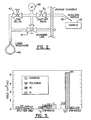
- An evacuated envelope 10 includes an upper neck portion 12 within which a liquid metal ion source 14 and a focusing column 16 are located.
- the particle beam 18 passes from the source 14 through the column 16 and between electrostatic deflectors 20 toward workpiece 22, which is positioned on a movable X-Y stage 24 within the lower chamber 26.
- the workpiece 22 can be any device or substance capable of being machined by a charged particle beam, including, but not limited to, microelectronics including semiconductors, optics and any device having multi-layer coatings.
- An ion pump 28 is employed for evacuating the neck portion 12.
- the lower chamber 26 is evacuated with a pumping system 30 operated by a vacuum controller 32.
- a high voltage power supply 34 is connected to the liquid metal ion source 14 as well as to electrodes (not shown) contained within the focusing column 16 for forming an approximately 25keV particle beam 18 and directing the beam downwardly in the direction of the workpiece 22.
- the deflection controller and amplifier 36 which is operated in accordance with a prescribed pattern such as a raster pattern provided by the pattern generator 38, is coupled to the electrostatic deflection means 20, whereby the particle beam 18 can be controlled to sputter a pattern on the upper surface of the workpiece 22.
- the liquid metal ion source 14 provides a beam of gallium ions, although other ions could be used.
- the focused particle beam system is further provided with a source 46 for supplying water vapour.
- the water vapour is provided via a gas injection system, schematically illustrated in FIG. 2 , and comprises a liquid reservoir 49, injection needle 50, leak valve 47, and shut-off valves 51.
- the water vapour is fed to the surface of the workpiece 22 through an injection needle 50 that is preferably positionable to within approximately 100 ⁇ m of the workpiece.
- the gas flow from the water vapour source 46 may be controlled, for example, using a variable leak valve 47, such as a Granville Phillips Series 203 valve, as would be known to those skilled in the art.
- the gas pressure at the entrance to the injector needle 50 may be monitored using a suitable vacuum gauge 48.
- a desirable flow rate through the needle would be approximately 2.6 x 10 -4 Pa-Litre/s (2 x 10 -6 torr-litre/s), yielding a pressure at the workpiece surface of approximately 0.13 Pa (1 mTorr), although, as would be understood by those having skill in the art, other flow rates and pressures at the surface of the workpiece 22 would be acceptable.
- FIG.3 The removal rates of various materials according to one embodiment of the present invention are illustrated in FIG.3 .
- the yields summarized are for diamond, polyimide, silicon (Si) and aluminum (Al) without any chemical enhancement, with I 2 , enhancement (cited for comparison purposes), and with H 2 0 enhancement.
- Water vapour was introduced to the workpiece surface while a 125 ⁇ m 2 area was scanned with a 1 nanoampere, 25keV gallium ion beam.
- the gallium beam having an approximate diameter of 0.16 of ⁇ m, was scanned in a meander pattern, stepping in 0.16 ⁇ m increments (0% overlap) and dwelling for 0.4 ⁇ s at each step to yield a frame time (time between consecutive exposures of the same pixel) of 2ms.
- the yield ( ⁇ m 3 /nanocoulomb) was measured as the depth milled into the workpiece (determined by cross sectional analysis) divided by the dose of gallium. Yields, both with and without H 2 O enhancement, were measured on polyimide passivation, polymethylmethacrylate (PMMA) resist, Al interconnects, Si and diamond to determine the ratio of yields with and without H 2 O. The ratio of yields using I, was also measured for comparison.
- FIG.3 Two results from H 2 O enhanced sputtering are illustrated in FIG.3 .
- the yields of diamond and polyimide increased by a factor of 7 and 20, respectively, when H 2 O is present.
- the yield achieved for polyimide corresponds to a removal of more than 100 workpiece atoms for each incident ion.
- the amount of Si and Al sputtered from the workpiece decreased by nearly an order of magnitude.
- This combination of increasing the yield of polyimide while decreasing the yield of Si or Al results in a net selectivity to polyimide over Si or Al of more than 400:1, allowing highly material selective machining to be achieved. Accordingly, the present invention allows greater selectivity and control over the rate of removal of more materials than was previously possible.
- Water vapor enhanced particle beam machining not only reduces processing time, but also provides better process control.
- the high selectivity of H 2 O enhanced particle beam machining of polyimide over Al also allows the removal of polyimide passivation and dielectric layers from an integrated circuit to expose multiple metal levels without compromising the integrity of the upper level circuitry. This process would be difficult without H 2 O enhancement. For example, sputtering a 30 x 30 ⁇ m hole, using a 1 nanoampere beam through 6 ⁇ m of polyimide to expose the substrate below takes only 11 minutes. Creating the same hole using physical sputtering alone, takes about 225 minutes, and the upper level Al lines would be completely removed by the time the polyimide dielectric layer had been sputtered from the lower level metal.
- H 2 O enhanced particle beam machining allows PMMA and various other optical resists on Si substrates to be rapidly modified without significant damage to the substrate. This is particularly useful for cross sectional analysis of resist lines and for modification of X-ray masks as it has allowed the resist pattern to be altered, prior to deposition of the absorber metal, without damaging the supporting membrane material.
- the significant increase in the yield for single crystal diamond, from approximately 0.12 to 0.9 ⁇ m 3 /nanocoulomb, when using H 2 O enhanced sputtering greatly increases the capability to micromachine diamond.
Landscapes
- Engineering & Computer Science (AREA)
- Physics & Mathematics (AREA)
- Condensed Matter Physics & Semiconductors (AREA)
- General Physics & Mathematics (AREA)
- Manufacturing & Machinery (AREA)
- Computer Hardware Design (AREA)
- Microelectronics & Electronic Packaging (AREA)
- Power Engineering (AREA)
- Plasma & Fusion (AREA)
- Chemical & Material Sciences (AREA)
- Analytical Chemistry (AREA)
- Chemical Kinetics & Catalysis (AREA)
- General Chemical & Material Sciences (AREA)
- Drying Of Semiconductors (AREA)
- Formation Of Insulating Films (AREA)
- Physical Vapour Deposition (AREA)
- Internal Circuitry In Semiconductor Integrated Circuit Devices (AREA)
- ing And Chemical Polishing (AREA)
Claims (7)
- Verfahren zur Ionenstrahlbearbeitung eines kohlenstoffhaltigen Materials auf einem zweiten Material, um zumindest Teile des kohlenstoffhaltigen Materials zu entfernen, ohne das zweite Material wesentlich zu entfernen, wobei das Verfahren die folgenden Schritte umfasst:a) Auswählen eines Materials als zweites Material, dessen Entfernungsrate während der Ionenstrahlbearbeitung dadurch verringert wird, dass es Wasserdampf ausgesetzt wird, und Ausführen der folgenden Schritte:b) Halten des zweiten Materials mit dem kohlenstoffhaltigen Material auf diesem in einem Vakuum;c) Beschießen eines Teils des kohlenstoffhaltigen Materials mit einem fokussierten Ionenstrahl; undd) Aussetzen des kohlenstoffhaltigen Materials einer Zufuhr von Wasserdampf während des Ionenstrahlbeschusses.
- Verfahren nach Anspruch 1, wobei das kohlenstoffhaltige Material ein Photoresistmaterial oder eine Passivierungsschicht ist.
- Verfahren nach Anspruch 1 oder 2, wobei das zweite Material ein Substrat einer integrierten Schaltung ist.
- Verfahren nach irgendwelchen vorangehenden Ansprüchen, wobei das zweite Material einen Halbleiter und/oder ein Metall und/oder ein Oxid davon umfasst.
- Verfahren nach einem vorangehenden Anspruch, wobei der Wasserdampf durch Gaseinleitung in die Nähe des Teils des kohlenstoffhaltigen Materials, der beschossen werden soll, geliefert wird.
- Verfahren nach einem vorangehenden Anspruch, wobei der Wasserdampf die Zerstäubung des kohlenstoffhaltigen Materials verstärkt, aber die Zerstäubung des zweiten Materials nicht verstärkt.
- Verfahren nach einem vorangehenden Anspruch, wobei das kohlenstoffhaltige Material Diamant oder PMMA und/oder Polyimid umfasst.
Applications Claiming Priority (3)
| Application Number | Priority Date | Filing Date | Title |
|---|---|---|---|
| US08/421,811 US5958799A (en) | 1995-04-13 | 1995-04-13 | Method for water vapor enhanced charged-particle-beam machining |
| EP96911620A EP0820641B9 (de) | 1995-04-13 | 1996-04-08 | Verfahren für verbesserte wasserdampf-ladungsteilchenstrahlbearbeitung |
| US421811 | 1999-10-20 |
Related Parent Applications (1)
| Application Number | Title | Priority Date | Filing Date |
|---|---|---|---|
| EP96911620A Division EP0820641B9 (de) | 1995-04-13 | 1996-04-08 | Verfahren für verbesserte wasserdampf-ladungsteilchenstrahlbearbeitung |
Publications (3)
| Publication Number | Publication Date |
|---|---|
| EP1205967A2 EP1205967A2 (de) | 2002-05-15 |
| EP1205967A3 EP1205967A3 (de) | 2005-03-02 |
| EP1205967B1 true EP1205967B1 (de) | 2009-07-22 |
Family
ID=23672137
Family Applications (2)
| Application Number | Title | Priority Date | Filing Date |
|---|---|---|---|
| EP01130911A Expired - Lifetime EP1205967B1 (de) | 1995-04-13 | 1996-04-08 | Verfahren zur Ionenstrahlbearbeitung mit Wasserdampf |
| EP96911620A Expired - Lifetime EP0820641B9 (de) | 1995-04-13 | 1996-04-08 | Verfahren für verbesserte wasserdampf-ladungsteilchenstrahlbearbeitung |
Family Applications After (1)
| Application Number | Title | Priority Date | Filing Date |
|---|---|---|---|
| EP96911620A Expired - Lifetime EP0820641B9 (de) | 1995-04-13 | 1996-04-08 | Verfahren für verbesserte wasserdampf-ladungsteilchenstrahlbearbeitung |
Country Status (6)
| Country | Link |
|---|---|
| US (2) | US5958799A (de) |
| EP (2) | EP1205967B1 (de) |
| JP (1) | JP3572081B2 (de) |
| AU (1) | AU5445096A (de) |
| DE (2) | DE69625050T2 (de) |
| WO (1) | WO1996032741A1 (de) |
Families Citing this family (23)
| Publication number | Priority date | Publication date | Assignee | Title |
|---|---|---|---|---|
| US5798529A (en) * | 1996-05-28 | 1998-08-25 | International Business Machines Corporation | Focused ion beam metrology |
| IL124592A (en) | 1997-05-23 | 2002-07-25 | Gersan Ets | Method of marking a gemstone or diamond |
| US6414307B1 (en) | 1999-07-09 | 2002-07-02 | Fei Company | Method and apparatus for enhancing yield of secondary ions |
| US6322672B1 (en) * | 2000-03-10 | 2001-11-27 | Fei Company | Method and apparatus for milling copper interconnects in a charged particle beam system |
| US6407001B1 (en) | 2000-06-30 | 2002-06-18 | Intel Corporation | Focused ion beam etching of copper |
| US6514866B2 (en) * | 2001-01-12 | 2003-02-04 | North Carolina State University | Chemically enhanced focused ion beam micro-machining of copper |
| CN1550037A (zh) * | 2001-08-27 | 2004-11-24 | ����̩˹���������ι�˾ | 用带电粒子束微细加工铜的方法 |
| US20030062126A1 (en) * | 2001-10-03 | 2003-04-03 | Scaggs Michael J. | Method and apparatus for assisting laser material processing |
| US7140812B2 (en) * | 2002-05-29 | 2006-11-28 | 3M Innovative Properties Company | Diamond tool with a multi-tipped diamond |
| US20040045419A1 (en) * | 2002-09-10 | 2004-03-11 | Bryan William J. | Multi-diamond cutting tool assembly for creating microreplication tools |
| US6863787B2 (en) * | 2003-04-02 | 2005-03-08 | Fei Company | Dummy copper deprocessing |
| US7060196B2 (en) * | 2003-10-03 | 2006-06-13 | Credence Systems Corporation | FIB milling of copper over organic dielectrics |
| KR101609400B1 (ko) | 2008-04-02 | 2016-04-05 | 쓰리엠 이노베이티브 프로퍼티즈 컴파니 | 광 지향 필름 또는 광 지향 물품 |
| NL2004888A (en) * | 2009-06-29 | 2010-12-30 | Asml Netherlands Bv | Deposition method and apparatus. |
| US9136794B2 (en) | 2011-06-22 | 2015-09-15 | Research Triangle Institute, International | Bipolar microelectronic device |
| US9443697B2 (en) * | 2012-01-31 | 2016-09-13 | Fei Company | Low energy ion beam etch |
| US9275823B2 (en) | 2012-03-21 | 2016-03-01 | Fei Company | Multiple gas injection system |
| US9001463B2 (en) | 2012-08-31 | 2015-04-07 | International Business Machines Corporaton | Magnetic recording head having protected reader sensors and near zero recessed write poles |
| US9349395B2 (en) * | 2012-08-31 | 2016-05-24 | International Business Machines Corporation | System and method for differential etching |
| EP2787523B1 (de) * | 2013-04-03 | 2016-02-10 | Fei Company | Niedrigenergieionendünnung oder -abscheidung |
| US10347463B2 (en) | 2016-12-09 | 2019-07-09 | Fei Company | Enhanced charged particle beam processes for carbon removal |
| US11894213B2 (en) | 2018-06-22 | 2024-02-06 | Hitachi High-Tech Corporation | Ion milling device |
| CZ202363A3 (cs) | 2023-02-19 | 2024-10-09 | Tescan Group, A.S. | Zařízení s fokusovaným svazkem nabitých částic a způsob opracování či zobrazování vzorků |
Family Cites Families (29)
| Publication number | Priority date | Publication date | Assignee | Title |
|---|---|---|---|---|
| US3548189A (en) * | 1965-06-16 | 1970-12-15 | Aden B Meinel | Method employing ion beams for polishing and figuring refractory dielectrics |
| US4319889A (en) * | 1979-08-06 | 1982-03-16 | Villalobos Humberto F | Ultrasharp diamond edges and points and methods of making same by precision micro-irradiation techniques |
| JPS5747800A (en) * | 1980-09-01 | 1982-03-18 | Citizen Watch Co Ltd | Etching method for crystal substrate |
| US4486292A (en) * | 1981-09-23 | 1984-12-04 | Critikon, Inc. | Support and anchoring mechanism for membranes in selectively responsive field effect devices |
| US4548883A (en) * | 1983-05-31 | 1985-10-22 | At&T Bell Laboratories | Correction of lithographic masks |
| US4733074A (en) * | 1985-04-17 | 1988-03-22 | Hitachi, Ltd. | Sample surface structure measuring method |
| AT386297B (de) * | 1985-09-11 | 1988-07-25 | Ims Ionen Mikrofab Syst | Ionenstrahlgeraet und verfahren zur ausfuehrung von aenderungen, insbes. reparaturen an substraten unter verwendung eines ionenstrahlgeraetes |
| JPS62281349A (ja) * | 1986-05-29 | 1987-12-07 | Seiko Instr & Electronics Ltd | 金属パタ−ン膜の形成方法及びその装置 |
| DE3785737T2 (de) * | 1986-12-26 | 1993-09-02 | Seiko Instr Inc | Geraet zur ausbesserung eines gemusterten films. |
| JPH0663758B2 (ja) * | 1987-10-14 | 1994-08-22 | 株式会社東芝 | パターンの測定方法 |
| WO1989004052A1 (en) * | 1987-10-22 | 1989-05-05 | Oxford Instruments Limited | Exposing substrates to ion beams |
| JP2650930B2 (ja) * | 1987-11-24 | 1997-09-10 | 株式会社日立製作所 | 超格子構作の素子製作方法 |
| JPH01311551A (ja) * | 1988-06-08 | 1989-12-15 | Toshiba Corp | パターン形状測定装置 |
| US4961820A (en) * | 1988-06-09 | 1990-10-09 | Fujitsu Limited | Ashing method for removing an organic film on a substance of a semiconductor device under fabrication |
| JP2779414B2 (ja) * | 1988-12-01 | 1998-07-23 | セイコーインスツルメンツ株式会社 | ミクロ断面の加工・観察方法 |
| JP2541851B2 (ja) * | 1989-03-10 | 1996-10-09 | 富士通株式会社 | 有機物の剥離方法 |
| US5093572A (en) * | 1989-11-02 | 1992-03-03 | Mitsubishi Denki Kabushiki Kaisha | Scanning electron microscope for observation of cross section and method of observing cross section employing the same |
| JP2763172B2 (ja) * | 1990-03-19 | 1998-06-11 | 株式会社神戸製鋼所 | ダイヤモンド薄膜のエッチング方法 |
| DE69130909T2 (de) * | 1990-06-26 | 1999-06-24 | Fujitsu Ltd., Kawasaki, Kanagawa | Plasmabehandlungsverfahren eines Resists unter Verwendung von Wasserstoffgas |
| KR950010044B1 (ko) * | 1990-06-27 | 1995-09-06 | 후지쓰 가부시끼가이샤 | 반도체 집적회로의 제조방법 및 그에 사용된 제조장치 |
| JP2932650B2 (ja) * | 1990-09-17 | 1999-08-09 | 松下電器産業株式会社 | 微細構造物の製造方法 |
| US5188705A (en) * | 1991-04-15 | 1993-02-23 | Fei Company | Method of semiconductor device manufacture |
| US5159170A (en) * | 1991-04-26 | 1992-10-27 | International Business Machines Corporation | Grid structure for reducing current density in focussed ion beam |
| US5429730A (en) * | 1992-11-02 | 1995-07-04 | Kabushiki Kaisha Toshiba | Method of repairing defect of structure |
| US5504340A (en) * | 1993-03-10 | 1996-04-02 | Hitachi, Ltd. | Process method and apparatus using focused ion beam generating means |
| JP3153391B2 (ja) * | 1993-07-07 | 2001-04-09 | 株式会社日立製作所 | 集束イオンビーム装置 |
| US5464480A (en) * | 1993-07-16 | 1995-11-07 | Legacy Systems, Inc. | Process and apparatus for the treatment of semiconductor wafers in a fluid |
| JP3015646B2 (ja) * | 1993-12-27 | 2000-03-06 | 株式会社東芝 | 位相シフトマスクの欠陥修正方法及び欠陥修正装置 |
| US5798529A (en) * | 1996-05-28 | 1998-08-25 | International Business Machines Corporation | Focused ion beam metrology |
-
1995
- 1995-04-13 US US08/421,811 patent/US5958799A/en not_active Expired - Lifetime
-
1996
- 1996-04-08 AU AU54450/96A patent/AU5445096A/en not_active Abandoned
- 1996-04-08 JP JP53107896A patent/JP3572081B2/ja not_active Expired - Lifetime
- 1996-04-08 DE DE69625050T patent/DE69625050T2/de not_active Expired - Lifetime
- 1996-04-08 WO PCT/US1996/004769 patent/WO1996032741A1/en not_active Ceased
- 1996-04-08 EP EP01130911A patent/EP1205967B1/de not_active Expired - Lifetime
- 1996-04-08 EP EP96911620A patent/EP0820641B9/de not_active Expired - Lifetime
- 1996-04-08 DE DE69637975T patent/DE69637975D1/de not_active Expired - Lifetime
-
1999
- 1999-03-24 US US09/275,296 patent/US6140655A/en not_active Expired - Lifetime
Also Published As
| Publication number | Publication date |
|---|---|
| EP1205967A3 (de) | 2005-03-02 |
| JP3572081B2 (ja) | 2004-09-29 |
| DE69637975D1 (de) | 2009-09-03 |
| JPH11503574A (ja) | 1999-03-26 |
| US5958799A (en) | 1999-09-28 |
| AU5445096A (en) | 1996-10-30 |
| DE69625050T2 (de) | 2003-09-04 |
| EP0820641B9 (de) | 2003-08-20 |
| DE69625050D1 (de) | 2003-01-09 |
| WO1996032741A1 (en) | 1996-10-17 |
| EP0820641A1 (de) | 1998-01-28 |
| US6140655A (en) | 2000-10-31 |
| EP0820641B1 (de) | 2002-11-27 |
| EP1205967A2 (de) | 2002-05-15 |
Similar Documents
| Publication | Publication Date | Title |
|---|---|---|
| EP1205967B1 (de) | Verfahren zur Ionenstrahlbearbeitung mit Wasserdampf | |
| EP0372061B1 (de) | Verfahren mit selektiver keimbildung und wachstum zur chemischen dampfphasenabscheidung von metallen unter verwendung von fokussierten ionenstrahlen | |
| US8303833B2 (en) | High resolution plasma etch | |
| US4523971A (en) | Programmable ion beam patterning system | |
| EP1200988B1 (de) | Verfahren zum bearbeiten einen zielbereich in einem teilchenstrahlsysteme | |
| EP0976152B1 (de) | Reparatur von mikrostruckturen durch gasunterstütztes ätzen mit fokussierten ionenstrahlen | |
| EP1210723B1 (de) | Fokussierte ionenstrahlen mit vorgegebener form und geringer dichte | |
| US6730237B2 (en) | Focused ion beam process for removal of copper | |
| EP1918963A2 (de) | Ladungsträgerteilchenstrahlbearbeitung mittels einer Cluster-Quelle | |
| US5364496A (en) | Highly durable noncontaminating surround materials for plasma etching | |
| US5273849A (en) | Mask repair | |
| EP0320292A2 (de) | Musterherstellungsverfahren | |
| US5228940A (en) | Fine pattern forming apparatus | |
| WO1989004052A1 (en) | Exposing substrates to ion beams | |
| Berg et al. | Ion assisted selective deposition of thin films | |
| EP0316111B1 (de) | Maskenkorrektur | |
| Gamo et al. | Ion beam microfabrication | |
| JPS6136928A (ja) | 真空装置 | |
| Kola et al. | Roughness effects during focused ion beam repair of X-ray masks with polycrystalline tungsten absorbers | |
| JPH05299716A (ja) | 集束イオンビーム装置 | |
| Harriott et al. | Chemically assisted focused-ion-beam etching for tungsten x-ray mask repair | |
| JPH0394426A (ja) | パターン形成方法 | |
| PREWETT | CHILTON, DIDCOT OXFORDSHIRE OX11 OQX | |
| JPH04232265A (ja) | 一段で深い構造を充填し且つ沈積時に沈積材料の特性を変更する方法 | |
| JPH02174214A (ja) | X線マスクの構造およびその製造方法 |
Legal Events
| Date | Code | Title | Description |
|---|---|---|---|
| PUAI | Public reference made under article 153(3) epc to a published international application that has entered the european phase |
Free format text: ORIGINAL CODE: 0009012 |
|
| 17P | Request for examination filed |
Effective date: 20011227 |
|
| AC | Divisional application: reference to earlier application |
Ref document number: 820641 Country of ref document: EP |
|
| AK | Designated contracting states |
Kind code of ref document: A2 Designated state(s): DE FR GB IE IT NL |
|
| RIN1 | Information on inventor provided before grant (corrected) |
Inventor name: VITARELLI, JAMES Inventor name: RUSSELL, PHILLIP E. Inventor name: STARK, TERRENCE J. Inventor name: GRIFFIS, DIETER P. Inventor name: SHEDD, GORDON M. |
|
| PUAL | Search report despatched |
Free format text: ORIGINAL CODE: 0009013 |
|
| AK | Designated contracting states |
Kind code of ref document: A3 Designated state(s): DE FR GB IE IT NL |
|
| RIC1 | Information provided on ipc code assigned before grant |
Ipc: 7H 01L 21/311 B Ipc: 7H 01J 37/32 B Ipc: 7H 01L 21/306 A Ipc: 7H 01L 21/04 B |
|
| AKX | Designation fees paid |
Designated state(s): DE FR GB IE IT NL |
|
| GRAP | Despatch of communication of intention to grant a patent |
Free format text: ORIGINAL CODE: EPIDOSNIGR1 |
|
| GRAS | Grant fee paid |
Free format text: ORIGINAL CODE: EPIDOSNIGR3 |
|
| GRAA | (expected) grant |
Free format text: ORIGINAL CODE: 0009210 |
|
| AC | Divisional application: reference to earlier application |
Ref document number: 0820641 Country of ref document: EP Kind code of ref document: P |
|
| AK | Designated contracting states |
Kind code of ref document: B1 Designated state(s): DE FR GB IE IT NL |
|
| REG | Reference to a national code |
Ref country code: GB Ref legal event code: FG4D |
|
| REG | Reference to a national code |
Ref country code: IE Ref legal event code: FG4D |
|
| REF | Corresponds to: |
Ref document number: 69637975 Country of ref document: DE Date of ref document: 20090903 Kind code of ref document: P |
|
| NLV1 | Nl: lapsed or annulled due to failure to fulfill the requirements of art. 29p and 29m of the patents act | ||
| PG25 | Lapsed in a contracting state [announced via postgrant information from national office to epo] |
Ref country code: NL Free format text: LAPSE BECAUSE OF FAILURE TO SUBMIT A TRANSLATION OF THE DESCRIPTION OR TO PAY THE FEE WITHIN THE PRESCRIBED TIME-LIMIT Effective date: 20090722 |
|
| PLBE | No opposition filed within time limit |
Free format text: ORIGINAL CODE: 0009261 |
|
| STAA | Information on the status of an ep patent application or granted ep patent |
Free format text: STATUS: NO OPPOSITION FILED WITHIN TIME LIMIT |
|
| 26N | No opposition filed |
Effective date: 20100423 |
|
| PG25 | Lapsed in a contracting state [announced via postgrant information from national office to epo] |
Ref country code: IE Free format text: LAPSE BECAUSE OF NON-PAYMENT OF DUE FEES Effective date: 20100408 |
|
| PG25 | Lapsed in a contracting state [announced via postgrant information from national office to epo] |
Ref country code: IT Free format text: LAPSE BECAUSE OF FAILURE TO SUBMIT A TRANSLATION OF THE DESCRIPTION OR TO PAY THE FEE WITHIN THE PRESCRIBED TIME-LIMIT Effective date: 20090722 |
|
| PGFP | Annual fee paid to national office [announced via postgrant information from national office to epo] |
Ref country code: DE Payment date: 20130429 Year of fee payment: 18 Ref country code: GB Payment date: 20130429 Year of fee payment: 18 |
|
| PGFP | Annual fee paid to national office [announced via postgrant information from national office to epo] |
Ref country code: FR Payment date: 20130506 Year of fee payment: 18 |
|
| REG | Reference to a national code |
Ref country code: DE Ref legal event code: R119 Ref document number: 69637975 Country of ref document: DE |
|
| GBPC | Gb: european patent ceased through non-payment of renewal fee |
Effective date: 20140408 |
|
| REG | Reference to a national code |
Ref country code: FR Ref legal event code: ST Effective date: 20141231 |
|
| REG | Reference to a national code |
Ref country code: DE Ref legal event code: R119 Ref document number: 69637975 Country of ref document: DE Effective date: 20141101 |
|
| PG25 | Lapsed in a contracting state [announced via postgrant information from national office to epo] |
Ref country code: DE Free format text: LAPSE BECAUSE OF NON-PAYMENT OF DUE FEES Effective date: 20141101 Ref country code: GB Free format text: LAPSE BECAUSE OF NON-PAYMENT OF DUE FEES Effective date: 20140408 |
|
| PG25 | Lapsed in a contracting state [announced via postgrant information from national office to epo] |
Ref country code: FR Free format text: LAPSE BECAUSE OF NON-PAYMENT OF DUE FEES Effective date: 20140430 |